ICGOO在线商城 > 集成电路(IC) > PMIC - 监控器 > LTC2935ITS8-3#TRMPBF

 Datasheet下载
- 型号: LTC2935ITS8-3#TRMPBF
- 制造商: LINEAR TECHNOLOGY
- 库位|库存: xxxx|xxxx
- 要求:
| 数量阶梯 | 香港交货 | 国内含税 |
| +xxxx | $xxxx | ¥xxxx |
查看当月历史价格
查看今年历史价格
LTC2935ITS8-3#TRMPBF产品简介:
ICGOO电子元器件商城为您提供LTC2935ITS8-3#TRMPBF由LINEAR TECHNOLOGY设计生产,在icgoo商城现货销售,并且可以通过原厂、代理商等渠道进行代购。 LTC2935ITS8-3#TRMPBF价格参考。LINEAR TECHNOLOGYLTC2935ITS8-3#TRMPBF封装/规格:PMIC - 监控器, Supervisor Open Drain or Open Collector 1 Channel TSOT-23-8。您可以下载LTC2935ITS8-3#TRMPBF参考资料、Datasheet数据手册功能说明书,资料中有LTC2935ITS8-3#TRMPBF 详细功能的应用电路图电压和使用方法及教程。
LTC2935ITS8-3#TRMPBF 是 Analog Devices(收购Linear Technology后整合)推出的高精度、可编程电源监控器(PMIC - 监控器),属于LTC2935系列,-3版本表示其复位阈值为3.0V(典型值),采用8引脚TSOT封装,支持-40°C至125°C工业/汽车级工作温度。

主要应用场景包括:
1. 通信设备:基站、光模块、路由器等对供电可靠性要求严苛的系统,用于实时监测主电源(如+3.3V轨)电压,确保上电/掉电时产生精确、无毛刺的复位信号,防止MCU或FPGA误操作。
2. 工业自动化:PLC、传感器节点、电机驱动控制器中,提供宽温域下的稳定复位与看门狗功能(该型号集成可选看门狗定时器),提升系统抗干扰能力与故障恢复能力。
3. 医疗电子:便携式监护仪、影像设备电源管理子系统,依赖其低功耗(静态电流仅12μA)、高精度(±0.5%阈值容差)和AEC-Q100兼容性(符合汽车级可靠性标准),保障关键功能安全启动。
4. 汽车电子:车载信息娱乐(IVI)、ADAS辅助模块中,用于监控DC-DC转换器输出,满足功能安全(ISO 26262)对电源监控的诊断需求(支持手动复位输入与漏极开路RESET输出)。

其特点如可编程超时周期、独立的手动复位输入、低VCC工作能力(低至1.6V)及小尺寸封装,使其特别适用于空间受限、需高可靠电源管理的嵌入式系统。
| 参数 | 数值 |
| 产品目录 | 集成电路 (IC) |
| 描述 | IC SUPERVISOR ULTRA LP TSOT23-8 |
| 产品分类 | |
| 品牌 | Linear Technology |
| 数据手册 | http://www.linear.com/docs/26360 |
| 产品图片 |
|
| 产品型号 | LTC2935ITS8-3#TRMPBF |
| rohs | 无铅 / 符合限制有害物质指令(RoHS)规范要求 |
| 产品系列 | - |
| 产品目录页面 | |
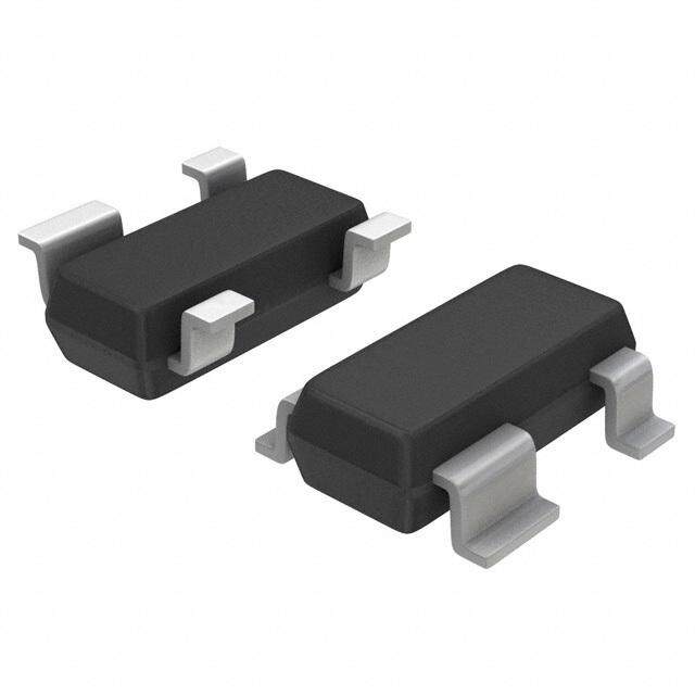
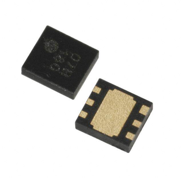
| 供应商器件封装 | TSOT-23-8 |
| 其它名称 | LTC2935ITS8-3#TRMPBFCT |
| 包装 | 剪切带 (CT) |
| 受监控电压数 | 1 |
| 复位 | 低有效 |
| 复位超时 | 最小为 140 ms |
| 安装类型 | 表面贴装 |
| 封装/外壳 | SOT-23-8 薄型,TSOT-23-8 |
| 工作温度 | -40°C ~ 85°C |
| 标准包装 | 1 |
| 电压-阈值 | 8 种可选阀值组合 |
| 类型 | 多压监控器 |
| 输出 | 开路漏极或开路集电极 |
| 配用 | /product-detail/zh/DC2042A/DC2042A-ND/4866639 |


PDF Datasheet 数据手册内容提取
LTC2935 Ultra-Low Power Supervisor with Power-Fail Output, Selectable Thresholds FEATURES DESCRIPTION n 500nA Quiescent Current The LTC®2935 ultra-low power voltage monitor provides n ±1.5% (Max) Accuracy over Temperature system initialization, power-fail warning and reset gen- n Integrated Precision Attenuators eration functions. Low quiescent current (500nA typical) n Eight Pin-Selectable Reset Thresholds makes the LTC2935 an ideal choice for battery-operated n Eight Pin-Selectable Power-Fail Thresholds applications. n Early Warning Power-Fail Output Three binary threshold-select inputs confi gure one of n 200ms Reset Timeout eight integrated reset thresholds, ranging from 1.6V to n Manual Reset Input 3.45V in pre-determined increments. Early warning of an n Compact 8-Lead, 2mm × 2mm DFN and impending low voltage condition is provided at the power- TSOT-23 (ThinSOT™) Packages fail output (PFO), whose threshold is above the confi gured reset threshold. Supervisory circuits monitor V and CC APPLICATIONS pull RST low when V drops below the confi gured reset CC threshold. When V is rising from an under-threshold CC n Portable Equipment condition, an internal reset timer is started after exceeding n Battery-Powered Equipment the reset threshold by 5%. A 200ms reset timeout delays n Security Systems the return of the RST output to a high state. A pushbut- n Point-of-Sale Devices ton switch connected to the MR input is typically used to n Wireless Systems force a manual reset. Outputs RST and PFO are available L, LT, LTC, LTM, Linear Technology and the Linear logo are registered trademarks of Linear with open-drain (LTC2935-1/LTC2935-3) or active pull-up Technology Corporation. ThinSOT is a trademark of Linear Technology Corporation. All other trademarks are the property of their respective owners. (LTC2935-2/LTC2935-4) circuits. Operating temperature range is from –40°C to 85°C. TYPICAL APPLICATION Falling Threshold Selection Table Confi gurable Low Power Voltage Monitor LTC2935-1/LTC2935-2 LTC2935-3/LTC2935-4 VIN RESET POWER-FAIL RESET POWER-FAIL THRESHOLD THRESHOLD THRESHOLD THRESHOLD VCC (V) (V) (V) (V) S2 S1 S0 S2 PFO 0.1μF 3.30 3.45 2.44 2.56 Low Low Low S1 BATTERY LTC2935-2 POWERED 3.15 3.30 2.32 2.44 Low Low High S0 SYSTEM LOGIC 3.00 3.15 2.20 2.32 Low High High MR RST 2.85 3.00 2.08 2.20 Low High Low GND 2.70 2.85 1.96 2.08 High High Low 2935 TA01a 2.55 2.70 1.84 1.96 High Low Low 2.40 2.55 1.72 1.84 High Low High 2.25 2.40 1.60 1.72 High High High 2935fa 1
LTC2935 ABSOLUTE MAXIMUM RATINGS (Notes 1, 2) Input Voltages Operating Ambient Temperature Range V ...........................................................–0.3V to 6V LTC2935C ................................................0°C to 70°C CC S2, S1, S0, MR .........................–0.3V to (V + 0.3V) LTC2935I..............................................–40°C to 85°C CC Output Voltages (PFO, RST) Storage Temperature Range ...................–65°C to 150°C LTC2935-1/LTC2935-3 .............................–0.3V to 6V Lead Temperature (Soldering, 10 sec) LTC2935-2/LTC2935-4 ..............–0.3V to (V + 0.3V) TSOT-23 Package ..............................................300°C CC RMS Currents PFO, RST ..........................................................±5mA PIN CONFIGURATION TOP VIEW TOP VIEW VCC 1 8 S2 MR 2 7 S1 S2 1 8VCC 9 S1 2 7MR RST 3 6 S0 S0 3 6RST PFO 4 5 GND GND 4 5PFO TS8 PACKAGE DC PACKAGE 8-LEAD PLASTIC TSOT-23 8-LEAD (2mm (cid:115) 2mm) PLASTIC DFN TJMAX = 125°C, θJA = 102°C/W TJMAX = 125°C, θJA = 195°C/W EXPOSED PAD (PIN 9), PCB GND CONNECTION OPTIONAL ORDER INFORMATION Lead Free Finish TAPE AND REEL (MINI) TAPE AND REEL PART MARKING* PACKAGE DESCRIPTION TEMPERATURE RANGE LTC2935CTS8-1#TRMPBF LTC2935CTS8-1#TRPBF LTDPW 8-Lead Plastic TSOT-23 0°C to 70°C LTC2935ITS8-1#TRMPBF LTC2935ITS8-1#TRPBF LTDPW 8-Lead Plastic TSOT-23 –40°C to 85°C LTC2935CTS8-2#TRMPBF LTC2935CTS8-2#TRPBF LTDQB 8-Lead Plastic TSOT-23 0°C to 70°C LTC2935ITS8-2#TRMPBF LTC2935ITS8-2#TRPBF LTDQB 8-Lead Plastic TSOT-23 –40°C to 85°C LTC2935CTS8-3#TRMPBF LTC2935CTS8-3#TRPBF LTFHV 8-Lead Plastic TSOT-23 0°C to 70°C LTC2935ITS8-3#TRMPBF LTC2935ITS8-3#TRPBF LTFHV 8-Lead Plastic TSOT-23 –40°C to 85°C LTC2935CTS8-4#TRMPBF LTC2935CTS8-4#TRPBF LTFHX 8-Lead Plastic TSOT-23 0°C to 70°C LTC2935ITS8-4#TRMPBF LTC2935ITS8-4#TRPBF LTFHX 8-Lead Plastic TSOT-23 –40°C to 85°C LTC2935CDC-1#TRMPBF LTC2935CDC-1#TRPBF LDPX 8-Lead (2mm × 2mm) Plastic DFN 0°C to 70°C LTC2935IDC-1#TRMPBF LTC2935IDC-1#TRPBF LDPX 8-Lead (2mm × 2mm) Plastic DFN –40°C to 85°C LTC2935CDC-2#TRMPBF LTC2935CDC-2#TRPBF LDQC 8-Lead (2mm × 2mm) Plastic DFN 0°C to 70°C LTC2935IDC-2#TRMPBF LTC2935IDC-2#TRPBF LDQC 8-Lead (2mm × 2mm) Plastic DFN –40°C to 85°C LTC2935CDC-3#TRMPBF LTC2935CDC-3#TRPBF LFHW 8-Lead (2mm × 2mm) Plastic DFN 0°C to 70°C LTC2935IDC-3#TRMPBF LTC2935IDC-3#TRPBF LFHW 8-Lead (2mm × 2mm) Plastic DFN –40°C to 85°C LTC2935CDC-4#TRMPBF LTC2935CDC-4#TRPBF LFHY 8-Lead (2mm × 2mm) Plastic DFN 0°C to 70°C LTC2935IDC-4#TRMPBF LTC2935IDC-4#TRPBF LFHY 8-Lead (2mm × 2mm) Plastic DFN –40°C to 85°C TRM = 500 pieces. *Temperature grades are identifi ed by a label on the shipping container. Consult LTC Marketing for parts specifi ed with wider operating temperature ranges. Consult LTC Marketing for information on lead based fi nish parts. For more information on lead free part marking, go to: http://www.linear.com/leadfree/ For more information on tape and reel specifi cations, go to: http://www.linear.com/tapeandreel/ 2935fa 2
LTC2935 ELECTRICAL CHARACTERISTICS The l denotes the specifi cations which apply over the full operating temperature range, otherwise specifi cations are at T = 25°C, V = 3.6V, unless otherwise noted. (Note 2) A CC SYMBOL PARAMETER CONDITIONS MIN TYP MAX UNITS V V Input Supply Voltage l 5.5 V CC CC I V Input Supply Current l 225 500 1000 nA CC CC Reset Thresholds (LTC2935-1/LTC2935-2) V Reset Threshold 1 (V Falling) S2 = Low : S1 = Low : S0 = Low l 3.251 3.300 3.349 V RTF1 CC V Reset Threshold 2 (V Falling) S2 = Low : S1 = Low : S0 = High l 3.103 3.150 3.197 V RTF2 CC V Reset Threshold 3 (V Falling) S2 = Low : S1 = High : S0 = High l 2.955 3.000 3.045 V RTF3 CC V Reset Threshold 4 (V Falling) S2 = Low : S1 = High : S0 = Low l 2.808 2.850 2.892 V RTF4 CC V Reset Threshold 5 (V Falling) S2 = High : S1 = High : S0 = Low l 2.660 2.700 2.740 V RTF5 CC V Reset Threshold 6 (V Falling) S2 = High : S1 = Low : S0 = Low l 2.512 2.550 2.588 V RTF6 CC V Reset Threshold 7 (V Falling) S2 = High : S1 = Low : S0 = High l 2.364 2.400 2.436 V RTF7 CC V Reset Threshold 8 (V Falling) S2 = High : S1 = High : S0 = High l 2.217 2.250 2.283 V RTF8 CC ΔVRTF Reset Threshold Differential VRTF(N+1) – VRTF(N) (Note 3) l 142 150 158 mV V Reset Threshold Hysteresis (V Rising) Relative to Any Selected Reset Threshold l 4.5 5 6 % RT(HYST) CC t Undervoltage Detect to RST Falling V Below Threshold by 1% (Note 3) 1 ms UVR CC Reset Thresholds (LTC2935-3/LTC2935-4) V Reset Threshold 1 (V Falling) S2 = Low : S1 = Low : S0 = Low l 2.404 2.440 2.476 V RTF1 CC V Reset Threshold 2 (V Falling) S2 = Low : S1 = Low : S0 = High l 2.286 2.320 2.354 V RTF2 CC V Reset Threshold 3 (V Falling) S2 = Low : S1 = High : S0 = High l 2.167 2.200 2.233 V RTF3 CC V Reset Threshold 4 (V Falling) S2 = Low : S1 = High : S0 = Low l 2.049 2.080 2.111 V RTF4 CC V Reset Threshold 5 (V Falling) S2 = High : S1 = High : S0 = Low l 1.931 1.960 1.989 V RTF5 CC V Reset Threshold 6 (V Falling) S2 = High : S1 = Low : S0 = Low l 1.813 1.840 1.867 V RTF6 CC V Reset Threshold 7 (V Falling) S2 = High : S1 = Low : S0 = High l 1.695 1.720 1.745 V RTF7 CC V Reset Threshold 8 (V Falling) S2 = High : S1 = High : S0 = High l 1.576 1.600 1.624 V RTF8 CC ΔVRTF Reset Threshold Differential VRTF(N+1) – VRTF(N) (Note 3) l 112 120 128 mV V Reset Threshold Hysteresis (V Rising) Relative to Any Selected Reset Threshold l 4.5 5 6 % RT(HYST) CC t Undervoltage Detect to RST Falling V Below Threshold by 1% (Note 3) 1 ms UVR CC Power-Fail Thresholds (LTC2935-1/LTC2935-2) ΔVPFT Power-Fail Threshold Differential VPFT(N) – VRTF(N) Any Selected Reset Threshold (VCC Falling) l 100 150 200 mV V Power-Fail Threshold Hysteresis Relative to Any Selected Power-Fail Threshold l 2 2.5 3.5 % PFT(HYST) (V Rising) CC t Undervoltage Detect to PFO Falling V Below Threshold by 1% (Note 3) 1 ms UVP CC Power-Fail Thresholds (LTC2935-3/LTC2935-4) ΔVPFT Power-Fail Threshold Differential VPFT(N) – VRTF(N) Any Selected Reset Threshold (VCC Falling) l 70 120 170 mV V Power-Fail Threshold Hysteresis Relative to Any Selected Power-Fail Threshold l 2 2.5 3 % PFT(HYST) (V Rising) CC t Undervoltage Detect to PFO Falling V Below Threshold by 1% (Note 3) 1 ms UVP CC Control Inputs: MR, S2, S1, S0 V Control Input Threshold S2, S1, S0 l 0.3 • V 0.7 • V V IN(TH) CC CC MR l 0.4 1.4 V t Input Pulse Width MR l 20 μs PW t Propagation Delay to RST Falling Manual Reset Falling l 2 5 20 μs PD R Internal Pull-Up Resistance MR l 600 900 1200 kΩ PU I Input Leakage Current S2, S1, S0 = V or GND l ±1 ±10 nA LK CC 2935fa 3
LTC2935 ELECTRICAL CHARACTERISTICS The l denotes the specifi cations which apply over the full operating temperature range, otherwise specifi cations are at T = 25°C, V = 3.6V, unless otherwise noted. (Note 2) A CC SYMBOL PARAMETER CONDITIONS MIN TYP MAX UNITS Reset and Power-Fail Outputs: RST, PFO V Voltage Output Low V = 1V, 200μA Pull-Up Current l 25 100 mV OL CC V = 3V, 3mA Pull-Up Current l 50 150 mV CC S2, S1, S0 = Low V Voltage Output High (LTC2935-2) –200μA Pull-Down Current l 0.7 • V V OH CC I Current Output High, Leakage (LTC2935-1) V , V = 3.6V l ±1 ±10 nA OH RST PFO t Reset Timeout Period l 140 200 260 ms RST Note 1: Stresses beyond those listed under Absolute Maximum Ratings Note 2. All currents into pins are positive, all voltages are referenced to may cause permanent damage to the device. Exposure to any Absolute GND unless otherwise noted. Maximum Rating condition for extended periods may affect device Note 3. Guaranteed by design. Characterized, but not production tested. reliability and lifetime. TYPICAL PERFORMANCE CHARACTERISTICS T = 25°C, unless otherwise noted. A Normalized Reset and Power-Fail Comparator Undervoltage Supply Current vs Supply Voltage Thresholds vs Temperature Glitch Immunity 1000 1.015 3.0 S0 = S1 = S2 = GND VCC = 3.6V 800 85°C V/V) 1.010 s) 2.5 OLD ( 1.005 (mUV 2.0 (nA)C600 25°C THRESH 1.000 ATION, t 1.5 CAOBOMVPEA RCUATROVRES PULL DOWN IC400 –40°C LIZED 0.995 H DUR 1.0 A C M T R LI 200 NO 0.990 G 0.5 0 0.985 0 0 1 2 3 4 5 6 –50 –25 0 25 50 75 100 0.1 1 10 100 VCC (V) TEMPERATURE (°C) COMPARATOR OVERDRIVE (%) 2935 G01 2935 G02 2935 G03 Reset Timeout Period Voltage Output Low vs Pull-Up Voltage Output High vs Pull-Down vs Temperature Current (RST, PFO) Current (RST, PFO) 260 100 3.6 VCC= 3.6V VCC= 3V LTC2935-2 85°C VCC= 3.6V 240 80 3.5 220 25°C t (ms)RST200 V (mV)OL 4600 –40°C V (mV)OH 3.4 –2450°°CC 180 3.3 160 20 85°C 140 0 3.2 –50 –25 0 25 50 75 100 0 1 2 3 4 5 0 –0.2 –0.4 –0.6 –0.8 –1 TEMPERATURE (°C) PULL-UP CURRENT (mA) PULL-DOWN CURRENT (mA) 2935 G04 2935 G05 2935 G06 2935fa 4
LTC2935 TYPICAL PERFORMANCE CHARACTERISTICS T = 25°C, unless otherwise noted. A Supply Current vs S0, S1, S2 Input Voltage Supply Current vs MR Input Voltage 250 5 VCC = 3.6V VCC = 3.6V 200 4 150 3 A) A) μ μ (C (C C C I 100 I 2 50 1 0 0 0 0.5 1 1.5 2 2.5 3 3.5 4 0 0.5 1 1.5 2 2.5 3 3.5 4 S0, S1, S2 INPUT VOLTAGE (V) MR INPUT VOLTAGE (V) 2935 G07 2935 G08 PIN FUNCTIONS Exposed Pad (DFN Only): Exposed Pad may be left fl oating RST: Reset Output. RST pulls low when V falls below the CC or connected to device ground. reset threshold. RST is released 200ms after V exceeds CC the reset threshold plus 5% hysteresis. RST is available GND: Device ground. with open-drain (LTC2935-1/LTC2935-3) or active pull-up MR: Manual Reset Input. Attach a pushbutton switch (LTC2935-2/LTC2935-4) outputs. Leave open if unused. between this input and ground. A logic low on this input S2, S1, S0: Threshold Selection Inputs. Tie to GND or pulls RST low. When the MR input returns to logic high, V for required reset threshold. See the Falling Threshold RST returns high after 200ms. Tie to V if unused. CC CC Selection Table on page 1 for settings. PFO: Power-Fail Output. PFO pulls low when V falls CC V : Power Supply and Monitored Voltage Input. Bypass below the power-fail threshold. The power-fail thresh- CC V with a 0.1μF capacitor to GND. old is above the confi gured falling reset threshold by a CC pre-determined margin. PFO is released when V rises CC above the power-fail threshold by 2.5%. PFO is available with open-drain (LTC2935-1/LTC2935-3) or active pull-up (LTC2935-2/LTC2935-4) outputs. Leave open if unused. 2935fa 5
LTC2935 BLOCK DIAGRAM MR LTC2935-2/LTC2935-4 VCC VCC 900k RST RC – RESET DELAY S0 + LTC2935-2/LTC2935-4 S1 VCC S2 0.4V PC PFO + – GND 2935 BD TIMING DIAGRAM VPFT VRTF VCC PFO tRST tRST RST MR 2935 TD tPD 2935fa 6
LTC2935 APPLICATIONS INFORMATION VOLTAGE MONITORING or replacement. An internal reset timer delays the return of the RST output to a high state to provide settling and Unmanaged power can cause various system problems. initialization time. The RST output is typically connected At power-up, voltage fl uctuation around critical thresholds to a processor reset input. can cause improper system or processor initialization. The LTC2935 provides power management capabilities Few, if any external components are necessary for reliable for the system power-up phase. The supervisory device operation. However, a decoupling capacitor between V CC issues a system reset after the monitored voltage has and ground is recommended (0.01μF minimum). stabilized. Built-in hysteresis and fi ltering ensures that fl uctuations due to load transients or supply noise do Threshold Confi guration not cause chattering of the status outputs. Comparator The LTC2935 monitors and compares the V voltage CC undervoltage glitch immunity is shown in the Typical against two internal thresholds during operation. The Performance Characteristics section. The curve dem- higher threshold (power-fail) is the level used for early onstrates the transient amplitude and width required to warning of a low voltage condition, reported on the PFO switch the comparators. output. The lower threshold (reset) is the level at which the Because many batteries exhibit large series resistance, RST output pulls low. Use system requirements to choose load currents can cause signifi cant voltage drops. The the appropriate reset threshold from Table 1. low DC current draw of the LTC2935 (at any input volt- Table 1. Falling Threshold Selection age) does not add to the loading problem. When voltage LTC2935-1/LTC2935-2 LTC2935-3/LTC2935-4 is initially applied to V , RST and PFO pull low once there CC RESET POWER-FAIL RESET POWER-FAIL is enough voltage to turn on the pull-down devices (1V THRESHOLD THRESHOLD THRESHOLD THRESHOLD maximum). (V) (V) (V) (V) S2 S1 S0 3.30 3.45 2.44 2.56 Low Low Low If the monitored supply voltage falls to the power-fail 3.15 3.30 2.32 2.44 Low Low High threshold, the built-in power-fail comparator pulls PFO 3.00 3.15 2.20 2.32 Low High High low. At this point, there remains a voltage margin before 2.85 3.00 2.08 2.20 Low High Low the RST output pulls low. PFO remains low until V rises CC 2.70 2.85 1.96 2.08 High High Low above the power-fail threshold plus 2.5% hysteresis. PFO is typically used in signal preparation for controlled shut- 2.55 2.70 1.84 1.96 High Low Low down. For example, the PFO output may be connected to 2.40 2.55 1.72 1.84 High Low High a processor nonmaskable interrupt. Upon interrupt, the 2.25 2.40 1.60 1.72 High High High processor may begin shutdown procedures. Shutdown In the LTC2935-1/LTC2935-2 the power-fail threshold events may include supply sequencing and/or storage/ is always 150mV higher than the confi gured reset erasure of system state in nonvolatile memory. threshold. In the LTC2935-3/LTC2935-4 the power-fail threshold is always 120mV higher than the confi gured If the monitored voltage drops below the reset threshold, reset threshold. Set the threshold selection inputs (S2, RST pulls low until V rises above the reset threshold plus CC S1, S0) accordingly. 5% hysteresis. This may occur through battery charging 2935fa 7
LTC2935 APPLICATIONS INFORMATION Selecting Output Logic Style undetermined voltages when connected to high impedance (such as CMOS logic inputs). The resistor value should The LTC2935 status outputs are available in two op- be small enough to provide effective pull-down without tions: open-drain (LTC2935-1/LTC2935-3) or active excessively loading the pull-up circuitry. A 100k resistor pull-up (LTC2935-2/LTC2935-4). The open-drain options from output to ground is satisfactory for most applications. (LTC2935-1/LTC2935-3) allow the outputs to be pulled up When the status outputs are high, power is dissipated in to a user defi ned voltage with a resistor. The open-drain pull-up voltage may be greater than V (5.5V maximum), the pull-down resistors. Figure 2 demonstrates typical CC which is not always possible with inferior battery supervi- LTC2935-2/LTC2935-4 RST output behavior. sors, due to internal clamps. When the status outputs are Manual Reset Input low, power is dissipated in the pull-up resistors. Recom- mended resistor values lie in the range between 10k and When V is above its reset threshold, and the manual CC 470k. Figure 1 demonstrates typical LTC2935-1/LTC2935-3 reset input (MR) is pulled low, the RST output is forced low. RST output behavior. RST remains low for 200ms after the manual reset input is The active pull-up options (LTC2935-2/LTC2935-4) elimi- released and pulled high. The manual reset input is pulled nate the need for external pull-up resistors on the status up internally through 900k to VCC. If external leakage cur- outputs. Integrated pull-up devices pull the outputs up to rents have the ability to pull down the manual reset input V . Actively pulled up outputs may not be driven above below its logic threshold, a lower value pull-up resistor, CC V . placed between V and MR will fi x the problem. CC CC Some applications require the RST and/or PFO outputs to Input MR is often pulled down through a pushbutton be valid with V down to ground. Active pull-up handles switch requiring human contact. If extended ESD toler- CC this requirement with the addition of an external resistor ance is required, series resistance between the switch and from the output to ground. The resistor provides a path the input is recommended. For most applications, a 10k for leakage currents, preventing the output from fl oating to resistor provides suffi cient current limiting. 3.5 3.5 LTC2935-1 LTC2935-2 S2 = GND S2 = GND 3.0 S1 = S0 = VCC 3.0 S1 = S0 = VCC 2.5 2.5 V) 2.0 V) 2.0 T ( T ( S S R 1.5 R 1.5 1.0 1.0 0.5 0.5 0 0 0 0.5 1 1.5 2 2.5 3 3.5 0 0.5 1 1.5 2 2.5 3 3.5 VCC (V) 2935 F01 VCC (V) 2935 F02 Figure 1. RST vs V with 10k Pull-Up Figure 2. RST vs V CC CC 2935fa 8
LTC2935 TYPICAL APPLICATIONS Battery Monitor with Interface to Low Voltage Logic 3μA LDO 1.8V IN LT3009 OUT SHDN GND ADJ 1.18M 1μF 590k 100k 100k VCC VDD + S0 PFO NMI Li-Ion 0.1μF S1 LTC2935-1 S2 μP RESD* 10k MR RST RST MANUAL GND RESET PB1 PUSHBUTTON POWER FAIL FALLING THRESHOLD = 3.15V 2935 TA02 RESET FALLING THRESHOLD = 3.00V *OPTIONAL RESISTOR FOR ADDED ESD PROTECTION Alkaline Cell Stack Voltage Monitor VCC MR + S0 PFO LOW BATTERY 1.5V 0.1μF S2 LTC2935-2 + S1 1.5V RST SYSTEM RESET + 1.5V GND 2935 TA03 POWER FAIL FAIL THRESHOLD = 2.55V RESET THRESHOLD = 2.40V Coin Cell Voltage Monitor VCC MR + S2 PFO LOW BATTERY CR2032 0.1μF S1 LTC2935-2 S0 RST SYSTEM RESET GND 2935 TA04 POWER FAIL FAIL THRESHOLD = 2.70V RESET THRESHOLD = 2.55V 2935fa 9
LTC2935 PACKAGE DESCRIPTION DC Package 8-Lead Plastic DFN (2mm × 2mm) (Reference LTC DWG # 05-08-1719 Rev Ø) 0.70 ±0.05 2.55 ±0.05 1.15 ±0.050.64 ±0.05 (2 SIDES) PACKAGE OUTLINE 0.25 ± 0.05 0.45 BSC 1.37 ±0.05 (2 SIDES) RECOMMENDED SOLDER PAD PITCH AND DIMENSIONS APPLY SOLDER MASK TO AREAS THAT ARE NOT SOLDERED R = 0.115 TYP R = 0.05 5 8 TYP 0.40 ± 0.10 2.00 ±0.10 0.64 ± 0.10 PIN 1 NOTCH PIN 1 BAR (4 SIDES) (2 SIDES) R = 0.20 OR TOP MARK 0.25 × 45° (SEE NOTE 6) CHAMFER (DC8) DFN 0106 REVØ 4 1 0.23 ± 0.05 0.200 REF 0.75 ±0.05 0.45 BSC 1.37 ±0.10 (2 SIDES) 0.00 – 0.05 BOTTOM VIEW—EXPOSED PAD NOTE: 1. DRAWING IS NOT A JEDEC PACKAGE OUTLINE 2. DRAWING NOT TO SCALE 3. ALL DIMENSIONS ARE IN MILLIMETERS 4. DIMENSIONS OF EXPOSED PAD ON BOTTOM OF PACKAGE DO NOT INCLUDE MOLD FLASH. MOLD FLASH, IF PRESENT, SHALL NOT EXCEED 0.15mm ON ANY SIDE 5. EXPOSED PAD SHALL BE SOLDER PLATED 6. SHADED AREA IS ONLY A REFERENCE FOR PIN 1 LOCATION ON THE TOP AND BOTTOM OF PACKAGE 2935fa 10
LTC2935 PACKAGE DESCRIPTION TS8 Package 8-Lead Plastic TSOT-23 (Reference LTC DWG # 05-08-1637) 2.90 BSC 0.52 0.65 (NOTE 4) MAX REF 1.22 REF 1.50 – 1.75 3.85 MAX2.62 REF 1.4 MIN 2.80 BSC (NOTE 4) PIN ONE ID RECOMMENDED SOLDER PAD LAYOUT 0.22 – 0.36 0.65 BSC PER IPC CALCULATOR 8 PLCS (NOTE 3) 0.80 – 0.90 0.20 BSC 0.01 – 0.10 1.00 MAX DATUM ‘A’ 0.30 – 0.50 REF 1.95 BSC 0.09 – 0.20 (NOTE 3) TS8 TSOT-23 0802 NOTE: 1. DIMENSIONS ARE IN MILLIMETERS 2. DRAWING NOT TO SCALE 3. DIMENSIONS ARE INCLUSIVE OF PLATING 4. DIMENSIONS ARE EXCLUSIVE OF MOLD FLASH AND METAL BURR 5. MOLD FLASH SHALL NOT EXCEED 0.254mm 6. JEDEC PACKAGE REFERENCE IS MO-193 2935fa Information furnished by Linear Technology Corporation is believed to be accurate and reliable. 11 However, no responsibility is assumed for its use. Linear Technology Corporation makes no representa- tion that the interconnection of its circuits as described herein will not infringe on existing patent rights.
LTC2935 TYPICAL APPLICATION Portable Device Battery Monitor 3μA LDO 1.8V IN LT3009 OUT VCC MR 100k SHDN GND ADJ 1.18M + S0 Li-Ion 0.1μF 1μF S1 RST LTC2935-1 100k S2 590k LOW BATTERY PFO GND EARLY WARNING POWER FAIL FALLING THRESHOLD = 3.15V 2935 TA05 RESET FALLING THRESHOLD = 3.00V RELATED PARTS PART NUMBER DESCRIPTION COMMENTS LTC690 5V Supply Monitor, Watchdog Timer and Battery Backup 4.65V Threshold LTC694-3.3 3.3V Supply Monitor, Watchdog Timer and Battery Backup 2.9V Threshold LTC1232 5V Supply Monitor, Watchdog Timer and Pushbutton Reset 4.37V/4.62V Threshold LTC1326 Micropower Triple Supply Monitor for 5V/2.5V, 3.3V and ADJ 4.725V, 3.118V, 1V Threshold (±0.75%) and ADJ LTC1726 Micropower Triple Supply Monitor for 2.5V/5V, 3.3V and ADJ Adjustable Reset and Watchdog Timeouts LTC1727 Micropower Triple Supply Monitor with Open-Drain Reset Individual Monitor Outputs in MSOP LTC1728 Micropower Triple Supply Monitor with Open-Drain Reset 5-Lead SOT-23 Package LTC1985 Micropower Triple Supply Monitor with Push-Pull Reset Output 5-Lead SOT-23 Package LTC2900 Programmable Quad Supply Monitor Adjustable Reset, 10-Lead MSOP and DFN Packages LTC2901 Programmable Quad Supply Monitor Adjustable Reset and Watchdog Timer LTC2902 Programmable Quad Supply Monitor Adjustable Reset and Tolerance LTC2903 Precision Quad Supply Monitor 6-Lead SOT-23 Package LTC2904/LTC2905/ Three-State Programmable Precision Dual Supply Monitor 8-Lead SOT-23 and DFN Packages LTC2906/LTC2907 LTC2908 Precision Six-Supply Monitor (Four Fixed and Two Adjustable) 8-Lead TSOT-23 and DFN Packages LTC2909 Precision Triple/Dual Input UV, OV and Negative Voltage Monitor Shunt Regulated V Pin, Adjustable Threshold and Reset, CC 8-Lead SOT-23 and DFN Packages LTC2910 Octal Positive/Negative Voltage Monitor Separate V Pin, Eight Inputs, Up to Two Negative Monitors CC Adjustable Reset Timer, 16-Lead SSOP and DFN Packages LTC2912/LTC2913/ Single/Dual/Quad UV and OV Voltage Monitors Separate V Pin, Adjustable Reset Timer CC LTC2914 LTC2915/LTC2916/ Single Voltage Supervisors with 27 Pin-Selectable Thresholds Manual Reset and Watchdog Functions LTC2917/LTC2918 LTC2934 Ultralow Power Supervisor with Power-Fail Output 500nA Quiescent Current, 2mm × 2mm 8-Lead DFN and TSOT-23 Packages, Adjustable via External Resistors 2935fa 12 Linear Technology Corporation LT 0609 REV A • PRINTED IN USA 1630 McCarthy Blvd., Milpitas, CA 95035-7417 (408) 432-1900 ● FAX: (408) 434-0507 ● www.linear.com © LINEAR TECHNOLOGY CORPORATION 2008