ICGOO在线商城 > 集成电路(IC) > PMIC - 监控器 > XC61CN2502MR-G
 Datasheet下载
- 型号: XC61CN2502MR-G
- 制造商: TOREX SEMICONDUCTOR
- 库位|库存: xxxx|xxxx
- 要求:
| 数量阶梯 | 香港交货 | 国内含税 |
| +xxxx | $xxxx | ¥xxxx |
查看当月历史价格
查看今年历史价格
XC61CN2502MR-G产品简介:
ICGOO电子元器件商城为您提供XC61CN2502MR-G由TOREX SEMICONDUCTOR设计生产,在icgoo商城现货销售,并且可以通过原厂、代理商等渠道进行代购。 XC61CN2502MR-G价格参考¥2.25-¥6.22。TOREX SEMICONDUCTORXC61CN2502MR-G封装/规格:PMIC - 监控器, 开路漏极或开路集电极 监控器 1 通道 SOT-23。您可以下载XC61CN2502MR-G参考资料、Datasheet数据手册功能说明书,资料中有XC61CN2502MR-G 详细功能的应用电路图电压和使用方法及教程。
Torex Semiconductor Ltd的XC61CN2502MR-G是一款电源管理集成电路(PMIC)中的电压监控器,主要用于监测系统中的电源电压是否在正常范围内。该芯片具有高精度电压检测功能,适用于对电源稳定性要求较高的电子设备。

其主要应用场景包括:

1. 嵌入式系统与工业控制:用于监控系统主电源或备用电源的电压状态,确保控制系统稳定运行,防止因电压异常导致的数据丢失或硬件损坏。

2. 消费类电子产品:如智能家电、数码相机、便携式音频设备等,用于实时监控电池或适配器供电电压,保障设备安全工作。

3. 通信设备:在路由器、交换机等网络设备中,用于监测供电电压,及时发出复位信号以防止系统异常。

4. 汽车电子系统:如车载导航、行车记录仪等,用于监控车辆电源系统的电压变化,确保设备在复杂电气环境中可靠运行。

5. 医疗仪器:用于精密仪器的电源监控,确保设备在电压异常时能及时响应,保护患者和设备安全。

该器件采用小型封装,功耗低,适合空间受限且需要高稳定性的应用场合。
| 参数 | 数值 |
| 产品目录 | 集成电路 (IC) |
| 描述 | IC SUPERVISOR 2.5V SOT23-3 |
| 产品分类 | |
| 品牌 | Torex Semiconductor Ltd |
| 数据手册 | |
| 产品图片 |
|
| 产品型号 | XC61CN2502MR-G |
| rohs | 无铅 / 符合限制有害物质指令(RoHS)规范要求 |
| 产品系列 | - |
| 产品目录页面 | |
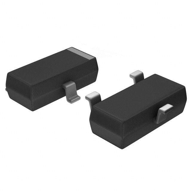
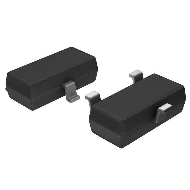
| 供应商器件封装 | SOT-23 |
| 其它名称 | 893-1033-6 |
| 包装 | Digi-Reel® |
| 受监控电压数 | 1 |
| 复位 | - |
| 复位超时 | - |
| 安装类型 | 表面贴装 |
| 封装/外壳 | TO-236-3,SC-59,SOT-23-3 |
| 工作温度 | -40°C ~ 85°C |
| 标准包装 | 1 |
| 电压-阈值 | 2.5V |
| 类型 | 简单复位/加电复位 |
| 输出 | 开路漏极或开路集电极 |


- 商务部:美国ITC正式对集成电路等产品启动337调查
- 曝三星4nm工艺存在良率问题 高通将骁龙8 Gen1或转产台积电
- 太阳诱电将投资9.5亿元在常州建新厂生产MLCC 预计2023年完工
- 英特尔发布欧洲新工厂建设计划 深化IDM 2.0 战略
- 台积电先进制程称霸业界 有大客户加持明年业绩稳了
- 达到5530亿美元!SIA预计今年全球半导体销售额将创下新高
- 英特尔拟将自动驾驶子公司Mobileye上市 估值或超500亿美元
- 三星加码芯片和SET,合并消费电子和移动部门,撤换高东真等 CEO
- 三星电子宣布重大人事变动 还合并消费电子和移动部门
- 海关总署:前11个月进口集成电路产品价值2.52万亿元 增长14.8%


PDF Datasheet 数据手册内容提取
XC61C Series ETR0201_016 Low Voltage Detectors (V = 0.8V~1.5V) DF Standard Voltage Detectors (V 1.6V~6.0V) DF ■GENERAL DESCRIPTION The XC61C series are highly precise, low power consumption voltage detectors, manufactured using CMOS and laser trimming technologies. Detect voltage is extremely accurate with minimal temperature drift. Both CMOS and N-ch open drain output configurations are available. ■APPLICATIONS ■FEATURES ●Microprocessor reset circuitry Highly Accurate : ± 2% : ± 1%(Standard Voltage VD: 2.6V~5.1V) ●Memory battery back-up circuits Low Power Consumption : 0.7μA (TYP.) [VIN=1.5V] ●Power-on reset circuits Detect Voltage Range : 0.8V ~ 6.0V in 0.1V increments Operating Voltage Range : 0.7V ~ 6.0V (Low Voltage) ●Power failure detection 0.7V~10.0V (Standard Voltage) ●System battery life and charge voltage monitors Detect Voltage Temperature Characteristics : ±100ppm/℃ (TYP.) Output Configuration : N-ch open drain or CMOS Packages : SSOT-24 SOT-23 SOT-89 Environmentally Friendly : EU RoHS Compliant, Pb Free ■TYPICAL APPLICATION CIRCUITS ■TYPICAL PERFORMANCE CHARACTERISTICS 1/16
XC61C Series ■PIN CONFIGURATION ■PIN ASSIGNMENT PIN NUMBER PIN NAME FUNCTIONS SSOT-24 SOT-23 SOT-89 2 3 2 VIN Supply Voltage Input 4 2 3 VSS Ground 1 1 1 VOUT Output 3 - - NC No Connection ■PRODUCT CLASSIFICATION ●Ordering Information XC61C①②③④⑤⑥⑦-⑧(*1) DESIGNATOR ITEM SYMBOL DESCRIPTION C CMOS output ① Output Configuration N N-ch open drain output e.g.0.9V → ②0, ③9 ②③ Detect Voltage 08 ~ 60 e.g.1.5V → ②1, ③5 ④ Output Delay 0 No delay ⑤ Detect Accuracy 1 Within ±1% (VDF(T)=2.6V~5.1V) 2 Within ±2% NR SSOT-24 (3,000pcs/Reel) NR-G SSOT-24 (3,000pcs/Reel) MR SOT-23 (3,000pcs/Reel) ⑥⑦-⑧ (*1) Packages (Order Unit) MR-G SOT-23 (3,000pcs/Reel) PR SOT-89 (1,000pcs/Reel) PR-G SOT-89 (1,000pcs/Reel) (*1) The “-G” suffix denotes Halogen and Antimony free as well as being fully EU RoHS compliant. 2/16
XC61C Series ■BLOCK DIAGRAMS (1) CMOS Output (2) N-ch Open Drain Output ■ABSOLUTE MAXIMUM RATINGS Ta = 25OC PARAMETER SYMBOL RATINGS UNITS *1 VSS-0.3 ~ 9.0 Input Voltage VIN V *2 VSS-0.3 ~ 12.0 Output Current IOUT 50 mA CMOS VSS -0.3 ~ VIN +0.3 Output Voltage N-ch Open Drain Output *1 VOUT VSS -0.3 ~ 9.0 V N-ch Open Drain Output *2 VSS -0.3 ~ 12.0 SSOT-24 150 Power Dissipation SOT-23 Pd 150 mW SOT-89 500 Operating Ambient Temperature Topr -40~+85 ℃ Storage Temperature Tstg -55~+125 ℃ *1: Low voltage: VDF(T)=0.8V~1.5V *2: Standard voltage: VDF(T)=1.6V~6.0V 3/16
XC61C Series ■ELECTRICAL CHARACTERISTICS VDF (T) = 0.8V to 6.0V ± 2% VDF (T) = 2.6V to 5.1V ± 1% Ta=25℃ PARAMETER SYMBOL CONDITIONS MIN. TYP. MAX. UNITS CIRCUITS VDF(T)=0.8V~1.5V *1 VDF(T) VDF(T) VDF(T) V 1 VDF(T)=1.6V~6.0V *2 x 0.98 x 1.02 Detect Voltage VDF VDF(T) VDF(T) VDF(T)=2.6V~5.1V *2 VDF(T) V 1 x 0.99 x 1.01 VDF VDF VDF Hysteresis Range VHYS V 1 x 0.02 x 0.05 x 0.08 VIN = 1.5V - 0.7 2.3 VIN = 2.0V - 0.8 2.7 Supply Current ISS VIN = 3.0V - 0.9 3.0 μA 2 VIN = 4.0V - 1.0 3.2 VIN = 5.0V - 1.1 3.6 Operating Voltage *1 VDF(T) = 0.8V to 1.5V 0.7 - 6.0 VIN V 1 Operating Voltage *2 VDF(T) = 1.6V to 6.0V 0.7 - 10.0 VIN = 0.7V 0.10 0.80 - N-ch VDS = 0.5V 3 Output Current *1 VIN = 1.0V 0.85 2.70 - CMOS, P-ch VDS = 2.1V VIN = 6.0V - -7.5 -1.5 4 VIN = 1.0V 1.0 2.2 - IOUT VIN = 2.0V 3.0 7.7 - mA N-ch VDS = 0.5V VIN = 3.0V 5.0 10.1 - 3 Output Current *2 VIN = 4.0V 6.0 11.5 - VIN = 5.0V 7.0 13.0 - CMOS, P-ch VDS = 2.1V VIN = 8.0V - -10.0 -2.0 4 CMOS Output VIN=VDFx0.9, VOUT=0V - -10 - Leakage (Pch) ILEAK nA 3 Current N-ch VIN=6.0V, VOUT=6.0V*1 Open - 10 100 VIN=10.0V, VOUT=10.0V*2 Drain Temperature ΔVDF/ -40℃ ≦ Topr ≦ 85℃ - ±100 - ppm/ 1 Characteristics (ΔTopr・VDF) ℃ Delay Time (VDR→VOUT inversion) tDLY Inverts from VDR to VOUT - 0.03 0.20 ms 5 NOTE: *1: Low Voltage: VDF(T)=0.8V~1.5V *2: Standard Voltage: VDF(T)=1.6V~6.0V VDF (T): Nominal detect voltage Release Voltage: VDR = VDF + VHYS 4/16
XC61C Series ■OPERATIONAL EXPLANATION (Especially prepared for CMOS output products) ① When input voltage (VIN) is higher than detect voltage (VDF), output voltage (VOUT) will be equal to VIN. (A condition of high impedance exists with N-ch open drain output configurations.) ② When input voltage (VIN) falls below detect voltage (VDF), output voltage (VOUT) will be equal to the ground voltage (VSS) level. ③ When input voltage (VIN) falls to a level below that of the minimum operating voltage (VMIN), output will become unstable. (As for the N-ch open drain product of XC61CN, the pull-up voltage goes out at the output voltage.) ④ When input voltage (VIN) rises above the ground voltage (VSS) level, output will be unstable at levels below the minimum operating voltage (VMIN). Between the VMIN and detect release voltage (VDR) levels, the ground voltage (VSS) level will be maintained. ⑤ When input voltage (VIN) rises above detect release voltage (VDR), output voltage (VOUT) will be equal to VIN. (A condition of high impedance exists with N-ch open drain output configurations.) ⑥ The difference between VDR and VDF represents the hysteresis range. ●Timing Chart 5/16
XC61C Series ■NOTES ON USE 1. Please use this IC within the stated absolute maximum ratings. For temporary, transitional voltage drop or voltage rising phenomenon, the IC is liable to malfunction should the ratings be exceeded. 2. When a resistor is connected between the VIN pin and the power supply with CMOS output configurations, oscillation may occur as a result of voltage drops at RIN if load current (IOUT) exists. (refer to the Oscillation Description (1) below) 3. When a resistor is connected between the VIN pin and the power supply with CMOS output configurations, irrespective of N-ch open-drain output configurations, oscillation may occur as a result of through current at the time of voltage release even if load current (IOUT) does not exist. (refer to the Oscillation Description (2) below ) 4. Please use N-ch open drain output configuration, when a resistor RIN is connected between the VIN pin and power source. In such cases, please ensure that RIN is less than 10kΩ and that C is more than 0.1μF, please test with the actual device. (refer to the Oscillation Description (1) below) 5. With a resistor RIN connected between the VIN pin and the power supply, the VIN pin voltage will be getting lower than the power supply voltage as a result of the IC's supply current flowing through the VIN pin. 6. In order to stabilize the IC's operations, please ensure that VIN pin input frequency's rise and fall times are more than 2 μ s/ V. 7. Torex places an importance on improving our products and its reliability. However, by any possibility, we would request user fail-safe design and post-aging treatment on system or equipment. Power supply ●Oscillation Description (1) Load current oscillation with the CMOS output configuration When the voltage applied at power supply, release operations commence and the detector's output voltage increases. Load current (IOUT) will flow at RL. Because a voltage drop (RIN x IOUT) is produced at the RIN resistor, located between the power supply and the VIN pin, the load current will flow via the IC's VIN pin. The voltage drop will also lead to a fall in the voltage level at the VIN pin. When the VIN pin voltage level falls below the detect voltage level, detect operations will commence. Following detect operations, load current flow will cease and since voltage drop at RIN will disappear, the voltage level at the VIN pin will rise and release operations will begin over again. Oscillation may occur with this " release - detect - release " repetition. Further, this condition will also appear via means of a similar mechanism during detect operations. (2) Oscillation as a result of through current Since the XC61C series are CMOS IC S, through current will flow when the IC's internal circuit switching operates (during release and detect operations). Consequently, oscillation is liable to occur as a result of drops in voltage at the through current's resistor (RIN) during release voltage operations. (refer to Figure 3) Since hysteresis exists during detect operations, oscillation is unlikely to occur. Power supply Power supply 6/16
XC61C Series 100kΩ* 7/16
XC61C Series ■TYPICAL PERFORMANCE CHARACTERISTICS ●Low Voltage Note : Unless otherwise stated, the N-ch open drain pull-up resistance value is 100kΩ. 8/16
XC61C Series ■TYPICAL PERFORMANCE CHARACTERISTICS (Continued) ●Low Voltage (Continued) (4) N-ch Driver Output Current vs. VDS XC61CC0902(0.9V) XC61CC1102(1.1V) XC61CC1102(1.1V) 1.4 1.4 3.0 Ta=25℃ Ta=25℃ Ta=25℃ mA) 1.2 VIN =0.8V mA) 1.2 VIN =0.8V mA) 2.5 VIN=1.0V (UT 1.0 (UT 1.0 (UT 2.0 nt: IO 0.8 nt: IO 0.8 nt: IO 1.5 ut Curre 00..46 0.7V ut Curre 00..46 0.7V ut Curre 1.0 utp 0.2 utp 0.2 utp 0.5 O O O 0 0 0 0 0.2 0.4 0.6 0.8 1.0 0 0.2 0.4 0.6 0.8 1.0 0 0.2 0.4 0.6 0.8 1.0 VDS(V) VDS(V) VDS(V) XC61CC1502(1.5V) XC61CC1502(1.5V) 1.4 8.0 Ta=25℃ Ta=25℃ mA) 1.2 VIN =0.8V mA) 6.0 VIN=1.4V (UT 1.0 (UT O O nt: I 0.8 nt: I 4.0 1.2V urre 0.6 0.7V urre C C ut 0.4 ut 2.0 1.0V p p ut 0.2 ut O O 0 0 0 0.2 0.4 0.6 0.8 1.0 0 0.2 0.4 0.6 0.8 1.0 1.2 1.4 VDS(V) VDS(V) (5) N-ch Driver Output Current vs. InputVoltage XC61CC0902(0.9V) XC61CC1102(1.1V) XC61CC1502(1.5V) 2.5 5.0 10 VDS=0.5V VDS=0.5V Ta=-40℃ VDS=0.5V mA) 2.0 mA) 4.0 mA) 8 Ta=-40℃ (UT (UT 25℃ (UT 25℃ nt: IO 1.5 nt: IO 3.0 nt: IO 6 e e e put Curr 01..50 25T℃a=85℃ put Curr 12..00 80℃ put Curr 24 85℃ Out -40℃ Out Out 0 0 0 0 0.2 0.4 0.6 0.8 1.0 0 0.2 0.4 0.6 0.8 1.0 1.2 0 0.2 0.4 0.6 0.8 1.0 1.2 1.4 1.6 InputVoltage:VIN(V) InputVoltage: VIN (V) InputVoltage: VIN (V) (6) P-ch Driver Output Current vs. InputVoltage XC61CC0902(0.9V) XC61CC1102 (1.1V) XC61CC1502(1.5V) 12 12 12 Ta=25℃ VDS=2.1V Ta=25℃ VDS=2.1V Ta=25℃ VDS=2.1V A) 10 A) 10 A) 10 m m m Current: I (OUT 468 110...505VVV Current: I (OUT 468 110...505VVV Current: I (OUT 468 110...505VVV Output 2 Output 2 Output 2 0 0 0 0 1 2 3 4 5 6 0 1 2 3 4 5 6 0 1 2 3 4 5 6 InputVoltage:VIN(V) InputVoltage:VIN(V) InputVoltage:VIN(V) 9/16
XC61C Series ■TYPICAL PERFORMANCE CHARACTERISTICS (Continued) ●Standard Voltage (1) Supply Current vs. InputVoltage XC61CC1802(1.8V) XC61CC2702(2.7V) 3.5 3.5 3.0 3.0 A) A) μ μ 2.5 2.5 (S (S nt: IS 2.0 25℃ Ta=85℃ nt: IS 2.0 25℃ Ta=85℃ urre 1.5 urre 1.5 y C 1.0 y C 1.0 ppl 0.5 -40℃ ppl 0.5 -40℃ u u S S 0 0 0 2 4 6 8 10 0 2 4 6 8 10 InputVoltage: VIN (V) InputVoltage: VIN (V) XC61CC3602(3.6V) XC61CC4502(4.5V) 3.5 3.5 3.0 3.0 A) A) μ 2.5 μ 2.5 nt: I (SS 2.0 25℃ Ta=85℃ (nt: ISS 2.0 25℃ Ta=85℃ e 1.5 e 1.5 urr urr y C 1.0 y C 1.0 ppl 0.5 -40℃ ppl 0.5 -40℃ u u S S 0 0 0 2 4 6 8 10 0 2 4 6 8 10 InputVoltage: VIN (V) InputVoltage: VIN (V) (2) Detect, ReleaseVoltage vs. AmbientTemperature XC61CC1802 (1.8V) XC61CC2702(2.7V) 1.90 2.80 V) V) V(DR V(DR VDR V,DF 1.85 VDR V,DF 2.75 Voltage: Voltage: Release 1.80 VDF Release 2.70 VDF Detect, 1.75 Detect, 2.65 -50 -25 0 25 50 75 100 -50 -25 0 25 50 75 100 AmbientTemperature:Ta(℃) AmbientTemperature:Ta(℃) XC61CC3602(3.6V) XC61CC4502(4.5V) 3.8 4.7 V) V) (R (R VDR VD VDR VD V,DF 3.7 V,DF 4.6 ge: ge: a a olt olt V V e e as 3.6 as 4.5 e e Rel VDF Rel VDF ect, ect, et et D 3.5 D 4.4 -50 -25 0 25 50 75 100 -50 -25 0 25 50 75 100 AmbientTemperature:Ta(℃) AmbientTemperature:Ta(℃) 10/16
XC61C Series ■TYPICAL PERFORMANCE CHARACTERISTICS (Continued) ●Standard Voltage (Continued) (3) OutputVoltage vs. InputVoltage XC61CN1802(1.8V) XC61CN2702(2.7V) 2 3 Ta=25℃ Ta=25℃ V) V) (OUT (OUT 2 V V ge: 1 ge: a a Volt Volt 1 put put ut ut O O 0 0 0 1 2 0 1 2 3 InputVoltage: VIN (V) InputVoltage: VIN (V) XC61CN3602(3.6V) XC61CN4502(4.5V) 4 5 Ta=25℃ Ta=25℃ V) V) 4 (T 3 (T U U O O V V 3 ge: 2 ge: a a olt olt 2 V V ut 1 ut p p 1 ut ut O O 0 0 0 1 2 3 4 0 1 2 3 4 5 InputVoltage: VIN (V) InputVoltage: VIN (V) NNoottee :: TThhee NN--cchha onpneenl odpraeinn dprualiln u ppu rlel suips traensciset avnacluee v iasl u1e0 0isk Ω10.0 k Ω. (4) N-ch Driver Output Current vs. VDS XC61CC1802 (1.8V) XC61CC2702(2.7V) 10 30 Ta=25℃ VIN =1.5V Ta=25℃ A) 8 A) 25 VIN =2.5V m m (UT (UT 20 O 6 O 2.0V nt: I nt: I 15 e e utput Curr 24 1.0V utput Curr 150 1.5V O O 1.0V 0 0 0 0.5 1.0 1.5 2.0 0 0.5 1.0 1.5 2.0 2.5 3.0 VDS(V) VDS (V) XC61CC4502 (4.5V) XC61CC3602(3.6V) XC61XCC6C1C4C5450022 ((44.5V.5品V)) 80 40 80 Ta=25℃ Ta=25℃ 70 Ta=25℃ VIN=4.0V A) VIN =3.0V A) 70 m 30 m 6600 (T (T VIN =4.0V 33.5.5VV ent: IOU 20 2.5V ent: IOU 45450000 3.03V.0V Curr 2.0V Curr 3300 2.52.V5V put 10 put 2200 2.20.V0V Out 1.5V Out 1100 1.15.5VV 0 00 0 0.5 1.0 1.5 2.0 2.5 3.0 0 0.5 1.0 1.5 2.0 2.5 3.0 3.5 4.0 0 0.5 1.0 1.5 2.0 2.5 3.0 3.5 4.0 VDS(V) VDVSDS(V (V)) 11/16
XC61C Series ■TYPICAL PERFORMANCE CHARACTERISTICS (Continued) ●Standard Voltage (Continued) (4) N-ch Driver Output Current vs. VDS XC61CC1802(1.8V) XC61CC2702(2.7V) 1000 1000 Ta=25℃ VIN=0.8V Ta=25℃ A) A) μ 800 μ 800 (T (T VIN =0.8V U U O 600 O 600 nt: I 0.7V nt: I e e Curr 400 Curr 400 0.7V put 200 put 200 ut ut O O 0 0 0 0.2 0.4 0.6 0.8 1.0 0 0.2 0.4 0.6 0.8 1.0 VDS(V) VDS (V) XC61CC3602(3.6V) XC61CC4502(4.5V) 1000 1000 Ta=25℃ Ta=25℃ A) A) μ 800 VIN =0.8V μ 800 VIN=0.8V (T (T U U O 600 O 600 nt: I nt: I e e urr 400 0.7V urr 400 0.7V C C put 200 put 200 ut ut O O 0 0 0 0.2 0.4 0.6 0.8 1.0 0 0.2 0.4 0.6 0.8 1.0 VDS(V) VDS (V) (5) N-ch Driver Output Current vs. InputVoltage XC61CC1802(1.8V) XC61CC2702(2.7V) 15 25 VDS=0.5V VDS=0.5V Ta=-40℃ mA) Ta=-40℃ mA) 20 (OUT 10 25℃ (OUT 15 25℃ nt: I nt: I e e Curr 5 Curr 10 85℃ put 85℃ put 5 ut ut O O 0 0 0 0.5 1.0 1.5 2.0 0 0.5 1.0 1.5 2.0 2.5 3.0 InputVoltage: VIN (V) InputVoltage:VIN(V) XC61CC3602(3.6V) XC61CC4502(4.5V) 30 40 A) 25 VDS=0.5V Ta=-40℃ A) VDS=0.5V Ta=-40℃ m m 30 (UT 20 25℃ (UT 25℃ O O I I nt: 15 nt: 20 e e Curr 10 85℃ Curr 85℃ ut ut 10 utp 5 utp O O 0 0 0 1 2 3 4 0 1 2 3 4 5 InputVoltage:VIN(V) InputVoltage:VIN(V) 12/16
XC61C Series ■TYPICAL PERFORMANCE CHARACTERISTICS (Continued) ●Standard Voltage (Continued) (6) P-ch Driver Output Current vs. InputVoltage XC61CC1802(1.8V) XC61CC2702(2.7V) 15 15 VDS=2.1V VDS=2.1V A) A) m 1.5V m 1.5V (T 10 (T 10 U U IO IO ent: 1.0V ent: 1.0V Curr 5 Curr 5 put 0.5V put 0.5V ut ut O O 0 0 0 2 4 6 8 10 0 2 4 6 8 10 InputVoltage:VIN(V) InputVoltage:VIN(V) XC61CC3602(3.6V) XC61CC4502(4.5V) 15 15 VDS=2.1V VDS=2.1V A) A) m m 1.5V (UT 10 1.5V (UT 10 O O nt: I 1.0V nt: I 1.0V e e urr urr ut C 5 0.5V ut C 5 0.5V utp utp O O 0 0 0 2 4 6 8 10 0 2 4 6 8 10 InputVoltage: VIN (V) InputVoltage: VIN (V) 13/16
XC61C Series ■PACKAGING INFORMATION ●SSOT-24 ●SOT-23 2.0±0.1 +0.15 +0.15 0.25-0.1 0.25-0.1 +0.1 0-0 +0.1 +0.15 +0.15 0.125-0.05 0.25-0.1 0.35-0.1 0.05 1.3±0.2 ●SOT-89 ) 4 . (0 2.5±0.1 4.0±0.25 2 . 0 ± .0 1 ) 1 0. ( 1 ±0. .4) 5 0 . ( 1 5) 8 1. ( ) 5 .2 0 ( 14/16
XC61C Series ■MARKING RULE ● SSOT-24, SOT-23, SOT-89 ① represents integer of detect voltage and CMOS Output (XC61CC series) 4 3 MARK CONFIGURATION VOLTAGE (V) A CMOS 0.X ① ② ④ B CMOS 1.X C CMOS 2.X 1 2 D CMOS 3.X E CMOS 4.X F CMOS 5.X H CMOS 6.X 3 N-Channel Open Drain Output (XC61CN series) ① ② ③ ④ MARK CONFIGURATION VOLTAGE (V) K N-ch 0.X 1 2 L N-ch 1.X M N-ch 2.X N N-ch 3.X P N-ch 4.X R N-ch 5.X S N-ch 6.X ② ④ ② represents decimal number of detect voltage ① ③ MARK VOLTAGE (V) MARK VOLTAGE (V) 0 X.0 5 X.5 1 2 3 1 X.1 6 X.6 2 X.2 7 X.7 3 X.3 8 X.8 4 X.4 9 X.9 ③ represents delay time (Except for SSOT-24) MARK DELAY TIME PRODUCT SERIES 3 No Delay Time XC61Cxxx0xxx ④ represents production lot number Based on the internal standard. (G, I, J, O, Q, W excluded) 15/16
XC61C Series 1. The product and product specifications contained herein are subject to change without notice to improve performance characteristics. Consult us, or our representatives before use, to confirm that the information in this datasheet is up to date. 2. The information in this datasheet is intended to illustrate the operation and characteristics of our products. We neither make warranties or representations with respect to the accuracy or completeness of the information contained in this datasheet nor grant any license to any intellectual property rights of ours or any third party concerning with the information in this datasheet. 3. Applicable export control laws and regulations should be complied and the procedures required by such laws and regulations should also be followed, when the product or any information contained in this datasheet is exported. 4. The product is neither intended nor warranted for use in equipment of systems which require extremely high levels of quality and/or reliability and/or a malfunction or failure which may cause loss of human life, bodily injury, serious property damage including but not limited to devices or equipment used in 1) nuclear facilities, 2) aerospace industry, 3) medical facilities, 4) automobile industry and other transportation industry and 5) safety devices and safety equipment to control combustions and explosions. Do not use the product for the above use unless agreed by us in writing in advance. 5. Although we make continuous efforts to improve the quality and reliability of our products; nevertheless Semiconductors are likely to fail with a certain probability. So in order to prevent personal injury and/or property damage resulting from such failure, customers are required to incorporate adequate safety measures in their designs, such as system fail safes, redundancy and fire prevention features. 6. Our products are not designed to be Radiation-resistant. 7. Please use the product listed in this datasheet within the specified ranges. 8. We assume no responsibility for damage or loss due to abnormal use. 9. All rights reserved. No part of this datasheet may be copied or reproduced unless agreed by Torex Semiconductor Ltd in writing in advance. TOREX SEMICONDUCTOR LTD. 16/16