ICGOO在线商城 > 射频/IF 和 RFID > RFID,RF 接入,监控 IC > RF430CL330HCPWR
 Datasheet下载
- 型号: RF430CL330HCPWR
- 制造商: Texas Instruments
- 库位|库存: xxxx|xxxx
- 要求:
| 数量阶梯 | 香港交货 | 国内含税 |
| +xxxx | $xxxx | ¥xxxx |
查看当月历史价格
查看今年历史价格
RF430CL330HCPWR产品简介:
ICGOO电子元器件商城为您提供RF430CL330HCPWR由Texas Instruments设计生产,在icgoo商城现货销售,并且可以通过原厂、代理商等渠道进行代购。 RF430CL330HCPWR价格参考¥2.92-¥2.97。Texas InstrumentsRF430CL330HCPWR封装/规格:RFID,RF 接入,监控 IC, RFID Transponder IC 13.56MHz ISO 14443, NFC I²C, SPI 2 V ~ 3.6 V 14-TSSOP (0.173", 4.40mm Width)。您可以下载RF430CL330HCPWR参考资料、Datasheet数据手册功能说明书,资料中有RF430CL330HCPWR 详细功能的应用电路图电压和使用方法及教程。
Texas Instruments 的 RF430CL330HCPWR 是一款集成 RFID 和传感功能的监控 IC,属于高频(13.56MHz)RFID 标签芯片。其主要应用场景包括:

1. 智能医疗监护:可用于贴附在医疗器械或患者身上的无线传感器节点,实现体温、心率等生理参数的非接触式读取与传输。

2. 冷链物流监控:嵌入在冷链运输标签中,实时监测并记录温度变化,保障药品、食品等对温敏要求高的物品运输安全。

3. 资产追踪与管理:用于高价值设备或工具的智能化标识,结合 NFC 手机或读写器实现快速识别和状态查询。

4. 智能包装与防伪溯源:应用于高端商品包装中,通过内置传感器检测是否开封或环境异常,增强产品防伪与质量控制能力。

5. 工业环境监测:用于监测关键设备的温度、湿度等参数,支持预测性维护,提升工业自动化水平。

该芯片集成了低功耗 MCU、EEPROM、传感器接口和 ISO/IEC 15693/NFC-V 协议,无需外部电源即可工作,适用于无源、便携式的智能传感系统。
| 参数 | 数值 |
| 产品目录 | |
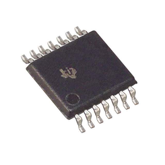
| 描述 | IC NFC DYNAMIC TAG TARG 14-TSSOPRFID应答器 NFC Type-4 Compliant Tag |
| 产品分类 | |
| 品牌 | Texas Instruments |
| 产品手册 | http://www.ti.com/lit/gpn/rf430cl330h |
| 产品图片 |
|
| rohs | 符合RoHS无铅 / 符合限制有害物质指令(RoHS)规范要求 |
| 产品系列 | RF集成电路,RFID应答器,Texas Instruments RF430CL330HCPWR- |
| 数据手册 | |
| 产品型号 | RF430CL330HCPWR |
| RF类型 | 读/写 |
| 产品培训模块 | http://www.digikey.cn/PTM/IndividualPTM.page?site=cn&lang=zhs&ptm=30374 |
| 产品种类 | RFID应答器 |
| 供应商器件封装 | 14-TSSOP |
| 其它名称 | 296-36223-1 |
| 功能 | NFC connection handover for an alternative carrier like Bluetooth |
| 包装 | 剪切带 (CT) |
| 商标 | Texas Instruments |
| 安装风格 | SMD/SMT |
| 封装 | Reel |
| 封装/外壳 | 14-TSSOP(0.173",4.40mm 宽) |
| 封装/箱体 | TSSOP-14 |
| 工作温度范围 | 0 C to + 70 C |
| 工厂包装数量 | 2000 |
| 最大工作温度 | + 70 C |
| 最小工作温度 | 0 C |
| 标准包装 | 1 |
| 特性 | ISO14443-B |
| 系列 | RF430CL330H |
| 频率 | 13.56MHz |


- 商务部:美国ITC正式对集成电路等产品启动337调查
- 曝三星4nm工艺存在良率问题 高通将骁龙8 Gen1或转产台积电
- 太阳诱电将投资9.5亿元在常州建新厂生产MLCC 预计2023年完工
- 英特尔发布欧洲新工厂建设计划 深化IDM 2.0 战略
- 台积电先进制程称霸业界 有大客户加持明年业绩稳了
- 达到5530亿美元!SIA预计今年全球半导体销售额将创下新高
- 英特尔拟将自动驾驶子公司Mobileye上市 估值或超500亿美元
- 三星加码芯片和SET,合并消费电子和移动部门,撤换高东真等 CEO
- 三星电子宣布重大人事变动 还合并消费电子和移动部门
- 海关总署:前11个月进口集成电路产品价值2.52万亿元 增长14.8%


PDF Datasheet 数据手册内容提取
Product Sample & Technical Tools & Support & Reference Folder Buy Documents Software Community Design RF430CL330H SLAS916C–NOVEMBER2012–REVISEDNOVEMBER2014 RF430CL330H Dynamic NFC Interface Transponder 1 Device Overview 1.1 Features 1 • NFCTagType4 • 3KBofSRAMforNDEFMessages • ISO14443B-Compliant13.56-MHzRFInterface • AutomaticCheckingofNDEFStructure Supportsupto848kbps • InterruptRegisterandOutputPintoIndicateNDEF • SPIorI2CInterfacetoWriteandReadNDEF ReadorWriteCompletion MessagestoInternalSRAM 1.2 Applications • Bluetooth®Pairing • DiagnosticInterface • Wi-Fi®Configuration • SensorInterface 1.3 Description TheTexasInstrumentsDynamicNFCInterfaceTransponderRF430CL330HisanNFCTagType4device that combines a wireless NFC interface and a wired SPI or I2C interface to connect the device to a host. The NDEF message in the SRAM can be written and read from the integrated SPI or I2C serial communication interface and can also be accessed and updated wirelessly through the integrated ISO14443B-compliantRFinterfacethatsupportsupto848kbps. This operation allows NFC connection handover for an alternative carrier like Bluetooth, Bluetooth Low Energy(BLE),andWi-Fiasaneasyandintuitivepairingprocessorauthenticationprocesswithonlyatap. As a general NFC interface, the RF430CL330H enables end equipments to communicate with the fast- growinginfrastructureofNFC-enabledsmartphones,tablets,andnotebooks. Table1-1.DeviceInformation(1) PARTNUMBER PACKAGE BODYSIZE(2) RF430CL330HPW TSSOP(14) 5mmx4.4mm RF430CL330HRGT VQFN(16) 3mmx3mm (1) Forthemostcurrentpart,package,andorderinginformationforallavailabledevices,seethePackage OptionAddenduminSection7,orseetheTIwebsiteatwww.ti.com. (2) Thesizesshownhereareapproximations.Forthepackagedimensionswithtolerances,seethe MechanicalDatainSection7. 1.4 Typical Application Diagram Figure1-1showsatypicalapplicationdiagramforthe RF430CL330Hdevice. I2C or SPI RF430 NFC Micro- NFC controller Tag Reader INTO Figure1-1.TypicalApplication 1 AnIMPORTANTNOTICEattheendofthisdatasheetaddressesavailability,warranty,changes,useinsafety-criticalapplications, intellectualpropertymattersandotherimportantdisclaimers.PRODUCTIONDATA.
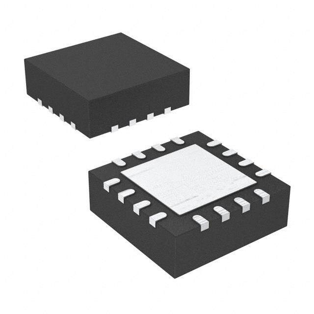
RF430CL330H SLAS916C–NOVEMBER2012–REVISEDNOVEMBER2014 www.ti.com Table of Contents 1 DeviceOverview......................................... 1 4.15 RF143B,PowerSupply............................. 11 1.1 Features.............................................. 1 5 DetailedDescription................................... 12 ........................................... ........................... 1.2 Applications 1 5.1 FunctionalBlockDiagram 12 ............................................ ..................... 1.3 Description 1 5.2 SerialCommunicationInterface 12 1.4 TypicalApplicationDiagram.......................... 1 5.3 SPIorI2CModeSelection.......................... 12 2 Revision History......................................... 2 5.4 CommunicationProtocol............................ 13 3 TerminalConfigurationandFunctions.............. 3 5.5 I2CProtocol ......................................... 14 4 Specifications ............................................ 6 5.6 SPIProtocol......................................... 17 .......................... ............................................ 4.1 AbsoluteMaximumRatings 6 5.7 Registers 23 ..................................... ...................... 4.2 Handling Ratings 6 5.8 NFCType-4TagFunctionality 29 ................ ...................................... 4.3 RecommendedOperatingConditions 6 5.9 NDEFMemory 33 4.4 RecommendedOperatingConditions,Resonant 5.10 TypicalUsageScenario............................. 36 ................................................. Circuit 6 .......................................... 5.11 References 36 ...................................... 4.5 Supply Currents 7 6 DeviceandDocumentationSupport............... 37 .......................................... 4.6 Digital Inputs 7 ...................................... 6.1 DeviceSupport 37 ........................................ 4.7 Digital Outputs 7 ............................. 6.2 DocumentationSupport 38 .............................. 4.8 Thermal Characteristics 8 .............................. 6.3 CommunityResources 38 ............. 4.9 SerialCommunicationProtocolTimings 9 .......................................... 6.4 Trademarks 39 4.10 I2C Interface.......................................... 9 ..................... 6.5 ElectrostaticDischargeCaution 39 ........................................ 4.11 SPIInterface 10 ............................................. 6.6 Glossary 39 .... 4.12 RF143B,RecommendedOperatingConditions 11 7 MechanicalPackagingandOrderable 4.13 RF143B,ISO14443BASKDemodulator............ 11 Information.............................................. 39 4.14 RF143B,ISO14443B-CompliantLoadModulator... 11 7.1 PackagingInformation .............................. 39 2 Revision History NOTE:Pagenumbersforpreviousrevisionsmaydifferfrompagenumbersinthecurrentversion. ChangesfromRevisionB(June2014)toRevisionC Page • AddedRGTpackagetoDeviceInformationtable................................................................................ 1 • AddedRGTpackagepinout......................................................................................................... 3 • AddedRGTpackagetoTable3-1.................................................................................................. 4 • AddedSection4.8.................................................................................................................... 8 2 RevisionHistory Copyright©2012–2014,TexasInstrumentsIncorporated SubmitDocumentationFeedback ProductFolderLinks:RF430CL330H
RF430CL330H www.ti.com SLAS916C–NOVEMBER2012–REVISEDNOVEMBER2014 3 Terminal Configuration and Functions Figure3-1showsthepinassignmentsforthePWpackage. VCC 1 14 VSS ANT1 2 13 VCORE ANT2 3 12 SI/SDA RST 4 11 SO/SCL E0 5 10 SCK E1 6 9 SCMS/CS E2 7 8 INTO Figure3-1.14-PinPWPackage(TopView) Figure3-2showsthepinassignmentsfortheRGTpackage. C S C C C S N V N V 16 15 14 13 ANT1 1 12 VCORE ANT2 2 Exposed 11 SI/SDA Thermal RST 3 10 SO/SCL Pad E0 4 9 SCK 5 6 7 8 1 2 O S E E T C N S/ I M C S Figure3-2.16-PinRGTPackage(TopView) Copyright©2012–2014,TexasInstrumentsIncorporated TerminalConfigurationandFunctions 3 SubmitDocumentationFeedback ProductFolderLinks:RF430CL330H
RF430CL330H SLAS916C–NOVEMBER2012–REVISEDNOVEMBER2014 www.ti.com Table3-1.TerminalFunctions TERMINAL NO. I/O DESCRIPTION NAME PW RGT VCC 1 15 PWR 3.3-Vpowersupply ANT1 2 1 RF Antennainput1 ANT2 3 2 RF Antennainput2 RST 4 3 I Resetinput(activelow) I2Caddressselect0 E0(TMS) 5 4 I SPImodeselect0 (JTAGtestmodeselect) I2Caddressselect1 E1(TDO) 6 5 I(O) SPImodeselect1 (JTAGtestdataoutput) I2Caddressselect2 E2(TDI) 7 6 I (JTAGtestdatain) Interruptoutput INTO(TCK) 8 7 O (JTAGtestclock) SCMS/ SerialCommunicationModeSelect(duringdeviceinitialization) 9 8 I CS Chipselect(inSPImode) SCK 10 9 I SPIclockinput(SPImode) SPIslaveout(SPImode) SO/SCL 11 10 I/O I2Cclock(I2Cmode) SPIslavein(SPImode) SI/SDA 12 11 I/O I2Cdata(I2Cmode) VCORE 13 12 PWR Regulatedcoresupplyvoltage VSS 14 13 PWR Groundsupply NC - 14,16 Leaveopen,Noconnection 4 TerminalConfigurationandFunctions Copyright©2012–2014,TexasInstrumentsIncorporated SubmitDocumentationFeedback ProductFolderLinks:RF430CL330H
RF430CL330H www.ti.com SLAS916C–NOVEMBER2012–REVISEDNOVEMBER2014 VCC C 1 C 2 VCC VSS 1 14 C Antenna C ANT1 VCORE Core Tune 2 13 ANT2 SI/SDA 3 12 SDA External Reset (optional) RST 4 11 SO/SCL SCL I2CAddress Select E0 SCK n/a for I2C 5 10 I2CAddress Select E1 SCMS/CS select I2C 6 9 I2CAddress Select E2 INTO Interrupt Output 7 8 NOTE: Forrecommendedcapacitancevalues,seeRecommendedOperatingConditions. Figure3-3.ExampleApplicationDiagram(I2COperation)(PWPackageShown) VCC C 1 C 2 VCC VSS 1 14 C Antenna C ANT1 VCORE Core Tune 2 13 ANT2 SI/SDA 3 12 SI External Reset (optional) RST 4 11 SO/SCL SO SPI Mode Select E0 SCK 5 10 SCK SPI Mode Select E1 SCMS/CS 6 9 CS n/a for SPI E2 INTO Interrupt Output 7 8 NOTE: Forrecommendedcapacitancevalues,seeRecommendedOperatingConditions. Figure3-4.ExampleApplicationDiagram(SPIOperation)(PWPackageShown) Copyright©2012–2014,TexasInstrumentsIncorporated TerminalConfigurationandFunctions 5 SubmitDocumentationFeedback ProductFolderLinks:RF430CL330H
RF430CL330H SLAS916C–NOVEMBER2012–REVISEDNOVEMBER2014 www.ti.com 4 Specifications 4.1 Absolute Maximum Ratings(1) (2) MIN MAX UNIT VoltageappliedatV referencedtoV (V ) -0.3 4.1 V CC SS AMR VoltageappliedatV referencedtoV (V ) -0.3 4.1 V ANT SS AMR Voltageappliedtoanypin(referencestoV ) -0.3 V +0.3 V SS CC Diodecurrentatanydevicepin ±2 mA (1) StressesbeyondthoselistedunderAbsoluteMaximumRatingsmaycausepermanentdamagetothedevice.Thesearestressratings only,andfunctionaloperationofthedeviceattheseoranyotherconditionsbeyondthoseindicatedunderRecommendedOperating Conditionsisnotimplied.Exposuretoabsolute-maximum-ratedconditionsforextendedperiodsmayaffectdevicereliability. (2) AllvoltagesarereferencedtoVSS. 4.2 Handling Ratings MIN MAX UNIT T Storagetemperaturerange(1) -40 125 °C stg (1) Forsolderingduringboardmanufacturing,itisrequiredtofollowthecurrentJEDECJ-STD-020specificationwithpeakreflow temperaturesnothigherthanclassifiedonthedevicelabelontheshippingboxesorreels. 4.3 Recommended Operating Conditions TypicalvaluesarespecifiedatV =3.3VandT =25°C(unlessotherwisenoted) CC A MIN NOM MAX UNIT SupplyvoltageduringprogramexecutionnoRFfieldpresent 3.0 3.3 3.6 V V CC SupplyvoltageduringprogramexecutionwithRFfieldpresent 2.0 3.3 3.6 V V Supplyvoltage(GNDreference) 0 V SS T Operatingfree-airtemperature -40 85 °C A C DecouplingcapacitoronV (1) 0.1 µF 1 CC C DecouplingcapacitoronV (1) 1 µF 2 CC C CapacitoronV (1) 0.1 0.47 1 µF VCORE CORE (1) Lowequivalentseriesresistance(ESR)capacitor 4.4 Recommended Operating Conditions, Resonant Circuit MIN NOM MAX UNIT f Carrierfrequency 13.56 MHz c V Antennainputvoltage 3.6 V ANT_peak Z ImpedanceofLCcircuit 6.5 15.5 kΩ L Coilinductance(1) 2.66 µH RES C Totalresonancecapacitance(1)C =C +C 51.8 pF RES RES IN Tune C – CTune Externalresonancecapacitance CRES(2) pF IN QT Tankqualityfactor 30 (1) ThecoilinductanceoftheantennaL togetherwiththeexternalcapacitanceC plusthedeviceinternalcapacitanceC isa RES Tune IN resonantcircuit.TheresonantfrequencyofthisLCcircuitmustbeclosetothecarrierfrequencyf : c f =1/[2π(L C )1/2]=1/[2π(L (C +C ))1/2]≈f RES RES RES RES IN Tune c (2) ForC refertoSection4.12. IN 6 Specifications Copyright©2012–2014,TexasInstrumentsIncorporated SubmitDocumentationFeedback ProductFolderLinks:RF430CL330H
RF430CL330H www.ti.com SLAS916C–NOVEMBER2012–REVISEDNOVEMBER2014 4.5 Supply Currents overrecommendedrangesofsupplyvoltageandoperatingfree-airtemperature(unlessotherwisenoted) PARAMETER TESTCONDITIONS V MIN TYP MAX UNIT CC SPI,f ,SO=Open, I SCK,MAX 3.3V 250 µA CC(SPI) WritingintoNDEFmemory I2C,400kHz,WritingintoNDEF I 3.3V 250 µA CC(I2C) memory I RFenabled,noRFfieldpresent 3.3V 40 µA CC(RFenabled) Standbyenable=0,RFdisabled, I 3.3V 15 µA CC(Inactive) noserialcommunication Standbyenable=1,RFdisabled, I 3.3V 10 45 µA CC(Standby) noserialcommunication Additionalcurrentconsumption ΔI 3.0Vto3.6V 160 µA CC(StrongRF) withstrongRFfieldpresent CurrentdrawnfromVCC<3.0V I withRFfieldpresent(passive 2.0Vto3.0V 0 µA CC(RF,lowVCC) operation) 4.6 Digital Inputs overrecommendedrangesofsupplyvoltageandoperatingfree-airtemperature(unlessotherwisenoted) PARAMETER TESTCONDITIONS V MIN TYP MAX UNIT CC 0.3× V Low-levelinputvoltage V IL V CC 0.7× V High-levelinputvoltage V IH V CC 0.1× V Inputhysteresis V HYS V CC I High-impedanceleakagecurrent 3.3V -50 50 nA L R IntegratedRSTpullupresistor 20 35 50 kΩ PU(RST) IntegratedSCMS/CSpullupresistor(onlyactiveduring R 20 35 50 kΩ PU(CS) initialization) 4.7 Digital Outputs overrecommendedrangesofsupplyvoltageandoperatingfree-airtemperature(unlessotherwisenoted) PARAMETER TESTCONDITIONS V MIN TYP MAX UNIT CC 3V 0.4 V Outputlowvoltage I =3mA 3.3V 0.4 V OL OL 3.6V 0.4 3V 2.6 V Outputhighvoltage I =-3mA 3.3V 2.9 V OH OH 3.6V 3.2 Copyright©2012–2014,TexasInstrumentsIncorporated Specifications 7 SubmitDocumentationFeedback ProductFolderLinks:RF430CL330H
RF430CL330H SLAS916C–NOVEMBER2012–REVISEDNOVEMBER2014 www.ti.com 4.8 Thermal Characteristics overoperatingfree-airtemperaturerange(unlessotherwisenoted) PARAMETER VALUE UNIT θ Junction-to-ambientthermalresistance,stillair(1) 116.0 °C/W JA θ Junction-to-case(top)thermalresistance(2) 45.1 °C/W JC(TOP) θ Junction-to-boardthermalresistance(3) TSSOP-14(PW) 57.6 °C/W JB Ψ Junction-to-boardthermalcharacterizationparameter 57.0 °C/W JB Ψ Junction-to-topthermalcharacterizationparameter 4.6 °C/W JT θ Junction-to-ambientthermalresistance,stillair(1) 48.8 °C/W JA θ Junction-to-case(top)thermalresistance(2) 60.8 °C/W JC(TOP) θ Junction-to-boardthermalresistance(3) 21.9 °C/W JB VQFN-16(RGT) Ψ Junction-to-boardthermalcharacterizationparameter 21.9 °C/W JB Ψ Junction-to-topthermalcharacterizationparameter 1.5 °C/W JT θ Junction-to-case(bottom)thermalresistance(4) 7.1 °C/W JC(BOT) (1) Thejunction-to-ambientthermalresistanceundernaturalconvectionisobtainedinasimulationonaJEDEC-standard,High-Kboard,as specifiedinJESD51-7,inanenvironmentdescribedinJESD51-2a. (2) Thejunction-to-case(top)thermalresistanceisobtainedbysimulatingacoldplatetestonthepackagetop.NospecificJEDEC standardtestexists,butaclosedescriptioncanbefoundintheANSISEMIstandardG30-88. (3) Thejunction-to-boardthermalresistanceisobtainedbysimulatinginanenvironmentwitharingcoldplatefixturetocontrolthePCB temperature,asdescribedinJESD51-8. (4) Thejunction-to-case(bottom)thermalresistanceisobtainedbysimulatingacoldplatetestontheexposed(power)pad.Nospecific JEDECstandardtestexists,butaclosedescriptioncanbefoundintheANSISEMIstandardG30-88. 8 Specifications Copyright©2012–2014,TexasInstrumentsIncorporated SubmitDocumentationFeedback ProductFolderLinks:RF430CL330H
RF430CL330H www.ti.com SLAS916C–NOVEMBER2012–REVISEDNOVEMBER2014 4.9 Serial Communication Protocol Timings overrecommendedrangesofsupplyvoltageandoperatingfree-airtemperature(unlessotherwisenoted) PARAMETER MIN TYP MAX UNIT t Timeafterpower-uporresetuntilSCMS/CSissampledforSPIorI2Cdecision(1) 1 10 ms SPIvsI2C t Timeafterpower-uporresetuntildeviceisreadytocommunicateusingSPIorI2C(2) 20 ms Ready (1) TheSCMS/CSpinissampledaftert (MIN)attheearliestandaftert (MAX)atthelatest. SPIvsI2C SPIvsI2C (2) Thedeviceisreadytocommunicateaftert (MAX)atthelatest. Ready 4.10 I2C Interface overrecommendedrangesofsupplyvoltageandoperatingfree-airtemperature(unlessotherwisenoted)(seeFigure4-1) TEST PARAMETER V MIN TYP MAX UNIT CONDITIONS CC SCLclockfrequency(withMastersupportingclock stretchingaccordingtoI2Cstandard,orwhenthedeviceis 3.3V 0 400 kHz notbeingaddressed) f SCL SCLclockfrequency(devicebeingaddressedbyMaster write 3.3V 0 120 kHz notsupportingclockstretching) read 3.3V 0 100 kHz f ≤100kHz 4 SCL t Holdtime(repeated)START 3.3V µs HD,STA f >100kHz 0.6 SCL f ≤100kHz 4.7 SCL t SetuptimeforarepeatedSTART 3.3V µs SU,STA f >100kHz 0.6 SCL t Dataholdtime 3.3V 0 ns HD,DAT t Datasetuptime 3.3V 250 ns SU,DAT t SetuptimeforSTOP 3.3V 4 µs SU,STO t Pulsedurationofspikessuppressedbyinputfilter 3.3V 6.25 75 ns SP t t t HD,STA SU,STA HD,STA SDA 1/f t SCL SP SCL t t SU,DAT SU,STO t HD,DAT Figure4-1.I2CModeTiming Copyright©2012–2014,TexasInstrumentsIncorporated Specifications 9 SubmitDocumentationFeedback ProductFolderLinks:RF430CL330H
RF430CL330H SLAS916C–NOVEMBER2012–REVISEDNOVEMBER2014 www.ti.com 4.11 SPI Interface overrecommendedrangesofsupplyvoltageandoperatingfree-airtemperature(unlessotherwisenoted) PARAMETER TESTCONDITIONS V MIN TYP MAX UNIT CC write 3.3V 0 100 kHz f SCKclockfrequency SCK read 3.3V 0 110 kHz t CShightime 3.3V 50 µs HIGH,CS t CSsetuptime 3.3V 25 µs SU,CS t CSholdtime 3.3V 100 ns HD,CS t SCKhightime 3.3V 100 ns HIGH t SCKlowtime 3.3V 100 ns LOW t DataIn(SI)setuptime 3.3V 50 ns SU,SI t DataIn(SI)holdtime 3.3V 50 ns HD,SI t Output(SO)valid 3.3V 0 50 ns VALID,SO t Output(SO)holdtime 3.3V 0 ns HOLD,SO t t t SU,CS HD,CS CS,HIGH CS 1/f SCK Mode 0 SCK Mode 3 t t t SU,SI LOW HIGH t HD,SI SI t VALID,SO SO Figure4-2.SPIModeTiming 10 Specifications Copyright©2012–2014,TexasInstrumentsIncorporated SubmitDocumentationFeedback ProductFolderLinks:RF430CL330H
RF430CL330H www.ti.com SLAS916C–NOVEMBER2012–REVISEDNOVEMBER2014 4.12 RF143B, Recommended Operating Conditions overrecommendedrangesofsupplyvoltageandoperatingfree-airtemperature(unlessotherwisenoted) PARAMETER TESTCONDITIONS MIN TYP MAX UNIT Peakvoltagelimitedbyantenna V Antennarectifiedvoltage 3.0 3.3 3.6 V DDH limiter I Antennaloadcurrent RMS,withoutlimitercurrent 100 µA DDH C Inputcapacitance ANT1toANT2,2VRMS 31.5 35 38.5 pF IN 4.13 RF143B, ISO14443B ASK Demodulator overrecommendedrangesofsupplyvoltageandoperatingfree-airtemperature(unlessotherwisenoted) PARAMETER MIN TYP MAX UNIT DR Inputsignaldatarate10%downlinkmodulation,7%to30%ASK,ISO1443B 106 848 kbps 10 m10 Modulationdepth10%,testedasdefinedinISO10373 7 30 % 4.14 RF143B, ISO14443B-Compliant Load Modulator overrecommendedrangesofsupplyvoltageandoperatingfree-airtemperature(unlessotherwisenoted) PARAMETER MIN TYP MAX UNIT f Uplinksubcarriermodulationfrequency 0.2 1 MHz PICC V Modulatedantennavoltage,V =2.3V 0.5 V A_MOD A_unmod V Uplinkmodulationsubcarrierlevel,ISO14443B:H=1.5to7.5A/m 22/H0.5 mV SUB14 4.15 RF143B, Power Supply overrecommendedrangesofsupplyvoltageandoperatingfree-airtemperature(unlessotherwisenoted) PARAMETER TESTCONDITIONS MIN TYP MAX UNIT V Limiterclampingvoltage I ≤70mARMS,f=13.56MHz 3.0 3.6 V LIM LIM pk I Maximumlimitercurrent 70 mA LIM,MAX Copyright©2012–2014,TexasInstrumentsIncorporated Specifications 11 SubmitDocumentationFeedback ProductFolderLinks:RF430CL330H
RF430CL330H SLAS916C–NOVEMBER2012–REVISEDNOVEMBER2014 www.ti.com 5 Detailed Description 5.1 Functional Block Diagram Figure5-1showsthefunctionalblockdiagram. RST VCC NDEF VSS Memory (SRAM) VCORE SCL/SO ANT1 Processing SDA/SI I2C or SPI ISO14443B Unit RF (MSP430- SCK Interface Interface based) ANT2 SCMS/CS E0 E1 E2 INTO Figure5-1.FunctionalBlockDiagram 5.2 Serial Communication Interface A "dual-mode" serial communication interface supports either SPI or I2C communication. The serial interface allows writing and reading the internal NDEF memory as well as configuring the device operation. 5.3 SPI or I2C Mode Selection The selection between I2C or SPI mode takes place during the power-up and initialization phase of the devicebasedontheinputlevelatpinSCMS/CS(seeTable5-1). Table5-1.SPIorI2CModeSelection InputLevelatSCMS/CSDuring SelectedSerialInterface Initialization 0 I2C 1 SPI During initialization, an integrated pullup resistor pulls SCMS/CS high, which makes SPI the default interface. To enable I2C, this pin must be tied low externally. The pullup resistor is disabled after initializationtoavoidanycurrentthroughtheresistorduringnormaloperation.InSPImode,thepinreverts toitsCSfunctionalityafterinitialization. 12 DetailedDescription Copyright©2012–2014,TexasInstrumentsIncorporated SubmitDocumentationFeedback ProductFolderLinks:RF430CL330H
RF430CL330H www.ti.com SLAS916C–NOVEMBER2012–REVISEDNOVEMBER2014 5.4 Communication Protocol The tag is programmed and controlled by writing data into and reading data from the address map shown inTable5-2viatheserialinterface(SPIorI2C). Table5-2.UserAddressMap Range Address Size Description 0xFFFE 2B ControlRegister 0xFFFC 2B StatusRegister 0xFFFA 2B InterruptEnable 0xFFF8 2B InterruptFlags 0xFFF6 2B CRCResult(16-bitCCITT) 0xFFF4 2B CRCLength 0xFFF2 2B CRCStartAddress 0xFFF0 2B CommunicationWatchdogControlRegister Registers 0xFFEE 2B Version 0xFFEC 2B Reserved 0xFFEA 2B Reserved 0xFFE8 2B Reserved 0xFFE6 2B Reserved 0xFFE4 2B Reserved 0xFFE2 2B Reserved 0xFFE0 2B Reserved 0x4000to0xFFDF Reserved Reserved 0x0C00to0x3FFF 13KB Reserved(forexample,futureextensionofNDEFMemorysize) NDEF 0x0000to0x0BFF 3KB NDEFMemory NOTE CrossingRangeBoundaries Crossingrangeboundariescauseswritestobeignoredandreadstoreturnundefineddata. Copyright©2012–2014,TexasInstrumentsIncorporated DetailedDescription 13 SubmitDocumentationFeedback ProductFolderLinks:RF430CL330H
RF430CL330H SLAS916C–NOVEMBER2012–REVISEDNOVEMBER2014 www.ti.com 5.5 I2C Protocol A command is always initiated by the master by addressing the device using the specified I2C device address. The device address is a 7-bit I2C address. The upper 4 bits are hard-coded, and the lower 3 bits areprogrammablebytheinputpinsE0throughE2. Table5-3.I2CDeviceAddress Bit6 Bit5 Bit4 Bit3 Bit2 Bit1 Bit0 0 1 0 1 E2 E1 E0 MSB LSB To write data, the device is addressed using the specified I2C device address with R/W = 0, followed by the upper 8 bits of the first address to be written and the lower 8 bits of that address. Next (without a repeated start), the data to be written starting at the specified address is received. With each data byte received, the address is automatically incremented by 1. The write access is terminated by the STOP conditionontheI2Cbus. T E R T A RI STDeviceAddressW Address Bits 15-8 Address Bits 7-0 SDA B BWKB BKB BK MS LSR/ACMS LSACMS LSAC Driven by: Master Slave (NFCTag) P O T Data @Addr + 0 Data @Addr + 1 Data @Addr + n S SDA B BKB BK B BK S SCS SC S SC M LAM LA M LA Driven by: Master Slave (NFCTag) Figure5-2.I2CWriteAccess To read data, the device is addressed using the specified I2C device address with R/W = 0, followed by the upper 8 bits of the first address to be read and then the lower 8 bits of that address. Next, a repeated start condition is expected with the I2C device address and R/W = 1. The device then transmit data startingatthespecifiedaddressuntilanon-acknowledgmentandaSTOPconditionisreceived. 14 DetailedDescription Copyright©2012–2014,TexasInstrumentsIncorporated SubmitDocumentationFeedback ProductFolderLinks:RF430CL330H
RF430CL330H www.ti.com SLAS916C–NOVEMBER2012–REVISEDNOVEMBER2014 T E T R T R D STADeviceAddressWRI Address Bits 15-8 Address Bits 7-0 STADeviceAddressREA SDA B BWKB BKB BK B BWK MS LSR/ACMS LSACMS LSAC MS LSR/AC Driven by: Master Slave (NFCTag) P O T Data @Addr + 0 Data @Addr + 1 Data @Addr + n S SDA B BKB BK B BK S SCS SC S SC M LAM LA M LA O Driven by: N Master Slave (NFCTag) Figure5-3.I2CReadAccess ThefollowingfiguresshowexamplesofI2CaccessestotheControlregisterataddress0xFFFE. Figure5-4.I2CAccessExample:WriteoftheControlRegisteratAddress0xFFFEWith0x00,0x02(RF Enable=1) Figure5-5.I2CAccessExample:ReadoftheControlRegisteratAddress0xFFFE,RespondsWith0x00, 0x02(RFEnable=1) Copyright©2012–2014,TexasInstrumentsIncorporated DetailedDescription 15 SubmitDocumentationFeedback ProductFolderLinks:RF430CL330H
RF430CL330H SLAS916C–NOVEMBER2012–REVISEDNOVEMBER2014 www.ti.com 5.5.1 BIP-8 Communication Mode With I2C The BIP-8 communication mode is enabled by setting the BIP-8 bit in the General Control register. All communication after setting this bit uses the following conventions with exactly 2 address bytes (16-bit address)and2databytes(16-bitdata). Table5-4.WriteAccess AddressBits AddressBits Master DataatAddr+0 DataatAddr+1 BIP-8 15to8 7to0 Slave n/a n/a n/a n/a n/a The Bit-Interleaved Parity (BIP-8) is calculated using 16-bit address and 16-bit data. If the received BIP-8 does not match with received data no write will be performed. (The BIP-8 calculation does not include the I2Cdeviceaddress). Table5-5.ReadAccess AddressBits AddressBits Master n/a n/a n/a 15to8 7to0 Slave n/a n/a DataatAddr+0 DataatAddr+1 BIP-8 For read access, the Bit-Interleaved Parity (BIP-8) is calculated using the received 16-bit address and the 2 transmitted data bytes, and it is transmitted back to the master. The BIP-8 does not include the device address. 16 DetailedDescription Copyright©2012–2014,TexasInstrumentsIncorporated SubmitDocumentationFeedback ProductFolderLinks:RF430CL330H
RF430CL330H www.ti.com SLAS916C–NOVEMBER2012–REVISEDNOVEMBER2014 5.6 SPI Protocol The SPI communication mode (SCK idle state and clock phase) is selected by tying E0 and E1 to VSS or VCCaccordingtoTable5-6. Table5-6.SPIModeSelection E1 E0 SPIMode SPIMode0withCPOL=0andCPHA=0 0 0 SCKidlestate:0 SIcapturestartsonthefirstedge:SIdataiscapturedontherisingedge,andSOdataispropagatedonthefallingedge. SPIMode1withCPOL=0andCPHA=1 0 1 SCKidlestate:0 SI capture starts on the second edge: SI data is captured on the falling edge, and SO data is propagated on the rising edge. SPIMode2withCPOL=1andCPHA=0 1 0 SCKidlestate:1 SIcapturestartsonthefirstedge:SIdataiscapturedonthefallingedge,andSOdataispropagatedontherisingedge. SPIMode3withCPOL=1andCPHA=1 1 1 SCKidlestate:1 SI capture starts on the second edge: SI data is captured on the rising edge, and SO data is propagated on the falling edge. AnSPIcommunicationisalwaysinitiatedbythemasterbypullingthe CSpinlow. To write data into the device, this is followed by the master sending a write command (0x02) followed by the upper 8 bits of the first address to be written and then the lower 8 bits of that address. Next, the data to be written starting at the specified address is received. With each data byte received, the address is automaticallyincrementedby1.Thewriteaccessisterminatedbypullingthe CSpinhigh. Copyright©2012–2014,TexasInstrumentsIncorporated DetailedDescription 17 SubmitDocumentationFeedback ProductFolderLinks:RF430CL330H
RF430CL330H SLAS916C–NOVEMBER2012–REVISEDNOVEMBER2014 www.ti.com CS SCK (Mode 0) SCK (Mode 1) SCK (Mode 2) SCK (Mode 3) Command: Write Address Bits 15-8 Address Bits 7-0 SI B BB BB B S SS SS S M LM LM L SO Hi-Z CS SCK (Mode 0) SCK (Mode 1) SCK (Mode 2) SCK (Mode 3) Data @Addr + 0 Data @Addr + 1 Data @Addr + n SI B BB B B B S SS S S S M LM L M L Hi-Z SO Figure5-6.SPIWriteAccess To read data from the device, pulling the CS pin low is followed by the master sending a read command (0x03or0x0B)followedbytheupper8bitsofthefirstaddresstoberead,thelower8bitsofthataddress, and a dummy byte. The device responds with the data that is read starting at the specified address until the CSpinispulledhigh. 18 DetailedDescription Copyright©2012–2014,TexasInstrumentsIncorporated SubmitDocumentationFeedback ProductFolderLinks:RF430CL330H
RF430CL330H www.ti.com SLAS916C–NOVEMBER2012–REVISEDNOVEMBER2014 CS SCK (Mode 0) SCK (Mode 1) SCK (Mode 2) SCK (Mode 3) Command: Read (Fast Read) Address Bits 15-8 Address Bits 7-0 Dummy SI B BB BB BB B S SS SS SS S M LM LM LM L SO Hi-Z CS SCK (Mode 0) SCK (Mode 1) SCK (Mode 2) SCK (Mode 3) SI Data @Addr + 0 Data @Addr + 1 Data @Addr + n Hi-Z SO B BB B B B S SS S S S M LM L M L Figure5-7.SPIReadAccess(Command:0x03or0x0B) Commands other than write (0x02) and read (0x03 or 0x0B) are ignored. There is no difference in using thereadcommand0x03or0x0B. Figure5-8andFigure5-9showexamplesofSPIaccessestotheControlregisterataddress0xFFFE. Copyright©2012–2014,TexasInstrumentsIncorporated DetailedDescription 19 SubmitDocumentationFeedback ProductFolderLinks:RF430CL330H
RF430CL330H SLAS916C–NOVEMBER2012–REVISEDNOVEMBER2014 www.ti.com Figure5-8.SPIAccessExample:WriteoftheControlRegisteratAddress0xFFFEWith0x00,0x02 (RFEnable=1) 20 DetailedDescription Copyright©2012–2014,TexasInstrumentsIncorporated SubmitDocumentationFeedback ProductFolderLinks:RF430CL330H
RF430CL330H www.ti.com SLAS916C–NOVEMBER2012–REVISEDNOVEMBER2014 Figure5-9.SPIAccessExample:ReadoftheControlRegisteratAddress0xFFFE,RespondsWith0x00, 0x02(RFEnable=1) Copyright©2012–2014,TexasInstrumentsIncorporated DetailedDescription 21 SubmitDocumentationFeedback ProductFolderLinks:RF430CL330H
RF430CL330H SLAS916C–NOVEMBER2012–REVISEDNOVEMBER2014 www.ti.com 5.6.1 BIP-8 Communication Mode With SPI The BIP-8 communication mode is enabled by setting the BIP-8 bit in the General Control register. All communication after setting this bit uses the following conventions with exactly 2 address bytes (16-bit address)and2databytes(16-bitdata). Table5-7.WriteAccess AddressBits AddressBits SI Command:Write DataatAddr+0 DataatAddr+1 BIP-8 15to8 7to0 SO n/a n/a n/a n/a n/a n/a The Bit-Interleaved Parity (BIP-8) is calculated using 16-bit address and 16-bit data. If the received BIP-8 does not match with received data no write will be performed. (The BIP-8 calculation does not include the write-commandbyte.) Table5-8.ReadAccess AddressBits AddressBits SI Command:Read DummyByte n/a n/a n/a 15to8 7to0 SO n/a n/a n/a n/a DataatAddr+0 DataatAddr+1 BIP-8 For read access the Bit-Interleaved Parity (BIP-8) is calculated using the received 16-bit address, the received dummy byte and the 2 transmitted data bytes and transmitted back to the master. It does not includetheread-commandbyte. 22 DetailedDescription Copyright©2012–2014,TexasInstrumentsIncorporated SubmitDocumentationFeedback ProductFolderLinks:RF430CL330H
RF430CL330H www.ti.com SLAS916C–NOVEMBER2012–REVISEDNOVEMBER2014 5.7 Registers NOTE Endianness All 16-bit registers are little-endian: the least significant byte with bits 7-0 is at the lowest address (and this address is always even). The most significant byte with bits 15-8 is at the highestaddress(alwaysodd). 5.7.1 General Control Register Table5-9.GeneralControlRegister Addr: 15 14 13 12 11 10 9 8 0xFFFF Reserved Addr: 7 6 5 4 3 2 1 0 Standby 0xFFFE Reserved BIP-8 INTODrive INTOHigh EnableINT EnableRF SW-Reset Enable Table5-10.GeneralControlRegisterDescription Bit Field Type Reset Description 0 SW-Reset W 0 0b=Alwaysreads0. 1b = Resets the device to default settings and clears memory. The serial communication is restored after t , and the register settings and NDEF memory Ready mustberestoredafterward. 1 EnableRF R/W 0 GlobalenableofRFinterface.TheRFinterfaceshouldbedisabledwhenwritingtothe NDEFmemory.EnablingtheRFinterfacetriggersabasiccheckoftheNDEFstructure. Ifthischeckfails,theRFinterfaceremainsdisabledandtheNDEFErrorinterruptflag isset. When the RF interface is enabled, writes using the serial interface (except to disable theRFinterface)arediscouragedtoavoidanyinterferencewithRFcommunication. 0b=RFinterfacedisabled 1b=RFinterfaceenabled 2 EnableINT R/W 0 GlobalInterruptOutputEnable 0b=Interruptoutputdisabled.TheINTOpinisHi-Z. 1b=Interruptoutputenabled.TheINTOpinsignalsanyenabledinterruptaccordingto theINTOHighandINTODrivebits. 3 INTOHigh R/W 0 InterruptOutputpinINTOConfiguration 0b=Interruptsaresignaledwithanactivelow 1b=Interruptsaresignaledwithanactivehigh 4 INTODrive R/W 0 InterruptOutputpinINTOConfiguration 0b=PinisHi-Zifthereisnopendinginterrupt.Applicationprovidesanexternalpullup resistor if bit 3 (INTO Active High) = 0. Application provides an external pulldown resistorifbit3(INTOActiveHigh)=1. 1b=Pinisactivelydrivenhighorlowifthereisnopendinginterrupt.Itisdrivenhighif bit3(INTOActiveHigh)=0.Itisdrivenlowifbit3(INTOActiveHigh)=1. Copyright©2012–2014,TexasInstrumentsIncorporated DetailedDescription 23 SubmitDocumentationFeedback ProductFolderLinks:RF430CL330H
RF430CL330H SLAS916C–NOVEMBER2012–REVISEDNOVEMBER2014 www.ti.com Table5-10.GeneralControlRegisterDescription(continued) Bit Field Type Reset Description 5 BIP-8 R/W 0 EnablesBIP-8communicationmode(bitinterleavedparity). IfBIP-8isenabled,aseparaterunningtallyiskeptoftheparity(thatis,thenumberof onesthatoccur)foreverybitpositioninthebytesincludedintheBIP-8calculation.The correspondingbitpositionoftheBIP-8byteissetto1iftheparityiscurrentlyoddand issetto0iftheparityiseven–resultinginanoverallevenparityforeachbitposition includingtheBIP-8byte. AllcommunicationwhenthisbitissetmustfollowtheconventionsdefinedintheBIP-8 communicationmodesectionsforI2CandSPI. 0b=BIP-8communicationmodedisabled 1b=BIP-8communicationmodeenabled 6 StandbyEnable R/W 0 Enablesalow-powerstandbymode.ThestandbymodeisenterediftheRFinterfaceis disabled, the communication watchdog is disabled, and no serial communication is ongoing. 0b=Standbymodedisabled 1b=Standbymodeenabled 7 Reserved R/W 0 8-15 Reserved R 0 5.7.2 Status Register Table5-11.StatusRegister Addr: 15 14 13 12 11 10 9 8 0xFFFD Reserved Addr: 7 6 5 4 3 2 1 0 0xFFFC Reserved RFBusy CRCActive NDEFReady Table5-12.StatusRegisterDescription Bit Field Type Reset Description 0 Ready R 0 0b = Device not ready to receive updates to the NDEF memory from the serial interface. 1b=Deviceready.NDEFmemorycanbewrittenbytheserialinterface. 1 CRCActive R 0 0b=NoCRCcalculationongoing 1b=CRCcalculationongoing 2 RFBusy R 0 0b=NoRFcommunicationongoing 1b=RFcommunicationongoing 3-15 Reserved R 0 24 DetailedDescription Copyright©2012–2014,TexasInstrumentsIncorporated SubmitDocumentationFeedback ProductFolderLinks:RF430CL330H
RF430CL330H www.ti.com SLAS916C–NOVEMBER2012–REVISEDNOVEMBER2014 5.7.3 Interrupt Registers The interrupt enable register (see Table 5-13 and Table 5-14) determines which interrupt events are signaled on the external output pin INTO. Setting any bit high in this register allows the corresponding eventtotriggertheinterruptsignal.SeeTable5-17 foradescriptionofeachinterrupt. AllenabledinterruptsignalsareORedtogether,andtheresultissignaledontheoutputpinINTO. Table5-13.InterruptEnableRegister Addr: 15 14 13 12 11 10 9 8 0xFFFB Reserved Addr: 7 6 5 4 3 2 1 0 CRC BIP-8Error 0xFFFA GenericError Reserved NDEFError Calculation EndofWrite EndofRead Reserved Detected Completed Table5-14.InterruptEnableRegisterDescription Bit Field Type Reset Description 0-15 InterruptEnables R/W 0 EnableforthecorrespondingIRQ.AllenabledinterruptsignalsareORedtogether,and theresultissignaledontheoutputpinINTO. 0b=IRQdisabled 1b=IRQenabled The interrupt flag register (see Table 5-15 and Table 5-16) is used to report the status of any interrupts thatarepending.Settinganybithighinthisregisteracknowledgesandclearstheinterruptassociatedwith therespectivebit.SeeTable5-17 foradescriptionofeachinterrupt. Table5-15.InterruptFlagRegister Addr: 15 14 13 12 11 10 9 8 0xFFF9 Reserved Addr: 7 6 5 4 3 2 1 0 CRC BIP-8Error 0xFFF8 GenericError Reserved NDEFError Calculation EndofWrite EndofRead Reserved Detected Completed Table5-16.InterruptFlagRegisterDescription Bit Field Type Reset Description 0-15 InterruptFlags R/W 0 FlagpendingIRQ. ReadAccess:0b=NopendingIRQ.1b=PendingIRQ. WriteAccess:0b=Nochange.1b=ClearpendingIRQflag. Copyright©2012–2014,TexasInstrumentsIncorporated DetailedDescription 25 SubmitDocumentationFeedback ProductFolderLinks:RF430CL330H
RF430CL330H SLAS916C–NOVEMBER2012–REVISEDNOVEMBER2014 www.ti.com Table5-17.Interrupts Bit Field Description 0 Reserved 1 EndofRead ThisIRQoccurswhentheRFfieldisturnedoffbythereaderafterthereaderhasperformedaread oftheNDEFmessage. 2 EndofWrite ThisIRQoccurswhentheRFfieldisturnedoffbythereaderafterthereaderhasperformedawrite intotheNDEFmessage. 3 CRCCalculationCompleted This IRQ occurs when a CRC calculation that is triggered by writing into the CRC registers is completedandtheresultcanbereadfromtheCRCresultregister(seeSection5.7.4). 4 BIP-8ErrorDetected ThisIRQoccurswhenaBIP-8errorisdetected(onlyiftheBIP-8communicationmodeisenabled). 5 NDEFError ThisIRQoccursifanerrorisdetectedintheNDEFstructureafteranattempttoenabletheRF interface. 6 Reserved 7 GenericError ThisIRQoccursforanyerrorthatmakesthedeviceunreliableornon-operational. 8-15 Reserved 26 DetailedDescription Copyright©2012–2014,TexasInstrumentsIncorporated SubmitDocumentationFeedback ProductFolderLinks:RF430CL330H
RF430CL330H www.ti.com SLAS916C–NOVEMBER2012–REVISEDNOVEMBER2014 5.7.4 CRC Registers Writing the CRC address and the CRC length registers initiates a 16-bit CRC calculation of the specified addressrange.Thelengthisalwaysassumedtobeeven(16-bitaligned).Writingthelengthregisterstarts theCRCcalculation. During the CRC calculation, the CRC active bit is set (=1). When the calculation is complete, the "CRC completion" interrupt flag is set and the result of the CRC calculation can be read from the CRC result register. It is recommended to perform a CRC calculation only when the RF interface is disabled (RF Enable=0). Table5-18.CRCResultRegister Addr: 15 14 13 12 11 10 9 8 0xFFF7 CRCCCITTResult(highbyte) Addr: 7 6 5 4 3 2 1 0 0xFFF6 CRCCCITTResult(lowbyte) Table5-19.CRCResultRegisterDescription Bit Field Type Reset Description 0-15 CRC-CCITTResult R 0 CRC-CCITTResult Table5-20.CRCLengthRegister Addr: 15 14 13 12 11 10 9 8 0xFFF5 CRCLength(highbyte) Addr: 7 6 5 4 3 2 1 0 0xFFF4 CRCLength(lowbyte) Table5-21.CRCLengthRegisterDescription Bit Field Type Reset Description 0-15 CRCLength RW 0 CRCLength-alwaysassumedtobeeven(Bit0=0).WritingintohighbytestartsCRC calculation. Table5-22.CRCStartAddressRegister Addr: 15 14 13 12 11 10 9 8 0xFFF3 CRCStartAddress(highbyte) Addr: 7 6 5 4 3 2 1 0 0xFFF2 CRCStartAddress(lowbyte) Table5-23.CRCStartAddressRegisterDescription Bit Field Type Reset Description 0-15 CRCStartAddress RW 0 CRCStartAddress.DefinesstartaddresswithinNDEFmemory.Thisaddressis alwaysassumedtobeeven(bit0=0). TheCRCiscalculatedbasedontheCCITTpolynomialinitializedwith0xFFFF. CCITTpolynomial:x16+x12+x5+1 Copyright©2012–2014,TexasInstrumentsIncorporated DetailedDescription 27 SubmitDocumentationFeedback ProductFolderLinks:RF430CL330H
RF430CL330H SLAS916C–NOVEMBER2012–REVISEDNOVEMBER2014 www.ti.com 5.7.5 Communication Watchdog Register When the communication watchdog is enabled, it expects a write or read access within a specified period; otherwise, the watchdog resets the device. If the BIP-8 communication mode is enabled, the transfer must bevalidtobeacceptedasawatchdogreset. Table5-24.CommunicationWatchdogRegister Addr: 15 14 13 12 11 10 9 8 0xFFF1 Reserved Addr: 7 6 5 4 3 2 1 0 0xFFF0 Reserved TimeoutPeriodSelection Enable Table5-25.CommunicationWatchdogRegisterDescription Bit Field Type Reset Description 0 Enable R/W 0 0b=CommunicationWatchdogdisabled 1b=CommunicationWatchdogenabled 1 TimeoutPeriodSelection R/W 0 000b=2s±30%(1) 001b=32s±30%(1) 010b=8.5min±30%(1) 011bto111b=Reserved 4-15 Reserved R 0 (1) Thisvalueisbasedonuseoftheintegratedlow-frequencyoscillatorwithafrequencyof256kHz±30%. 5.7.6 Version Registers ProvidesversioninformationabouttheimplementedROMcode. Table5-26.VersionRegister Addr: 15 14 13 12 11 10 9 8 0xFFEF SoftwareVersion Addr: 7 6 5 4 3 2 1 0 0xFFEE SoftwareIdentification Table5-27.VersionRegisterDescription Bit Field Type Reset Description 0-7 SoftwareIdentification R 0x01:RF430CL330HFirmware 8-15 SoftwareVersion R Softwareversion 28 DetailedDescription Copyright©2012–2014,TexasInstrumentsIncorporated SubmitDocumentationFeedback ProductFolderLinks:RF430CL330H
RF430CL330H www.ti.com SLAS916C–NOVEMBER2012–REVISEDNOVEMBER2014 5.8 NFC Type-4 Tag Functionality ThisdeviceisanISO14443B-complianttransponderthatoperatesaccordingtotheNFCForumTagType- 4 specification and supports the NFC Forum NDEF (NFC Data Exchange Format) requirements. Through the RF interface, the user can read and update the contents in the NDEF memory. The contents in the NDEFmemory(storedinSRAM)arestoredaslongaspowerismaintained. NOTE Thisdevicedoesnothavenonvolatilememory;therefore,theinformationstoredintheNDEF memoryislostwhenpowerisremoved. This device does not support the peer-to-peer or reader/writer modes in the ISO18092/NFC Forum specification. All RF communication between an NFC forum device and this device is in the passive tag mode.Thedevicerespondsbyloadmodulationandisnotconsideredanintentionalradiator. This device is intended to be used in applications where the primary reader/writer is for example an NFC- enabled cell phone. The device enables data transfer to and from an NFC phone by RF to the host application that is enabled with the dual interface device. In this case, the host application can be considered the destination device, and the cell phone or other type of mobile device is treated as the end- pointdevice. This device supports ISO14443-3, ISO14443-4, and NFC Forum commands as described in the following sections. A high-level overview of the ISO14443B and NFC commands and responses are shown in Figure5-10. 106-kbps,212-kbps,424-kbps,and848-kbpsdataratesaresupported. The device always answers ATTRIB commands from the PCD that request higher data rates. Note, this is not NFC-compliant, because for NFC-B the maximum data rate specified is 106 kbps. It is assumed that anNFC-compliantPCDwouldnotrequesthigherdataratesthusnointeroperabilityissuesareexpected. Even though all data rates up to 848 kbps are supported, the device by default reports only the capability tosupport106kbpstothePCD.Tochangethisbehavior,usethesequencedescribedinSection5.8.3. The ISO14443B command and response structure is detailed in ISO14443-3, ISO14443-4, and NFC Forum-TS-Digital Protocol. The applicable ISO7816-4 commands are detailed in NFC Forum-TS-Type-4- Tag_2.0. Copyright©2012–2014,TexasInstrumentsIncorporated DetailedDescription 29 SubmitDocumentationFeedback ProductFolderLinks:RF430CL330H
RF430CL330H SLAS916C–NOVEMBER2012–REVISEDNOVEMBER2014 www.ti.com PCD PICC (RF430 NFCTag) START (HF field presented toTag) REQB ATQB ATTRIB ANSWERTOATTRIB ISO14443-3Type B Card Detection Procedure PCD PICC (RF430 NFCTag) B2 A2 NFCTagType 4 Operations C2 (ISO-DEP) NDEF Detection Procedure 02 WUPB ATQB ATTRIB ANSWERTOATTRIB B2 A2 NDEFTagApplication Select, C-APDU (T4TOS) A4,04 SW1,SW2 A4,0C, NDEFTag Capability Container Select, C-APDU (T4TOS) 0xE103 SW1,SW2 Capability Container Read B0,Le=0F Read Binary Command, C-APDU (T4TOS) Response,SW1,SW2 A4,0C, NDEF Select Command, C-APDU (T4TOS) 0xE101 SW1,SW2 NDEF Read Procedure B0,Le=02 Read Binary Command, C-APDU (T4TOS) SW1,SW2 A4,0C, NDEF Select Command, C-APDU (T4TOS) 0xE101 SW1,SW2 NDEF Read Procedure B0,Le=2D Read Binary Command, C-APDU (T4TOS) NDEF Message,SW1,SW2 B0,2D,02 Response,SW1,SW2 Deselect C2 02 NDEF Messaging completed Figure5-10.CommandandResponseExchangeFlow 30 DetailedDescription Copyright©2012–2014,TexasInstrumentsIncorporated SubmitDocumentationFeedback ProductFolderLinks:RF430CL330H
RF430CL330H www.ti.com SLAS916C–NOVEMBER2012–REVISEDNOVEMBER2014 5.8.1 ISO14443-3 Commands These commands use the character, frame format, and timing that are described in ISO14443-3, clause 7.1.Thefollowingcommandsareusedtomanagecommunication: REQBandWUPB The REQB and WUPB Commands sent by the PCD are used to probe the field for PICCs of Type B. In addition, WUPB is used to wake up PICCs that are in the HALT state. The number of slots N is includedinthecommandasaparametertooptimizetheanticollisionalgorithmforagivenapplication. Slot-MARKER AfteraREQBorWUPBCommand,thePCDmaysendupto(N-1)Slot-MARKERCommandstodefine the start of each timeslot. Slot-MARKER Commands can be sent after the end of an ATQB message receivedbythePCDtomarkthestartofthenextslotorearlierifnoATQBisreceived(noneedtowait untiltheendofaslot,ifthisslotisknowntobeempty). ATTRIB TheATTRIBCommandsentbythePCDincludesinformationrequiredtoselectasinglePICC.APICC receiving an ATTRIB Command with its identifier becomes selected and assigned to a dedicated channel. After being selected, this PICC only responds to commands defined in ISO/IEC 14443-4 that includeitsuniqueCID. HLTB TheHLTBCommandisusedtosetaPICCinHALTstateandstoprespondingtoaREQB. Afteransweringtothiscommand,thePICCignoresanycommandsexcepttheWUPB. 5.8.2 NFC Tag Type 4 Commands Select Selectionofapplicationsorfiles ReadBinary Readdatafromfile UpdateBinary Update(eraseandwrite)datatofile Copyright©2012–2014,TexasInstrumentsIncorporated DetailedDescription 31 SubmitDocumentationFeedback ProductFolderLinks:RF430CL330H
RF430CL330H SLAS916C–NOVEMBER2012–REVISEDNOVEMBER2014 www.ti.com 5.8.3 Data Rate Settings 106-kbps,212-kbps,424-kbps,and848-kbpsdataratesaresupportedbythedevice. The device always answers ATTRIB commands from the PCD that request higher data rates. Note, this is not NFC-compliant, because for NFC-B the maximum data rate specified is 106 kbps. It is assumed that anNFC-compliantPCDwouldnotrequesthigherdataratesthusnointeroperabilityissuesareexpected. Even though all data rates up to 848 kbps are supported, the device by default reports only the capability tosupport106kbpstothePCD. Tochangethisbehavior,followthesestepsusingtheselectedserialinterface(I2CorSPI): 1. Readtheversionregister. 2. Usetheversionregistercontenttoselectoneofthefollowingsequences: – If"SoftwareIdentification"=01hand"SoftwareVersion"=01h,followthesequenceinTable5-28. – If"SoftwareIdentification"=01hand"SoftwareVersion"=02h,followthesequenceinTable5-29. 3. Ifyoudonotwanttosupportalldataratesupto847kbps,thenchangetheDataRateCapabilitybyte (Data0ofStep3.WriteAccess)accordingtoTable5-30. 4. Performthestepsinthefollowingtables. Table5-28.DataRateSettingSequence(Version=0101h) AddrBits AddrBits AccessType Data0 Data1 15to8 7to0 1.WriteAccess 0xFF 0xE0 0x4E 0x00 2.WriteAccess 0xFF 0xFE 0x80 0x00 3.WriteAccess 0x2A 0xA4 0xC4(1) 0x00 4.WriteAccess 0x28 0x14 0x00 0x00 5.WriteAccess 0xFF 0xE0 0x00 0x00 (1) DataRateCapabilityaccordingtoTable5-30.0xC4:alldataratesupto847kbpsaresupported. Table5-29.DataRateSettingSequence(Version=0201h) AddrBits AddrBits AccessType Data0 Data1 15to8 7to0 1.WriteAccess 0xFF 0xE0 0x4E 0x00 2.WriteAccess 0xFF 0xFE 0x80 0x00 3.WriteAccess 0x2A 0x7C 0xC4(1) 0x00 4.WriteAccess 0x28 0x14 0x00 0x00 5.WriteAccess 0xFF 0xE0 0x00 0x00 (1) DataRateCapabilityaccordingtoTable5-30.0xC4:alldataratesupto847kbpsaresupported. Table5-30.DataRateCapability DataRataCapabilityByte Description b7 b6 b5 b4 b3 b2 b1 b0 0 0 0 0 0 0 0 0 PICCsupportsonly106-kbpsinbothdirections(default). 1 x x x 0 x x x SamedataratefromPCDtoPICCandfromPICCtoPCDcompulsory x x x 1 0 x x x PICCtoPCD,dataratesupportedis212kbps x x 1 x 0 x x x PICCtoPCD,dataratesupportedis424kbps x 1 x x 0 x x x PICCtoPCD,dataratesupportedis847kbps x x x x 0 x x 1 PCDtoPICC,dataratesupportedis212kbps x x x x 0 x 1 x PCDtoPICC,dataratesupportedis424kbps x x x x 0 1 x x PCDtoPICC,dataratesupportedis847kbps 32 DetailedDescription Copyright©2012–2014,TexasInstrumentsIncorporated SubmitDocumentationFeedback ProductFolderLinks:RF430CL330H
RF430CL330H www.ti.com SLAS916C–NOVEMBER2012–REVISEDNOVEMBER2014 5.9 NDEF Memory Thisdeviceimplements3KBofSRAMmemorythatmustbewrittenwiththeNDEFApplicationdata. Table 5-31 shows the mandatory structure. The data can be accessed through the RF interface only after theNDEFmemoryiscorrectlyinitializedthroughtheserialinterface(I2CorSPI). While writing into the NDEF memory, the RF interface must be disabled by clearing the Enable RF bit in the General Control register. After the NDEF memory is properly initialized, the RF interface can be enabled be setting the Enable RF bit in the General Control register to 1. When the RF interface is enabled, the basic NDEF structure is checked for correctness. If an error in the structure is detected, the NDEF Error IRQ is triggered, and the RF interface remains disabled (the Enable RF bit in the General Controlregisterisclearedto0). If the NDEF application data must be modified through the serial interface after the RF interface is enabled, it is recommended to read the RF Busy bit in the Status register. If the RF interface is busy, deferdisablingtheRFinterfaceuntiltheRFtransactioniscompleted(indicatedbyRFBusybit=0). Figure5-11showstherecommendedflowhowtocontroltheaccesstotheNDEFmemory. TheaddressrangefortheNDEFmemoryis0x0000to0x0BFF. Table5-31.NDEFApplicationData(Mandatory) 2B-CCLen 1B-Mappingversion 2B-MLe=000F9h 2B-MLc=000F6h CapabilityContainer 1B-Tag=04h Selectable by File ID 1B-Len=06h NDEFApplication =E103h 2B-FileIdentifier TheNDEFfile Selectable by Name = NDEFFileCtrlTLV controlTLVis D2_7600_0085_0101h 6B-Val 2B-Maxfilesize mandatory 1B-Readaccess 1B-Writeaccess 2B-Len NDEFFile xB-BinaryNDEFfilecontent MandatoryNDEF Selectable by File ID file =xxyyh yB-UnusedifLen<MaxfilesizeinFileCtrlTLV Copyright©2012–2014,TexasInstrumentsIncorporated DetailedDescription 33 SubmitDocumentationFeedback ProductFolderLinks:RF430CL330H
RF430CL330H SLAS916C–NOVEMBER2012–REVISEDNOVEMBER2014 www.ti.com Table5-32.NDEFApplicationData(IncludesProprietarySections) 2B-CCLen 1B-Mappingversion 2B-MLe=000F9h 2B-MLc=000F6h 1B-Tag=04h 1B-Len=06h 2B-FileIdentifier TheNDEFfile NDEFFileCtrlTLV controlTLVis 2B-Maxfilesize mandatory 6B-Val 1B-Readaccess 1B-Writeaccess 1B-Tag=05h CapabilityContainer 1B-Len=06h Selectable by File ID =E103h ProprietaryFileCtrl 2B-FileIdentifier TLV(1) 2B-Maxfilesize 6B-Val 1B-Readaccess 1B-Writeaccess Zeroormore NDEFApplication ⋮ proprietaryfile Selectable by Name = 1B-Tag=05h controlTLVs D2_7600_0085_0101h 1B-Len=06h ProprietaryFileCtrl 2B-FileIdentifier TLV(N) 2B-Maxfilesize 6B-Val 1B-Readaccess 1B-Writeaccess 2B-Len NDEFFile xB-BinaryNDEFfilecontent MandatoryNDEF Selectable by File ID file =xxyyh yB-UnusedifLen<MaxfilesizeinFileCtrlTLV 2B-Len ProprietaryFile(1) xB-Binaryproprietaryfilecontent Optional Selectable by File ID proprietaryfile =xxyyh yB-UnusedifLen<MaxfilesizeinFileCtrlTLV ⋮ 2B-Len ProprietaryFile(N) xB-Binaryproprietaryfilecontent Optional Selectable by File ID proprietaryfile =xxyyh yB-UnusedifLen<MaxfilesizeinFileCtrlTLV 34 DetailedDescription Copyright©2012–2014,TexasInstrumentsIncorporated SubmitDocumentationFeedback ProductFolderLinks:RF430CL330H
RF430CL330H www.ti.com SLAS916C–NOVEMBER2012–REVISEDNOVEMBER2014 Initialize NDEF Memory (via serial interface) Enable RF = 1 RF Interface active (no modifications via serial interface) No Modifications via serial interface required? Yes Wait for approximately 1 to 2 ms or End-of-Read/Write Interrupts No RF Busy=0? Yes Enable RF = 0 Modify NDEF Memory (via serial interface) Figure5-11.RecommendedNDEFMemoryFlow Copyright©2012–2014,TexasInstrumentsIncorporated DetailedDescription 35 SubmitDocumentationFeedback ProductFolderLinks:RF430CL330H
RF430CL330H SLAS916C–NOVEMBER2012–REVISEDNOVEMBER2014 www.ti.com 5.9.1 NDEF Error Check WiththeRFinterfaceisenabled,thebasicNDEFstructureisautomaticallycheckedforcorrectness.Ifany of the following conditions are true, the error check fails, an NDEF error IRQ is triggered, and the RF interfaceremainsdisabled. • CCLENlessthan0x000Forgreaterthan0xFFFE. • MLe value is less than 0xF. Note, for best performance the MLe value should be programmed to 0x00F9. • MLcisequaltozero.Note,forbestperformancetheMLcvalueshouldbeprogrammedto0x00F6. • TLVtagdoesnotequal0x4. • TLVlengthdoesnotequal0x6. • FileIDequals0,or0xE102,or0xE103,or0x3F00,or0x3FFF,or0xFFFF. • MaxNDEFsizeislessthan0x5orgreaterthan0xFFFE. • Readaccessisgreaterthan0andlessthan0x80. • WriteAccessisgreaterthan0andlessthan0x80. AlsotheproprietaryTLVsarechecked.Thecheckfailsifanyofthefollowingconditionsaretrue. • TLVtagdoesnotequal0x05. • TLVlengthdoesnotequal0x6. • FileIDequals0,or0xE102,or0xE103,or0x3F00,or0x3FFF,or0xFFFF. • MaxNDEFsizeislessthan0x5orgreaterthan0xFFFE. • Readaccessisgreaterthan0andlessthan0x80. • WriteAccessisgreaterthan0andlessthan0x80. 5.10 Typical Usage Scenario Atypicalusagescenarioisasfollows: 1. WritecapabilitycontainerandmessagesintotheNDEFmemory(startingfromaddress0)usingthe serialinterface. 2. Enableinterrupts(especiallyEndofReadandEndofWrite). 3. ConfiguretheinterruptpinINTOasneededandenabletheRFinterface. 4. WaitforinterruptsignaledbyINTO. 5. DisableRFinterface(butkeepINTOsettingsunchanged). 6. Readinterruptflagregistertodetermineinterruptsources. 7. Clearinterruptflags.INTOreturnstoinactivestate. 8. ReadandmodifyNDEFmemoryasneeded. 9. EnableRFinterfaceagain(keepingINTOsettingsunchanged)andcontinuewith. 5.11 References ISO/IEC14443-2:2001,Part2:Radiofrequencyinterfacepowerandsignalinterface ISO/IEC14443-3:2001,Part3:Initializationandanticollision ISO/IEC14443-4:2001,Part4:Transmissionprotocols ISO/IEC18092,NFCCommunicationInterfaceandProtocol-1(NFCIP-1) ISO/IEC21481,NFCCommunicationInterfaceProtocol-2(NFCIP-2) NDEFNFCForumSpec,NFCDataExchangeFormatSpecification 36 DetailedDescription Copyright©2012–2014,TexasInstrumentsIncorporated SubmitDocumentationFeedback ProductFolderLinks:RF430CL330H
RF430CL330H www.ti.com SLAS916C–NOVEMBER2012–REVISEDNOVEMBER2014 6 Device and Documentation Support 6.1 Device Support 6.1.1 Development Support 6.1.1.1 GettingStartedandNextSteps For more information on the RF430 family of devices and the tools and software that are available to help withyourdevelopment,visittheTools& SoftwareforNFC/RFID page. The Dynamic Near Field Communication (NFC) Type 4B Tag design (TIDM-DYNAMICNFCTAG) outlines the required components, layout considerations, and provides firmware examples to implement NFC into applications such as Bluetooth/Wi-Fi pairing, equipment configuration and diagnostics, or as a general purpose NFC data interface. The documentation, hardware, and example code provided allows the designertoquicklyimplementNFCfunctionalitywithan MSP430™MCUorotherMCUofchoice. 6.1.2 Device and Development Tool Nomenclature To designate the stages in the product development cycle, TI assigns prefixes to the part numbers of all RF430MCUdevicesandsupporttools.Eachcommercialfamilymemberhasoneofthreeprefixes:RF,P, or X (for example, RF430CL330H). Texas Instruments recommends two of three possible prefix designators for its support tools: RF and X. These prefixes represent evolutionary stages of product development from engineering prototypes (with X for devices and tools) through fully qualified production devicesandtools(withRFfordevicestools). Devicedevelopmentevolutionaryflow: X–Experimentaldevicethatisnotnecessarilyrepresentativeofthefinaldevice'selectricalspecifications P – Final silicon die that conforms to the device's electrical specifications but has not completed quality andreliabilityverification RF–Fullyqualifiedproductiondevice Supporttooldevelopmentevolutionaryflow: X – Development-support product that has not yet completed Texas Instruments internal qualification testing. RF–Fully-qualifieddevelopment-supportproduct XandPdevicesandXdevelopment-supporttoolsareshippedagainstthefollowingdisclaimer: "Developmentalproductisintendedforinternalevaluationpurposes." RFdevicesandRFdevelopment-supporttoolshavebeencharacterizedfully,andthequalityandreliability ofthedevicehavebeendemonstratedfully.TI'sstandardwarrantyapplies. Predictions show that prototype devices (X and P) have a greater failure rate than the standard production devices. Texas Instruments recommends that these devices not be used in any production system because their expected end-use failure rate still is undefined. Only qualified production devices are to be used. TI device nomenclature also includes a suffix with the device family name. This suffix indicates the package type (for example, RGE) and temperature range (for example, T). Figure 6-1 provides a legend forreadingthecompletedevicenameforanyfamilymember. Copyright©2012–2014,TexasInstrumentsIncorporated DeviceandDocumentationSupport 37 SubmitDocumentationFeedback ProductFolderLinks:RF430CL330H
RF430CL330H SLAS916C–NOVEMBER2012–REVISEDNOVEMBER2014 www.ti.com RF 430 CL 330 H A I RGE R XX Processor Family Optional:Additional Features 430 MCU Platform Optional:Tape and Reel DeviceType Packaging Device Designator Optional:Temperature Range WirelessTechnology Optional: Revision Processor Family RF = Embedded RF Radio X = Experimental Silicon P= Prototype Device 430 MCU Platform TI’s Low Power Microcontroller Platform Device Type C = Fixed Function L= Low Power Device Designator Various Levels of Integration Within a Series Wireless Technology H = High Frequency Optional: Revision A= Device Revision Optional: Temperature Range S = 0°C to 50°C C = 0°C to 70°C I = -40°C to 85°C T= -40°C to 105°C Packaging www.ti.com/packaging Optional: Tape and Reel T= Small Reel (7 inch) R = Large Reel (11 inch) No Markings =Tube orTray Optional:Additional Features -EP= Enhanced Product (-40°C to 105°C) -HT= ExtremeTemperature Parts (-55°C to 150°C) Figure6-1.DeviceNomenclature 6.2 Documentation Support The following documents describe the RF430CL330H device. Copies of these documents are available on theInternetatwww.ti.com. SLAZ540 RF430CL330H Device Erratasheet. Describes the known exceptions to the functional specificationsfortheRF430CL330Hdevice. SLOA187 Automating Bluetooth(R) Pairing With Near-Field Communications (NFC). This collaborative document is a follow up to a previously released specification by the NFC Forum titled NFC Forum Connection Handover Specification, which began to define the structure and sequence of interactions that enable two NFC-enabled devices to establish a connectionusingotherwirelesscommunicationtechnologies.Thisapplicationreportexplains how to implement the NFC Forum/Bluetooth SIG specification in an embedded application usingtheRF430CL330HdynamicNFCtransponder. 6.3 Community Resources The following links connect to TI community resources. Linked contents are provided "AS IS" by the respective contributors. They do not constitute TI specifications and do not necessarily reflect TI's views; seeTI'sTermsofUse. TIE2E™Community TI's Engineer-to-Engineer (E2E) Community. Created to foster collaboration among engineers. At e2e.ti.com, you can ask questions, share knowledge, explore ideas and help solve problems with fellow engineers. 38 DeviceandDocumentationSupport Copyright©2012–2014,TexasInstrumentsIncorporated SubmitDocumentationFeedback ProductFolderLinks:RF430CL330H
RF430CL330H www.ti.com SLAS916C–NOVEMBER2012–REVISEDNOVEMBER2014 6.4 Trademarks MSP430,E2EaretrademarksofTexasInstruments. BluetoothisaregisteredtrademarkofBluetoothSIG,Inc. Wi-FiisaregisteredtrademarkofWi-FiAlliance. Allothertrademarksarethepropertyoftheirrespectiveowners. 6.5 Electrostatic Discharge Caution This integrated circuit can be damaged by ESD. Texas Instruments recommends that all integrated circuits be handled with appropriateprecautions.Failuretoobserveproperhandlingandinstallationprocedurescancausedamage. ESDdamagecanrangefromsubtleperformancedegradationtocompletedevicefailure.Precisionintegratedcircuitsmaybemore susceptibletodamagebecauseverysmallparametricchangescouldcausethedevicenottomeetitspublishedspecifications. 6.6 Glossary SLYZ022—TIGlossary. Thisglossarylistsandexplainsterms,acronyms,anddefinitions. 7 Mechanical Packaging and Orderable Information 7.1 Packaging Information The following pages include mechanical packaging and orderable information. This information is the most current data available for the designated devices. This data is subject to change without notice and revisionofthisdocument.Forbrowser-basedversionsofthisdatasheet,refertotheleft-handnavigation. Copyright©2012–2014,TexasInstrumentsIncorporated MechanicalPackagingandOrderableInformation 39 SubmitDocumentationFeedback ProductFolderLinks:RF430CL330H
PACKAGE OPTION ADDENDUM www.ti.com 6-Feb-2020 PACKAGING INFORMATION Orderable Device Status Package Type Package Pins Package Eco Plan Lead/Ball Finish MSL Peak Temp Op Temp (°C) Device Marking Samples (1) Drawing Qty (2) (6) (3) (4/5) RF430CL330HCPWR ACTIVE TSSOP PW 14 2000 Green (RoHS NIPDAU Level-2-260C-1 YEAR -40 to 85 CL330H & no Sb/Br) RF430CL330HIRGTR ACTIVE VQFN RGT 16 2000 Green (RoHS NIPDAU Level-2-260C-1 YEAR -40 to 85 CL330H & no Sb/Br) (1) The marketing status values are defined as follows: ACTIVE: Product device recommended for new designs. LIFEBUY: TI has announced that the device will be discontinued, and a lifetime-buy period is in effect. NRND: Not recommended for new designs. Device is in production to support existing customers, but TI does not recommend using this part in a new design. PREVIEW: Device has been announced but is not in production. Samples may or may not be available. OBSOLETE: TI has discontinued the production of the device. (2) RoHS: TI defines "RoHS" to mean semiconductor products that are compliant with the current EU RoHS requirements for all 10 RoHS substances, including the requirement that RoHS substance do not exceed 0.1% by weight in homogeneous materials. Where designed to be soldered at high temperatures, "RoHS" products are suitable for use in specified lead-free processes. TI may reference these types of products as "Pb-Free". RoHS Exempt: TI defines "RoHS Exempt" to mean products that contain lead but are compliant with EU RoHS pursuant to a specific EU RoHS exemption. Green: TI defines "Green" to mean the content of Chlorine (Cl) and Bromine (Br) based flame retardants meet JS709B low halogen requirements of <=1000ppm threshold. Antimony trioxide based flame retardants must also meet the <=1000ppm threshold requirement. (3) MSL, Peak Temp. - The Moisture Sensitivity Level rating according to the JEDEC industry standard classifications, and peak solder temperature. (4) There may be additional marking, which relates to the logo, the lot trace code information, or the environmental category on the device. (5) Multiple Device Markings will be inside parentheses. Only one Device Marking contained in parentheses and separated by a "~" will appear on a device. If a line is indented then it is a continuation of the previous line and the two combined represent the entire Device Marking for that device. (6) Lead/Ball Finish - Orderable Devices may have multiple material finish options. Finish options are separated by a vertical ruled line. Lead/Ball Finish values may wrap to two lines if the finish value exceeds the maximum column width. Important Information and Disclaimer:The information provided on this page represents TI's knowledge and belief as of the date that it is provided. TI bases its knowledge and belief on information provided by third parties, and makes no representation or warranty as to the accuracy of such information. Efforts are underway to better integrate information from third parties. TI has taken and continues to take reasonable steps to provide representative and accurate information but may not have conducted destructive testing or chemical analysis on incoming materials and chemicals. TI and TI suppliers consider certain information to be proprietary, and thus CAS numbers and other limited information may not be available for release. In no event shall TI's liability arising out of such information exceed the total purchase price of the TI part(s) at issue in this document sold by TI to Customer on an annual basis. Addendum-Page 1
PACKAGE OPTION ADDENDUM www.ti.com 6-Feb-2020 Addendum-Page 2
PACKAGE MATERIALS INFORMATION www.ti.com 12-Feb-2019 TAPE AND REEL INFORMATION *Alldimensionsarenominal Device Package Package Pins SPQ Reel Reel A0 B0 K0 P1 W Pin1 Type Drawing Diameter Width (mm) (mm) (mm) (mm) (mm) Quadrant (mm) W1(mm) RF430CL330HCPWR TSSOP PW 14 2000 330.0 12.4 6.9 5.6 1.6 8.0 12.0 Q1 RF430CL330HIRGTR VQFN RGT 16 2000 330.0 12.4 3.3 3.3 1.1 8.0 12.0 Q2 PackMaterials-Page1
PACKAGE MATERIALS INFORMATION www.ti.com 12-Feb-2019 *Alldimensionsarenominal Device PackageType PackageDrawing Pins SPQ Length(mm) Width(mm) Height(mm) RF430CL330HCPWR TSSOP PW 14 2000 338.1 338.1 20.6 RF430CL330HIRGTR VQFN RGT 16 2000 350.0 350.0 43.0 PackMaterials-Page2
None
PACKAGE OUTLINE RGT0016C VQFN - 1 mm max height SCALE 3.600 PLASTIC QUAD FLATPACK - NO LEAD A 3.1 B 2.9 PIN 1 INDEX AREA 3.1 2.9 1 MAX C SEATING PLANE 0.05 0.08 0.00 1.68 0.07 (0.2) TYP 5 8 EXPOSED THERMAL PAD 12X 0.5 4 9 4X SYMM 1.5 1 12 0.30 16X 0.18 16 13 0.1 C A B PIN 1 ID SYMM (OPTIONAL) 0.05 0.5 16X 0.3 4222419/B 11/2016 NOTES: 1. All linear dimensions are in millimeters. Any dimensions in parenthesis are for reference only. Dimensioning and tolerancing per ASME Y14.5M. 2. This drawing is subject to change without notice. 3. The package thermal pad must be soldered to the printed circuit board for thermal and mechanical performance. www.ti.com
EXAMPLE BOARD LAYOUT RGT0016C VQFN - 1 mm max height PLASTIC QUAD FLATPACK - NO LEAD ( 1.68) SYMM 16 13 16X (0.6) 1 12 16X (0.24) SYMM (2.8) (0.58) TYP 12X (0.5) 9 4 ( 0.2) TYP VIA 5 8 (R0.05) (0.58) TYP ALL PAD CORNERS (2.8) LAND PATTERN EXAMPLE SCALE:20X 0.07 MAX 0.07 MIN ALL AROUND ALL AROUND SOLDER MASK METAL OPENING SOLDER MASK METAL UNDER OPENING SOLDER MASK NON SOLDER MASK SOLDER MASK DEFINED DEFINED (PREFERRED) SOLDER MASK DETAILS 4222419/B 11/2016 NOTES: (continued) 4. This package is designed to be soldered to a thermal pad on the board. For more information, see Texas Instruments literature number SLUA271 (www.ti.com/lit/slua271). 5. Vias are optional depending on application, refer to device data sheet. If any vias are implemented, refer to their locations shown on this view. It is recommended that vias under paste be filled, plugged or tented. www.ti.com
EXAMPLE STENCIL DESIGN RGT0016C VQFN - 1 mm max height PLASTIC QUAD FLATPACK - NO LEAD ( 1.55) 16 13 16X (0.6) 1 12 16X (0.24) 17 SYMM (2.8) 12X (0.5) 9 4 METAL ALL AROUND 5 8 SYMM (R0.05) TYP (2.8) SOLDER PASTE EXAMPLE BASED ON 0.125 mm THICK STENCIL EXPOSED PAD 17: 85% PRINTED SOLDER COVERAGE BY AREA UNDER PACKAGE SCALE:25X 4222419/B 11/2016 NOTES: (continued) 6. Laser cutting apertures with trapezoidal walls and rounded corners may offer better paste release. IPC-7525 may have alternate design recommendations. www.ti.com
None
None
IMPORTANTNOTICEANDDISCLAIMER TI PROVIDES TECHNICAL AND RELIABILITY DATA (INCLUDING DATASHEETS), DESIGN RESOURCES (INCLUDING REFERENCE DESIGNS), APPLICATION OR OTHER DESIGN ADVICE, WEB TOOLS, SAFETY INFORMATION, AND OTHER RESOURCES “AS IS” AND WITH ALL FAULTS, AND DISCLAIMS ALL WARRANTIES, EXPRESS AND IMPLIED, INCLUDING WITHOUT LIMITATION ANY IMPLIED WARRANTIES OF MERCHANTABILITY, FITNESS FOR A PARTICULAR PURPOSE OR NON-INFRINGEMENT OF THIRD PARTY INTELLECTUAL PROPERTY RIGHTS. These resources are intended for skilled developers designing with TI products. You are solely responsible for (1) selecting the appropriate TI products for your application, (2) designing, validating and testing your application, and (3) ensuring your application meets applicable standards, and any other safety, security, or other requirements. These resources are subject to change without notice. TI grants you permission to use these resources only for development of an application that uses the TI products described in the resource. Other reproduction and display of these resources is prohibited. No license is granted to any other TI intellectual property right or to any third party intellectual property right. TI disclaims responsibility for, and you will fully indemnify TI and its representatives against, any claims, damages, costs, losses, and liabilities arising out of your use of these resources. TI’s products are provided subject to TI’s Terms of Sale (www.ti.com/legal/termsofsale.html) or other applicable terms available either on ti.com or provided in conjunction with such TI products. TI’s provision of these resources does not expand or otherwise alter TI’s applicable warranties or warranty disclaimers for TI products. Mailing Address: Texas Instruments, Post Office Box 655303, Dallas, Texas 75265 Copyright © 2020, Texas Instruments Incorporated