ICGOO在线商城 > 射频/IF 和 RFID > RFID,RF 接入,监控 IC > TMS3705A1DRG4
 Datasheet下载
- 型号: TMS3705A1DRG4
- 制造商: Texas Instruments
- 库位|库存: xxxx|xxxx
- 要求:
| 数量阶梯 | 香港交货 | 国内含税 |
| +xxxx | $xxxx | ¥xxxx |
查看当月历史价格
查看今年历史价格
TMS3705A1DRG4产品简介:
ICGOO电子元器件商城为您提供TMS3705A1DRG4由Texas Instruments设计生产,在icgoo商城现货销售,并且可以通过原厂、代理商等渠道进行代购。 TMS3705A1DRG4价格参考。Texas InstrumentsTMS3705A1DRG4封装/规格:RFID,RF 接入,监控 IC, RFID Reader IC 134.2kHz 4.5V ~ 5.5V 16-SOIC (0.154", 3.90mm Width)。您可以下载TMS3705A1DRG4参考资料、Datasheet数据手册功能说明书,资料中有TMS3705A1DRG4 详细功能的应用电路图电压和使用方法及教程。
TMS3705A1DRG4是Texas Instruments(德州仪器)推出的一款专用于RFID系统的模拟前端(AFE)监控IC,主要应用于低频(LF)125 kHz RFID系统中。该器件常用于无源应答器(Transponder)或电子标签的读取场景,具备高灵敏度和良好的抗干扰能力。

典型应用场景包括:汽车遥控无钥匙进入系统(RKE)、双向通信防盗系统、工业自动化识别、门禁控制系统、车辆识别以及物流追踪等。在这些系统中,TMS3705A1DRG4负责接收来自应答器的调制信号,进行放大、解调和数据恢复,并将处理后的数字信号传送给主控MCU进行解码与验证。

该芯片采用SOIC-14封装,支持宽电压工作范围,具备低功耗特性,适合对可靠性与稳定性要求较高的车载和工业环境。同时,其集成度高,外围电路简洁,有助于缩小PCB尺寸并降低系统成本。

综上,TMS3705A1DRG4广泛适用于需要稳定、高效低频RFID通信的嵌入式识别系统,尤其在汽车电子和安防领域表现突出。
| 参数 | 数值 |
| 产品目录 | |
| 描述 | IC RFID BASE STATION LF 16SOIC |
| 产品分类 | RFID IC |
| 品牌 | Texas Instruments |
| 数据手册 | |
| 产品图片 |
|
| 产品型号 | TMS3705A1DRG4 |
| RF类型 | 只读 |
| rohs | 无铅 / 符合限制有害物质指令(RoHS)规范要求 |
| 产品系列 | - |
| 产品培训模块 | http://www.digikey.cn/PTM/IndividualPTM.page?site=cn&lang=zhs&ptm=25419 |
| 产品目录页面 | |
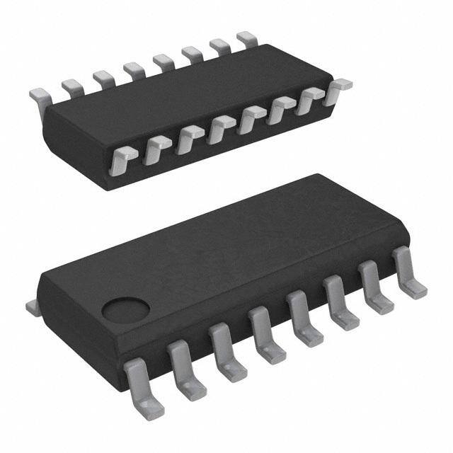
| 供应商器件封装 | 16-SOIC N |
| 其它名称 | 296-24674-1 |
| 制造商产品页 | http://www.ti.com/general/docs/suppproductinfo.tsp?distId=10&orderablePartNumber=TMS3705A1DRG4 |
| 包装 | 剪切带 (CT) |
| 封装/外壳 | 16-SOIC(0.154",3.90mm 宽) |
| 标准包装 | 1 |
| 特性 | - |
| 频率 | 134.2kHz |


- 商务部:美国ITC正式对集成电路等产品启动337调查
- 曝三星4nm工艺存在良率问题 高通将骁龙8 Gen1或转产台积电
- 太阳诱电将投资9.5亿元在常州建新厂生产MLCC 预计2023年完工
- 英特尔发布欧洲新工厂建设计划 深化IDM 2.0 战略
- 台积电先进制程称霸业界 有大客户加持明年业绩稳了
- 达到5530亿美元!SIA预计今年全球半导体销售额将创下新高
- 英特尔拟将自动驾驶子公司Mobileye上市 估值或超500亿美元
- 三星加码芯片和SET,合并消费电子和移动部门,撤换高东真等 CEO
- 三星电子宣布重大人事变动 还合并消费电子和移动部门
- 海关总署:前11个月进口集成电路产品价值2.52万亿元 增长14.8%


PDF Datasheet 数据手册内容提取
Product Sample & Technical Tools & Support & Folder Buy Documents Software Community TMS3705 SCBS881D–JANUARY2010–REVISEDOCTOBER2016 TMS3705 Transponder Base Station IC 1 Device Overview 1.1 Features 1 • BaseStationICforTI-RFid™RFIdentification • Short-CircuitProtection Systems • Diagnosis • DrivesAntenna • Sleep-ModeSupplyCurrent:0.2mA • SendsModulatedDatatoAntenna • DesignedforAutomotiveRequirements • DetectsandDemodulatesTransponderResponse • 16-PinSOIC(D)Package (FSK) 1.2 Applications • CarAccess • BuildingAccess • Immobilization • LivestockReader 1.3 Description The TMS3705 transponder base station IC is used to drive the antenna of a TI-RFid transponder system, to send data modulated on the antenna signal, and to detect and demodulate the response of the transponder.Theresponseofthetransponderisafrequencyshiftkeyed(FSK)signal.Thehighorlowbits are coded in two different high-frequency signals (134.2 kHz for low bits and 123 kHz for high bits, nominal). The transponder induces these signals in the antenna coil according an internally stored code. The energy that the transponder needs to send out the data is stored in a charge capacitor in the transponder. The antenna field charges this capacitor in a preceding charge phase. The IC has an interfacetoanexternalmicrocontroller. TherearetwoconfigurationsfortheclocksupplytoboththemicrocontrollerandthebasestationIC: 1. ThemicrocontrollerandbasestationICaresuppliedwithaclocksignalderivedfromonlyone resonator:Theresonatorisattachedtothemicrocontroller.ThebasestationICissuppliedwithaclock signaldrivenbythedigitalclockoutputofthemicrocontroller.Theclockfrequencyiseither4MHzor 2MHz,dependingontheselectedmicrocontrollertype. 2. Themicrocontrollerandthebasestationeachhavetheirownresonator. The base station IC has an on-chip PLL that generates a clock frequency of 16 MHz for internal clock supply only. Only TMS3705BDRG4 and TMS3705DDRQ1 are recommended in combination with AES transponder products (for example, TRPWS21GTEA or RF430F5xxx). TMS3705A1DRG4 cannot be used incombinationwithAEStransponderproducts. DeviceInformation(1) PARTNUMBER PACKAGE BODYSIZE(2) TMS3705A1DRG4 SOIC(16) 9.9mm×3.91mm TMS3705BDRG4 SOIC(16) 9.9mm×3.91mm TMS3705CDRQ1 SOIC(16) 9.9mm×3.91mm TMS3705DDRQ1 SOIC(16) 9.9mm×3.91mm (1) Forthemostcurrentpart,package,andorderinginformationforallavailabledevices,seethePackage OptionAddenduminSection9,orseetheTIwebsiteatwww.ti.com. (2) Thesizesshownhereareapproximations.Forthepackagedimensionswithtolerances,seethe MechanicalDatainSection9. 1 An IMPORTANT NOTICE at the end of this data sheet addresses availability, warranty, changes, use in safety-critical applications, intellectualpropertymattersandotherimportantdisclaimers.PRODUCTIONDATA.
TMS3705 SCBS881D–JANUARY2010–REVISEDOCTOBER2016 www.ti.com 1.4 Functional Block Diagram Figure1-1showsthefunctionalblockdiagram. VDD SCI Digital Demodulator Encoder Limiter Diagnosis Transponder A_TST Resonance-Frequency Measurement SCIO Bandpass 10k Power-On SFB Reset RFAmplifier Control Logic With TXCT Vref Mode Control Register SENSE D_TST Full Bridge VDDA PLL F_SEL ANT1 Predrivers Controlled Frequency Divider OSC2 ANT2 VSSA OSC1 VSS VSSB Copyright © 2016,Texas Instruments Incorporated Figure1-1.FunctionalBlockDiagram 2 DeviceOverview Copyright©2010–2016,TexasInstrumentsIncorporated SubmitDocumentationFeedback ProductFolderLinks:TMS3705
TMS3705 www.ti.com SCBS881D–JANUARY2010–REVISEDOCTOBER2016 Table of Contents 1 DeviceOverview......................................... 1 6.5 RF Amplifier......................................... 11 .............................................. ........................ 1.1 Features 1 6.6 Band-PassFilterandLimiter 12 ........................................... ............................................ 1.2 Applications 1 6.7 Diagnosis 12 ............................................ ..................................... 1.3 Description 1 6.8 Power-onReset 12 ............................ ................................... 1.4 FunctionalBlockDiagram 2 6.9 FrequencyDivider 12 2 Revision History......................................... 3 6.10 Digital Demodulator................................. 12 3 DeviceCharacteristics.................................. 4 6.11 TransponderResonance-FrequencyMeasurement 13 ..................................... ......................................... 3.1 RelatedProducts 4 6.12 SCIEncoder 13 4 TerminalConfigurationandFunctions.............. 5 6.13 Control Logic........................................ 14 .......................................... ............................................ 4.1 PinDiagram 5 6.14 TestPins 16 4.2 SignalDescriptions................................... 5 7 Applications,Implementation,andLayout........ 17 5 Specifications ............................................ 6 7.1 ApplicationDiagram................................. 17 5.1 AbsoluteMaximumRatings.......................... 6 8 DeviceandDocumentationSupport............... 18 .......................................... ..................... 5.2 ESDRatings 6 8.1 GettingStartedandNextSteps 18 ................ ............................... 5.3 RecommendedOperatingConditions 6 8.2 Device Nomenclature 18 ............................. ................................. 5.4 ElectricalCharacteristics 7 8.3 ToolsandSoftware 19 5.5 ThermalResistanceCharacteristicsforD(SOIC) 8.4 DocumentationSupport............................. 19 .............................................. Package 8 .............................. 8.5 CommunityResources 20 ............................. 5.6 Switching Characteristics 8 .......................................... 8.6 Trademarks 20 ..................................... 5.7 TimingDiagrams 9 ..................... 8.7 ElectrostaticDischargeCaution 20 6 DetailedDescription................................... 11 ............................... 8.8 ExportControlNotice 20 ....................................... 6.1 PowerSupply 11 ............................................. 8.9 Glossary 20 ............................................ 6.2 Oscillator 11 9 Mechanical,Packaging,andOrderable 6.3 Predrivers ........................................... 11 Information.............................................. 21 ........................................... 6.4 FullBridge 11 2 Revision History NOTE:Pagenumbersforpreviousrevisionsmaydifferfrompagenumbersinthecurrentversion. ChangesfromApril12,2016toOctober18,2016 Page • UpdatedthelastparagraphinSection1.3,Description......................................................................... 1 • AddedTMS3705CDRQ1intheDeviceInformationtable....................................................................... 1 • AddedSection3,DeviceCharacteristics ......................................................................................... 4 • Updatedtheparagraphthatstarts"TheTMS3705xDRG4canadjustthecarrierfrequency..."inSection6.13, ControlLogic......................................................................................................................... 16 • AddedTable7-1,BillofMaterials(BOM) ....................................................................................... 17 • ChangedtheorganizationofSection8,DeviceandDocumentationSupport.............................................. 18 • ChangedFigure8-1,DeviceNomenclature(addedsiliconrevCandQ100qualification)................................ 18 Copyright©2010–2016,TexasInstrumentsIncorporated RevisionHistory 3 SubmitDocumentationFeedback ProductFolderLinks:TMS3705
TMS3705 SCBS881D–JANUARY2010–REVISEDOCTOBER2016 www.ti.com 3 Device Characteristics Table3-1liststhecharacteristicsoftheTMS3705. Table3-1.DeviceCharacteristics Characteristic TMS3705 Datarate(maximum) 8kbps Frequency 134.2kHz Requiredantennainductance 100to1000µH Supplyvoltage 4.5to5.5Vdc Transmissionprinciple HDX,FSK 3.1 Related Products Forinformationaboutotherdevicesinthisfamilyofproductsorrelatedproducts,seethefollowinglinks. ProductsforWirelessConnectivity Connectmore–Industry’sbroadestwirelessconnectivityportfolio ProductsforNFC/RFID Texas Instruments provides one of the industry’s largest, most differentiated NFC product portfolios enabling lower power solutions to meet a broad range of RF connectivityneeds. CompanionProductsforTMS3705 Review products that are frequently purchased or used with this product. ReferenceDesigns The TI Designs Reference Design Library is a robust reference design library that spans analog, embedded processor, and connectivity. Created by TI experts to help you jump start your system design, all TI Designs include schematic or block diagrams, BOMs, anddesignfilestospeedyourtimetomarket. 4 DeviceCharacteristics Copyright©2010–2016,TexasInstrumentsIncorporated SubmitDocumentationFeedback ProductFolderLinks:TMS3705
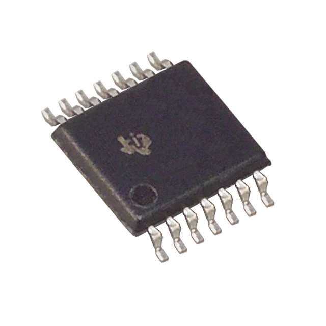
TMS3705 www.ti.com SCBS881D–JANUARY2010–REVISEDOCTOBER2016 4 Terminal Configuration and Functions 4.1 Pin Diagram Figure4-1showsthepinoutofthe16-pinD(SOIC)package. SENSE 1 16 TXCT SFB 2 15 F_SEL D_TST 3 14 SCIO A_TST 4 13 NC ANT1 5 12 VSS/VSSB VSSA 6 11 OSC1 ANT2 7 10 OSC2 VDDA 8 9 VDD NC–No connection Figure4-1.16-PinDPackage(TopView) 4.2 Signal Descriptions Table4-1describesthedevicesignals. Table4-1.SignalDescriptions TERMINAL TYPE DESCRIPTION NO. NAME 1 SENSE Analoginput InputoftheRFamplifier 2 SFB Analogoutput OutputoftheRFamplifier 3 D_TST Digitaloutput Testoutputfordigitalsignals 4 A_TST Analogoutput Testoutputforanalogsignals 5 ANT1 Driveroutput Antennaoutput1 6 VSSA Supplyinput Groundforthefullbridgedrivers 7 ANT2 Driveroutput Antennaoutput2 8 VDDA Supplyinput Voltagesupplyforthefullbridgedrivers 9 VDD Supplyinput Voltagesupplyfornonpowerblocks 10 OSC2 Analogoutput Oscillatoroutput 11 OSC1 Analoginput Oscillatorinput 12 VSS/VSSB Supplyinput GroundfornonpowerblocksandPLL 13 NC Notconnected 14 SCIO Digitaloutput Dataoutputtothemicrocontroller 15 F_SEL Digitalinput Controlinputforfrequencyselection(defaultvalueishigh) 16 TXCT Digitalinput Controlinputfromthemicrocontroller(defaultvalueishigh) Copyright©2010–2016,TexasInstrumentsIncorporated TerminalConfigurationandFunctions 5 SubmitDocumentationFeedback ProductFolderLinks:TMS3705
TMS3705 SCBS881D–JANUARY2010–REVISEDOCTOBER2016 www.ti.com 5 Specifications 5.1 Absolute Maximum Ratings(1) overoperatingfree-airtemperaturerange(unlessotherwisenoted) MIN MAX UNIT V Supplyvoltagerange VDD,VSS/VSSB,VDDA,VSSA –0.3 7 V DD V Voltagerange OSC1,OSC2 –0.3 V +0.3 V OSC DD V Voltagerange SCIO,TXCT,F_SEL,D_TST –0.3 V +0.3 V inout DD I Overloadclampingcurrent SCIO,TXCT,F_SEL,D_TST –5 5 mA inout V Outputvoltage ANT1,ANT2 –0.3 V +0.3 V ANT DD I Outputpeakcurrent ANT1,ANT2 –1.1 1.1 A ANT V Voltagerange SENSE,SFB,A_TST –0.3 V +0.3 V analog DD I SENSEinputcurrent SENSE,SFB,A_TST –5 5 mA SENSE I Inputcurrentincaseofovervoltage SFB –5 5 mA SFB T Operatingambienttemperature –40 85 °C A T Storagetemperature –55 150 °C stg P TotalpowerdissipationatT =85°C 0.5 W D A (1) StressesbeyondthoselistedunderAbsoluteMaximumRatingsmaycausepermanentdamagetothedevice.Thesearestressratings only,andfunctionaloperationofthedeviceattheseoranyotherconditionsbeyondthoseindicatedunderRecommendedOperating Conditionsisnotimplied.Exposuretoabsolute-maximum-ratedconditionsforextendedperiodsmayaffectdevicereliability. 5.2 ESD Ratings VALUE UNIT V ESDprotection(MILSTD883) ±2000 V ESD 5.3 Recommended Operating Conditions MIN NOM MAX UNIT V Supplyvoltage VDD,VSS/VSSB,VDDA,VSSA 4.5 5 5.5 V DD f Oscillatorfrequency OSC1,OSC2 4 MHz osc V High-levelinputvoltage F_SEL,TXCT,OSC1 0.7V V IH DD TXCT,OSC1 0.3V DD V Low-levelinputvoltage V IL F_SEL 0.2V DD I High-leveloutputcurrent SCIO,D_TST –1 mA OH I Low-leveloutputcurrent SCIO,D_TST 1 mA OL 6 Specifications Copyright©2010–2016,TexasInstrumentsIncorporated SubmitDocumentationFeedback ProductFolderLinks:TMS3705
TMS3705 www.ti.com SCBS881D–JANUARY2010–REVISEDOCTOBER2016 5.4 Electrical Characteristics V =4.5Vto5.5V,f =4MHz,F_SEL=high,overoperatingfree-airtemperaturerange(unlessotherwisenoted) DD osc PARAMETER TESTCONDITIONS MIN TYP MAX UNIT PowerSupply(VDD,VSS/VSSB,VDDA,VSSA) SumofsupplycurrentsinChargephase, I Supplycurrent 8 20 mA DD withoutantennaload SumofsupplycurrentsinSleepstate, I Supplycurrent,Sleepstate 0.015 0.2 mA Sleep withoutI/Ocurrents Oscillator(OSC1,OSC2) g Transconductance f =4MHz,0.5V atOSC1 0.5 2 5 mA/V osc osc pp C InputcapacitanceatOSC1(1) 10 pF in C OutputcapacitanceatOSC2(1) 10 pF out LogicInputs(TXCT,F_SEL,OSC1) TXCT 120 500 R Pullupresistance kΩ pullup F_SEL 10 500 LogicOutputs(SCIO,D_TST) V High-leveloutputvoltage 0.8V V OH DD V Low-leveloutputvoltage 0.2V V OL DD Full-BridgeOutputs(ANT1,ANT2) Full-bridgeN-channelandP-channel ΣR Sumofdrain-sourceresistances 7 14 Ω ds_on MOSFETsatdrivercurrentI =50mA ant Dutycycle P-channelMOSFETsoffullbridge 38% 40% 42% Symmetryofpulsedurationsforthe t /t 96% 104.5% on1 on2 P‑channelMOSFETsoffullbridge I Thresholdforovercurrentprotection 220 1100 mA oc t Switch-offtimeofovercurrentprotection Shorttogroundwith3Ω 0.25 10 µs oc Delayforswitchingonthefullbridgeafteran t 2 2.05 2.1 ms doc overcurrent I Leakagecurrent 1 µA leak AnalogModule(SENSE,SFB,A_TST) I Inputcurrent SENSE,Inchargephase –2 2 mA SENSE V / DCreferencevoltageofRFamplifier,related DCREF 9.25% 10% 11% V toVDD DD At500kHzwithexternalcomponentsto GBW Gain-bandwidthproductofRFamplifier achieveavoltagegainofminimum4‑mV 2 MHz pp and5-mV inputsignal pp At134kHzwithexternalcomponentsto φ PhaseshiftofRFamplifier achieveavoltagegainof5-mV and 16 ° O pp 20‑mV inputsignal pp Peak-to-peakinputvoltageofbandpassat At134kHz(correspondstoaminimaltotal Vsfb whichthelimitercomparatorshouldtoggle(2) gainof1000) 5 mV f Lowercut-offfrequencyofband-passfilter(3) 24 60 100 kHz low f Highercut-offfrequencyofband-passfilter(3) 160 270 500 kHz high A_TSTpinusedasinput,D_TSTpinas ΔV Hysteresisoflimiter output,offsetleveldeterminedbyband-pass 25 50 135 mV hys stage Diagnosis(SENSE) I Currentthresholdforoperatingantenna(4) 80 240 µA diag (1) Specifiedbydesign (2) Specifiedbydesign;functionaltestdoneforinputvoltageof90mV . pp (3) Band-passfiltertestedatthreedifferentfrequencies:f =134kHzandgain>30dB;f =24kHz;f =500kHz.Attenuation<–3 mid low high dB(reference=measuredgainatf =134kHz). mid (4) InternalresistanceswitchedonandmuchlowerthanexternalSENSEresistance. Copyright©2010–2016,TexasInstrumentsIncorporated Specifications 7 SubmitDocumentationFeedback ProductFolderLinks:TMS3705
TMS3705 SCBS881D–JANUARY2010–REVISEDOCTOBER2016 www.ti.com Electrical Characteristics (continued) V =4.5Vto5.5V,f =4MHz,F_SEL=high,overoperatingfree-airtemperaturerange(unlessotherwisenoted) DD osc PARAMETER TESTCONDITIONS MIN TYP MAX UNIT Phase-LockedLoop(D_TST) f PLLfrequency 15.984 16 16.0166 MHz pll Δf/f JitterofthePLLfrequency 6% pll Power-OnReset(POR) V PORthresholdvoltage,rising V risingwithlowslope 1.9 3.5 V por_r DD V PORthresholdvoltage,falling V fallingwithlowslope 1.3 2.6 V por_f DD 5.5 Thermal Resistance Characteristics for D (SOIC) Package PARAMETER VALUE UNIT R Thermalresistance,junctiontoambient(1) 130 °C/W θJA (1) Thejunction-to-ambientthermalresistanceundernaturalconvectionisobtainedinasimulationonaJEDEC-standard,High-Kboard,as specifiedinJESD51-7,inanenvironmentdescribedinJESD51-2a. 5.6 Switching Characteristics V =4.5Vto5.5V,f =4MHz,F_SEL=high,overoperatingfree-airtemperaturerange(unlessotherwisenoted) DD osc PARAMETER TESTCONDITIONS MIN TYP MAX UNIT Fromstartoftheoscillatorafterpoweron TimeforTXCThightoinitializeanew t orwakingupuntilreachingtheIdlestate 2 2.05 2.2 ms initmin transmission (seeFigure5-1,Figure5-2,Figure5-3) DelaybetweenleavingIdlestateandstartof Normaloperation(seeFigure5-1, t 2 2.12 2.2 ms diag diagnosisbyteatSCIO Figure5-2,Figure5-3) Delaybetweenendofchargeorendof t programandstartoftransponderdatatransmit SeeFigure5-1,Figure5-2,Figure5-3. 3 ms R onSCIO t Writepulsepause SeeFigure5-5. 0.1 ms off SignaldelayonTXCTforcontrollingthefull t Writemode 73 79 85 µs dwrite bridge t NRZbitdurationformodecontrolregister SeeFigure5-4. 121 128 135 µs mcr t NRZbitdurationonSCIO Asynchronousmode(seeFigure5-6) 63 64 65 µs sci t LowsignaldelayonTXCTtostop Synchronousmode 128 800 µs dstop t TotalTXCTtimeforreadingdataonSCIO Synchronousmode(seeFigure5-7) 900 µs t_sync t TXCTperiodforshiftingdataonSCIO Synchronousmode(seeFigure5-7) 4 64 100 µs sync t LowphaseonTXCT Synchronousmode(seeFigure5-7) 2 32 t –2 µs L_sync sync t DatareadyforoutputafterSCIOgoeshigh Synchronousmode(seeFigure5-7) 1 127 µs ready 8 Specifications Copyright©2010–2016,TexasInstrumentsIncorporated SubmitDocumentationFeedback ProductFolderLinks:TMS3705
TMS3705 www.ti.com SCBS881D–JANUARY2010–REVISEDOCTOBER2016 5.7 Timing Diagrams TXCT SCIO Diagnostic Start byte byte Data bytes tinit tch tR tdiag Phase MCW Charge Response Initialize transmission NOTE: MCW=Modecontrolwrite(towriteintothemodecontrolregister) Figure5-1.DefaultMode(ReadOnly,NoWritingIntoModeControlRegister) TXCT SCIO Diagnostic Start byte byte Data bytes tinit tch tR tdiag Phase MCW Charge Response Initialize transmission NOTE: MCW=Modecontrolwrite(towriteintothemodecontrolregister) Figure5-2.Read-OnlyMode(WritingIntoModeControlRegister) TXCT SCIO Diagnostic Start byte byte Data bytes tinit tch tprog tR tdiag Phase MCW Charge Write Program Response Initialize transmission NOTE: MCW=Modecontrolwrite(towriteintothemodecontrolregister) Figure5-3.Write/ReadMode(WritingIntoModeControlRegister) Copyright©2010–2016,TexasInstrumentsIncorporated Specifications 9 SubmitDocumentationFeedback ProductFolderLinks:TMS3705
TMS3705 SCBS881D–JANUARY2010–REVISEDOCTOBER2016 www.ti.com TXCT tinit tmcr tmcr Phase Low Bit1 Bit2 Bit3 Bit4 Bit5 Bit6 Bit7 Charge Start Test bit bit Initialize transmission End transmission Figure5-4.ModeControlWriteProtocol(NRZCoding) TXCT t t t ch offH offL t t bitH bitL Phase Charge High bit Low Program Figure5-5.TransponderWriteProtocol SCIO LSB 1 2 3 4 5 6 MSB Start Stop bit bit tsci tsci Figure5-6.TransmissiononSCIOinAsynchronousMode(NRZCoding) SCIO LSB 1 2 3 4 5 6 MSB Byte Stop ready bit TXCT tready tsync tt_sync tsync tL_sync Shift data MCU reads data Figure5-7.TransmissiononSCIOinSynchronousMode(NRZCoding) (ForDiagnosisByteandDataBytes) 10 Specifications Copyright©2010–2016,TexasInstrumentsIncorporated SubmitDocumentationFeedback ProductFolderLinks:TMS3705
TMS3705 www.ti.com SCBS881D–JANUARY2010–REVISEDOCTOBER2016 6 Detailed Description 6.1 Power Supply The device is supplied with 5 V by an external voltage regulator through two supply pins, one for providing the driver current for the antenna and the analog part in front of the digital demodulator and one for supplyingtheotherblocks. The power supply supplies a power-on reset that brings the control logic into Idle state as soon as the supplyvoltagedropsunderacertainvalue. In Sleep state, the sum of both supply currents is reduced to 0.2 mA. The base station device falls into Sleep state 100 ms after TXCT has changed to high. When TXCT changes to low or is low, the base stationICimmediatelygoesintoandremainsinnormaloperation. 6.2 Oscillator The oscillator generates the clock of the base station IC of which all timing signals are derived. Between its input and output a crystal or ceramic resonator is connected that oscillates at a typical frequency of 4MHz.Ifadigitalclocksignalwithafrequencyof4MHzor2MHzissuppliedtopinOSC1,thesignalcan beusedtogeneratetheinternaloperationfrequencyof16MHz. The oscillator block contains a PLL that generates the internal clock frequency of 16 MHz from the input clock signal. The PLL multiplies the input clock frequency depending on the logic state of the input pin F_SELbyafactorof4(F_SELishigh)orbyafactorof8(F_SELislow). IntheSleepstate,theoscillatorisoff. 6.3 Predrivers The predrivers generate the signals for the four power transistors of the full bridge using the carrier frequency generated by the frequency divider. The gate signals of the P-channel power transistors (active low) have the same width (±1 cycle of the 16 MHz clock), the delay between one P-channel MOSFET being switched off and the other one being switched on is defined to be 12 cycles of the 16-MHz clock. In write mode the first activation of a gate signal after a bit pause is synchronized to the received transpondersignalbyaphaseshiftof18°. 6.4 Full Bridge The full bridge drives the antenna current at the carrier frequency during the charge phase and the active time of the write phase. The minimal load resistance the full bridge sees between its outputs in normal operation at the resonance frequency of the antenna is 43.3 Ω. When the full bridge is not active, the two driveroutputsareswitchedtoground. Bothoutputsofthefullbridgeareprotectedindependentlyagainstshortcircuitstoground. In case of an occurring short circuit, the full bridge is switched off in less than 10 µs to avoid a drop of the supply voltage. After a delay time of less than 10 ms the full bridge is switched on again to test if the short circuit is still there. An overcurrent due to a resistive short to ground that is higher than the maximum current in normal operation but lower than the current threshold for overcurrent protection does not need tobeconsidered. 6.5 RF Amplifier The RF amplifier is an operational amplifier with a fixed internal voltage reference and a voltage gain of 5 defined by external resistors. The RF amplifier has a high gain-bandwidth product of at least 2 MHz to show a phase shift of less than 16° for the desired signal and to give the possibility to use it as a low-pass filterbyadaptingadditionalexternalcomponents. The input signal of the RF amplifier is DC coupled to the antenna. The amplitude of the output signal of theRFamplifierishigherthan5mVpeak-to-peak. Copyright©2010–2016,TexasInstrumentsIncorporated DetailedDescription 11 SubmitDocumentationFeedback ProductFolderLinks:TMS3705
TMS3705 SCBS881D–JANUARY2010–REVISEDOCTOBER2016 www.ti.com 6.6 Band-Pass Filter and Limiter The band-pass filter provides amplification and filtering without external components. The lower cut-off frequency is approximately a factor of 2 lower than the average signal frequency of 130 kHz, the higher cut-offfrequencyisapproximatelyafactorof2higherthan130kHz. The limiter converts the analog sine-wave signal to a digital signal. The limiter provides a hysteresis depending on the minimal amplitude of its input signal. The duty cycle of its digital output signal is between40%and60%.Theband-passfilterandthelimitertogetherhaveahighgainofatleast1000. 6.7 Diagnosis The diagnosis is carried out during the charge phase to detect whether the full bridge and the antenna are working. When the full bridge drives the antenna, the voltage across the coil exceeds the supply voltage so that the voltage at the input of the RF amplifier is clamped by the ESD-protection diodes. For diagnosis, the SENSE pin is loaded on-chip with a switchable resistor to ground so that the internal switchable resistor and the external SENSE resistor form a voltage divider, while the internal resistor is switched off in read mode. When the voltage drop across the internal resistor exceeds a certain value, the diagnosis block passes the frequency of its input signal to the digital demodulator. The frequency of the diagnosis signal is accepted if eight subsequent times can be detected, all with their counter state within the range of 112 to 125, during the diagnosis time (at most 0.1 ms). The output signal is used only during thechargephase,otherwiseitisignored. When the short-circuit protection switches off one of the full-bridge drivers, the diagnosis also indicates an improper operation of the antenna by sending the same diagnostic byte to the microcontroller as for the otherfailuremode. During diagnosis, the antenna drivers are active. In synchronous mode the antenna drivers remain active up to 1 ms after the diagnosis is performed, without any respect to the logic state of the signal at TXCT (thusenablingthemicrocontrollertoclockoutthediagnosisbyte). 6.8 Power-on Reset The power-on reset generates an internal reset signal to allow the control logic to start up in the defined way. 6.9 Frequency Divider The frequency divider is a programmable divider that generates the carrier frequency for the full-bridge antenna drivers. The default value for the division factor is the value 119 needed to provide the nominal carrier frequency of 134.45 kHz generated from 16 MHz. The resolution for programming the division factor is one divider step that corresponds to a frequency shift of approximately 1.1 kHz. The different division factors needed to cover the range of frequencies for meeting the resonance frequency of the transponderare114to124. 6.10 Digital Demodulator The input signal of the digital demodulator comes from the limiter and is frequency-coded according to the high- and low-bit sequence of the transmitted transponder code. The frequency of the input signal is measured by counting the oscillation clock for the time period of the input signal. As the high-bit and low- bit frequencies are specified with wide tolerances, the demodulator is designed to distinguish the high-bit and the low-bit frequency by the shift between the two frequencies and not by the absolute values. The thresholdbetweenthehigh-bitandthelow-bitfrequencyisdefinedto be 6.5 kHz lower than the measured low-bitfrequencyandhasahysteresisof ±0.55kHz. 12 DetailedDescription Copyright©2010–2016,TexasInstrumentsIncorporated SubmitDocumentationFeedback ProductFolderLinks:TMS3705
TMS3705 www.ti.com SCBS881D–JANUARY2010–REVISEDOCTOBER2016 The demodulator is controlled by the control logic. After the charge phase (that is during read or write phase) it measures the time period of its input signal and waits for the transponder resonance-frequency measurement to determine the counter state for the threshold between high-bit and low-bit frequency. Then the demodulator waits for the occurrence of the start bit. For that purpose, the results of the comparisons between the measured time periods and the threshold are shifted in a 12-bit shift register. The detection of the start bit comes into effect when the contents of the shift register matches a specific pattern, indicating 8 subsequent periods below the threshold immediately followed by 4 subsequent periods above the threshold. A 2-period digital filter is inserted in front of the 12-bit shift register to make a start bit detection possible in case of a nonmonotonous progression of the time periods during a transition fromlow-tohigh-bitfrequency. The bit stream detected by the input stage of the digital demodulator passes a digital filter before being evaluated. After demodulation, the serial bit flow received from the transponder is buffered byte-wise beforebeingsenttothemicrocontrollerbySCIencoding. 6.11 Transponder Resonance-Frequency Measurement During the prebit reception phase, the bits the transponder transmits show the low-bit frequency, which is the resonance frequency of the transponder. The time periods of the prebits are evaluated by the demodulator counter. Based on the counter states, an algorithm is implemented that ensures a correct measurementoftheresonancefrequencyofthetransponder: 1. Atimeperiodofthelow-bitfrequencyhasacounterstatebetween112and125. 2. Themeasurementofthelow-bitfrequency(theaverageofeightsubsequentcounterstates)is acceptedduringthewritemode,whentheeighttimeperiodshavecounterstatesinthedefinedrange. ThemeasurementduringwritemodeisstartedwiththefallingedgeatTXCTusingthefixeddelaytime atwhichendthefullbridgeisswitchedonagain. 3. Thecounterstateofthemeasuredlow-bitfrequencyresultsintheaveragecounterstateofan acceptedmeasurementandcanbeusedtoupdatetheregisteroftheprogrammablefrequencydivider. 4. Themeasurementofthelow-bitfrequency(theaverageofeightsubsequentcounterstates)is acceptedduringthereadmode,whentheeighttimeperiodshavecounterstatesinthedefinedrange. Thestartofthemeasurementduringreadmodeisdelayedtouseastableinputsignalforthe measurement. 5. Thethresholdtodistinguishbetweenhigh-bitandlow-bitfrequencyiscalculatedtobebyavalueof5 or7(seehysteresisinthreshold)higherthanthecounterstateofthemeasuredlow-bitfrequency. 6.12 SCI Encoder An SCI encoder performs the data transmission to the microcontroller. As the transmission rate of the transponder is lower than the SCI transmission rate, the serial bit flow received from the transponder is bufferedafterdemodulationandbeforeSCIencoding. The SCI encoder uses an 8-bit shift register to send the received data byte-wise (least significant bit first) to the microcontroller with a transmission rate of 15.625 kbaud (±1.5 %), 1 start bit (high), 1 stop bit (low), and no parity bit (asynchronous mode indicated by the SYNC bit of the Mode Control register is permanently low). The data bits at the SCIO output are inverted with respect to the corresponding bits sentbythetransponder. The transmission starts after the reception of the start bit. The start byte detection is initialized with the first rising edge. Typical values for the start byte are 81_H or 01_H (at SCIO). The start byte is the first byte to be sent to the microcontroller. The transmission stops and the base station returns to the Idle state when TXCT becomes low or 20 ms after the beginning of the read phase. TXCT remains low for at least 128µstostopthereadphaseandlessthan900 µstoavoidstartingthenexttransmissioncycle. Copyright©2010–2016,TexasInstrumentsIncorporated DetailedDescription 13 SubmitDocumentationFeedback ProductFolderLinks:TMS3705
TMS3705 SCBS881D–JANUARY2010–REVISEDOCTOBER2016 www.ti.com The SCI encoder also sends the diagnostic byte 2 ms after beginning of the charge phase. In case of a normal operation of the antenna, the diagnostic byte AF_H is sent. If no antenna oscillation can be measured or if at least one of the full-bridge drivers is switched off due to a detected short circuit, the diagnosticbyteFF_Hissenttoindicatethefailuremode. The SCI encoder can be switched into a synchronous data transmission mode by setting the mode control register bit SYNC to high. In this mode, the output SCIO indicates by a high state that a new byte is ready to be transmitted. The microcontroller can receive the 8 bits at SCIO when sending the eight clock signals (fallingedgemeansactive)forthesynchronousdatatransmissionthroughpinTXCTtotheSCIencoder. 6.13 Control Logic The control logic is the core of the TMS3705 circuit. This circuit contains a sequencer or a state machine that controls the global operations of the base station (see Figure 6-1). This block has a default mode configuration but can also be controlled by the microcontroller through the TXCT serial input pin to change the configuration and to control the programmable frequency divider. For that purpose a mode control registerisimplementedinthismodulethatcanbewrittenbythemicrocontroller. 14 DetailedDescription Copyright©2010–2016,TexasInstrumentsIncorporated SubmitDocumentationFeedback ProductFolderLinks:TMS3705
TMS3705 www.ti.com SCBS881D–JANUARY2010–REVISEDOCTOBER2016 Power Sleep on Approximately 2 ms afterTXCTgoes low After approximately (see Note D) 2 ms After approximately 100 ms Idle TXCTis low TXCTgoes high before 96 µs 0.9 ms afterTXCTgoes low (see Note B) Mode Control Register or approximately 4 ms after start of Programming receive phase if no start bit is detected See Note C or otherwise approximately 20 ms Write bits into after start of receive phase mode control register See Note E Mode control register bits received Diagnosis Phase Receive Phase Start of charge phase, Frequency measurement, Perform diagnosis, Fail Transponder signal demodulation, Send diagnostic byte Data output to MCU after approximately 2 ms after reception of start byte leaving Idle state Diagnostic byte sent (see NoteA) TXCTremains high for 1.6 ms Write Phase Charge Phase (see Note F) TXCTgoes high Start of write phase, Charge phase continues Frequency measurement, Program phase A. InSCIsynchronousmode,thistransitionalways occursapproximately3 msafterleavingIdle state.Diagnostic byte transmissioniscompletebeforethetransition. B. AfallingedgeonTXCTinterruptsthereceivephaseafteradelayof0.9ms.TXCTmustremainlowforatleast128 µs.IfTXCTisstilllowafterthe0.9-msdelay,thebasestationenterstheIdlestateandthentheDiagnosisphaseone clockcyclelater(seethedottedlinemarkedwith"SeeNoteC").Nomodecontrolregistercanbewritten,andonlythe defaultmodeisfullysupportedinthiscase.Otherwise,ifTXCTreturnshighandremainshighduringthedelay,the base station stays in Idle state and waits for TXCT to go low (which properly starts a new mode control register programmingoperation)orwaitsfor100mstoentertheSleepstate. C. Thistransitionoccursonlyinaspecialcase,asdescribedinNoteB. D. AfallingedgeonTXCTinterruptstheSleepstate.Onlythedefaultmodeisfullysupportedwhenstartinganoperation fromtheSleepstatewithonlyonefallingedgeonTXCT,becauseofthe2-msdelay.Forpropermodecontrolregister programming,TXCTmustreturntohighandremainhighduringthisdelay. E. Idlestateisthenextstateincaseofundefinedstates(fail-safestatemachine). F. FrequencymeasurementisavailablefortheTMS3705A1DRG4only. Figure6-1.OperationalStateDiagramfortheControlLogic The default mode is a read-only mode that uses the default frequency as the carrier frequency for the full bridge.Thereforethemodecontrolregisterdoesnotneedtobewritten(itisfilledwithlowstates),andthe communication sequence between microcontroller and base station starts with TXCT being low for a fixed timetoinitiatethechargephase.WhenTXCTbecomeshighagain,themoduleentersthereadphaseand thedatatransmissionthroughtheSCIOpintothemicrocontrollerstarts. There is another read-only mode that differs from the default mode only in the writing of the mode control register before the start of the charge phase. The method to fill the mode control register and the meaning ofitscontentsisdescribedinthefollowingparagraphs. Copyright©2010–2016,TexasInstrumentsIncorporated DetailedDescription 15 SubmitDocumentationFeedback ProductFolderLinks:TMS3705
TMS3705 SCBS881D–JANUARY2010–REVISEDOCTOBER2016 www.ti.com The write-read mode starts with the programming of the mode control register. Then the charge phase starts with TXCT being low for a fixed time. When TXCT becomes high again, the write phase begins in which the data are transmitted from the microcontroller to the transponder through the TXCT pin, the control logic, the predrivers, and the full bridge by amplitude modulation of 100% with a fixed delay time. After the write phase TXCT goes low again to start another charge or program phase. When TXCT becomeshighagain,thereadphasebegins. The contents of the mode control register (see Table 6-1) define the mode and the way that the carrier frequency generated by the frequency divider is selected to meet the transponder resonance frequency as closelyaspossible. Table6-1.ModeControlRegister(7-BitRegister) BIT RESET DESCRIPTION NAME NO. VALUE START_BIT Bit0 0 START_BIT=0 Thestartbitisalwayslowanddoesnotneedtobestored. DATA_BIT[4:1]=0000 Microcontrollerselectsdivisionfactor119 DATA_BIT1 Bit1 0 DATA_BIT[4:1]=1111 Divisionfactorisadaptedautomatically(1) DATA_BIT[4:1]=0001 Microcontrollerselectsdivisionfactor114 DATA_BIT2 Bit2 0 DATA_BIT[4:1]=0010 Microcontrollerselectsdivisionfactor115 ... ... DATA_BIT3 Bit3 0 DATA_BIT[4:1]=0110 Microcontrollerselectsdivisionfactor119 ... ... DATA_BIT4 Bit4 0 DATA_BIT[4:1]=1011 Microcontrollerselectsdivisionfactor124 SCI_SYNC=0 Asynchronousdatatransmissiontothemicrocontroller SCI_SYNC Bit5 0 SCI_SYNC=1 Synchronousdatatransmissiontothemicrocontroller RX_AFC=0 Demodulatorthresholdisadaptedautomatically RX_AFC Bit6 0 RX_AFC=1 DemodulatorthresholdisdefinedbyDATA_BIT[4:1] TEST_BIT=0 Nofurthertestbytes TEST_BIT Bit7 0 TEST_BIT=1 Furthertestbytefollowsforspecialtestmodes (1) Onlyavailableincombinationwithnon-AEStransponders The TMS3705xDRG4 can adjust the carrier frequency to the transponder resonance frequency automatically by giving the counter state of the transponder resonance-frequency measurement directly to the frequency divider by setting the first 4 bits in high state. The other combinations of the first 4 bits allow the microcontroller to select the default carrier frequency or to use another frequency. The division factor canbeselectedtobebetween114and124. Some bits are included for testability reasons. The default value of these test bits for normal operation is low. Bit 7 (TEST_BIT) is low for normal operation; otherwise, the base station may enter one of the test modes. The control logic also controls the demodulator, the SCI encoder, the diagnosis, and the transmission of thediagnosisbyteduringthechargephase. The state diagram in Figure 6-1 shows the general behavior of the state machine (the state blocks drawn can contain more than one state). All given times are measured from the moment when the state is enteredifnotspecifiedotherwise. 6.14 Test Pins The IC has an analog test pin A_TST for the analog part of the receiver. The digital output pin D_TST is usedfortestingtheinternallogic.Connectingbothpinsisnotrequired. 16 DetailedDescription Copyright©2010–2016,TexasInstrumentsIncorporated SubmitDocumentationFeedback ProductFolderLinks:TMS3705
TMS3705 www.ti.com SCBS881D–JANUARY2010–REVISEDOCTOBER2016 7 Applications, Implementation, and Layout NOTE InformationinthefollowingApplicationssectionisnotpartoftheTIcomponentspecification, and TI does not warrant its accuracy or completeness. TI's customers are responsible for determining suitability of components for their purposes. Customers should validate and test theirdesignimplementationtoconfirmsystemfunctionality. 7.1 Application Diagram Figure7-1showsatypicalapplicationdiagram. TMS3705 1 16 SENSE TXCT TXCTInput R2 2 15 SFB F_SEL 3 D_TST SCIO 14 SCIO Output R1 4 13 A_TST NC L1 5 12 ANT1 VSS Antenna 6 11 C3 VSSA OSC1 Q1 C1 7 10 4 MHz C2 ANT2 OSC2 8 9 VDDA VDD 5 V C4 Ground Copyright © 2016,Texas Instruments Incorporated Figure7-1.ApplicationDiagram Table7-1liststhebillofmaterialsfortheapplicationinFigure7-1. Table7-1.BillofMaterials(BOM) COMPONENT VALUE COMMENTS R1 47kΩ R2 150kΩ 422µHat L1 Sumidapartnumber:Vogt5810504240 134kHz C1 3nF NPO,COG(highQtypes).Voltageratingmustbe100VorhigherdependingonQfactor. C2 220pF NPO C3 220pF NPO C4 22µF LowESR muRatapartnumber:CSTCR4M00G55B-R0.Seeresonatordatasheet(loadcapacitanceis Q1 4-MHzresonator important). Copyright©2010–2016,TexasInstrumentsIncorporated Applications,Implementation,andLayout 17 SubmitDocumentationFeedback ProductFolderLinks:TMS3705
TMS3705 SCBS881D–JANUARY2010–REVISEDOCTOBER2016 www.ti.com 8 Device and Documentation Support 8.1 Getting Started and Next Steps RFID products from TI provide the ultimate solution for a wide range of applications. With its patented HDX technology, TI RFID offers unmatched performance in read range, read rate and robustness. For moreinformation,seeOverviewforNFC/RFID. 8.2 Device Nomenclature To designate the stages in the product development cycle, TI assigns prefixes to the part numbers of devices.Eachdevicehasoneofthreeprefixes:X,P,ornull(noprefix)(forexample, TMS3705). Devicedevelopmentevolutionaryflow: X Experimental device that is not necessarily representative of the final device's electrical specificationsandmaynotuseproductionassemblyflow. P Prototype device that is not necessarily the final silicon die and may not necessarily meet finalelectricalspecifications. null Productionversionofthesilicondiethatisfullyqualified. XandPdevicesareshippedagainstthefollowingdisclaimer: "Developmentalproductisintendedforinternalevaluationpurposes." Production devices have been characterized fully, and the quality and reliability of the device have been demonstratedfully.TI'sstandardwarrantyapplies. Predictions show that prototype devices (X or P) have a greater failure rate than the standard production devices. TI recommends that these devices not be used in any production system because their expected end-usefailureratestillisundefined.Onlyqualifiedproductiondevicesaretobeused. TI device nomenclature also includes a suffix with the device family name. This suffix indicates the packagetype(forexample,D).Figure8-1providesalegendforreadingthecompletedevicename. For orderable part numbers of TMS3705 devices in the D package types, see the Package Option AddenduminSection9,theTIwebsite,orcontactyourTIsalesrepresentative. TMS3705 A D R G4 Family Qualification Revision Tape and Reel Packaging Family TMS3705 =Transponder base station IC Revision A1, B, C, D = Silicon revision Packaging http://www.ti.com/packaging Tape and Reel R = Large reel G4 = Green (RoHS and no Sb, Br) Qualification Q1 = Q100 Qualified Figure8-1.DeviceNomenclature 18 DeviceandDocumentationSupport Copyright©2010–2016,TexasInstrumentsIncorporated SubmitDocumentationFeedback ProductFolderLinks:TMS3705
TMS3705 www.ti.com SCBS881D–JANUARY2010–REVISEDOCTOBER2016 8.3 Tools and Software DesignKitsandEvaluationModules Low-FrequencyDemoReader The ADR2 Evaluation Kit contains a low-frequency reader required to evaluate and operate the TI Car Access products. The kit comes with a reader base board, LF antenna, and a USB-RS232 adapter. Together with the PC software available online, all functions of the reader can be controlled and all automotive transponders, remote keyless entry, and passive entry devices can be addressed. Operation of transponder functions and also passive entry communication is supported by the same system without component changes. PaLFI,PassiveLow-FrequencyEvaluationKitTMS37157 The PaLFI Evaluation kit contains all components required to evaluate and operate the TMS37157. The kit comes with an eZ430 MSP430F1612 USB development stick, and an MSP430 target board including an MSP430F2274 plus the TMS37157 PaLFI. A battery board for active operation in addition to anRFIDbasestationreader/writerprovidetheinfrastructureforvariousevaluationsetups. 8.4 Documentation Support Thefollowingdocumentationdescribesthetransponder,relatedperipherals,andothertechnicalcollateral. ReceivingNotificationofDocumentUpdates To receive notification of documentation updates—including silicon errata—go to the TMS3705 product folder.Intheupperrightcorner,clickthe"Alertme"button.Thisregistersyoutoreceiveaweeklydigestof productinformationthathaschanged(ifany).Forchangedetails,checktherevisionhistoryofanyrevised document. ApplicationReports ResonantTrimmingSequence This application report presents an efficient and precise method on how to achieve the desired resonant frequency of configuring the trim array with only a few iterationsandmeasuringtheresonantfrequency. TMS3705RangeExtenderPowerSolutionUsingUCC27424-Q1 This application report provides supplementary information about the TI 134.2-kHz RFID Base Station IC TMS3705x in combination with an external driver IC. In particular, the document shows a low cost and easy-to-implement solution to improve the communication distance between the transaction processor(TRP)andtheReaderunit. TMS3705PassiveAntennaSolution The TI low-frequency transponder technology provides the possibility to use a simple passive antenna in combination with various antenna cable lengths. This solution significantly reduces system costs because the active part of the transceiver can be added to the already existing host system; for example, the body control module(BCM)ofavehicle. IntegratedTIRISRFModuleTMS3705AIntroductiontoLowFrequencyReader A TIRIS setup consists of one or more Transponders and a Reader. The Reader described in this application note normally contains the Reader Antenna, the RF Module and the Control Module. MoreLiterature WirelessConnectivityTri-foldOverview At TI, we are committed to delivering a broad portfolio of wireless connectivity solutions which consume the lowest power and are the easiest to use. With TI innovation supporting your designs, you can share, monitor and manage data wirelesslyforapplicationsinwearables,homeandbuildingautomation,manufacturing,smart cities,healthcareandautomotive. MSP430™Ultra-Low-PowerMCUsandTI-RFidDevices The TI portfolio of MSP430 microcontrollers and TI-RFid devices is an ideal fit for low-power, robust RFID reader and transponder solutions. Together, MSP430 and TI-RFid devices help RF designers achieve low power consumption,best-in-classreadrangeandreliableperformanceatacompetitiveprice. Copyright©2010–2016,TexasInstrumentsIncorporated DeviceandDocumentationSupport 19 SubmitDocumentationFeedback ProductFolderLinks:TMS3705
TMS3705 SCBS881D–JANUARY2010–REVISEDOCTOBER2016 www.ti.com 8.5 Community Resources The following links connect to TI community resources. Linked contents are provided "AS IS" by the respective contributors. They do not constitute TI specifications and do not necessarily reflect TI's views; seeTI's TermsofUse. TIE2E™OnlineCommunity The TI engineer-to-engineer (E2E) community was created to foster collaboration among engineers. At e2e.ti.com, you can ask questions, share knowledge, exploreideasandhelpsolveproblemswithfellowengineers. TIEmbeddedProcessorsWiki Established to help developers get started with Embedded Processors from Texas Instruments and to foster innovation and growth of general knowledge about the hardwareandsoftwaresurroundingthesedevices. 8.6 Trademarks TI-RFid,MSP430,E2EaretrademarksofTexasInstruments. Allothertrademarksarethepropertyoftheirrespectiveowners. 8.7 Electrostatic Discharge Caution This integrated circuit can be damaged by ESD. Texas Instruments recommends that all integrated circuits be handled with appropriateprecautions.Failuretoobserveproperhandlingandinstallationprocedurescancausedamage. ESDdamagecanrangefromsubtleperformancedegradationtocompletedevicefailure.Precisionintegratedcircuitsmaybemore susceptibletodamagebecauseverysmallparametricchangescouldcausethedevicenottomeetitspublishedspecifications. 8.8 Export Control Notice Recipient agrees to not knowingly export or re-export, directly or indirectly, any product or technical data (as defined by the U.S., EU, and other Export Administration Regulations) including software, or any controlled product restricted by other applicable national regulations, received from disclosing party under nondisclosure obligations (if any), or any direct product of such technology, to any destination to which such export or re-export is restricted or prohibited by U.S. or other applicable laws, without obtaining prior authorization from U.S. Department of Commerce and other competent Government authorities to the extentrequiredbythoselaws. 8.9 Glossary TIGlossary Thisglossarylistsandexplainsterms,acronyms,anddefinitions. 20 DeviceandDocumentationSupport Copyright©2010–2016,TexasInstrumentsIncorporated SubmitDocumentationFeedback ProductFolderLinks:TMS3705
TMS3705 www.ti.com SCBS881D–JANUARY2010–REVISEDOCTOBER2016 9 Mechanical, Packaging, and Orderable Information The following pages include mechanical, packaging, and orderable information. This information is the most current data available for the designated devices. This data is subject to change without notice and revisionofthisdocument.Forbrowser-basedversionsofthisdatasheet,refertotheleft-handnavigation. Copyright©2010–2016,TexasInstrumentsIncorporated Mechanical,Packaging,andOrderableInformation 21 SubmitDocumentationFeedback ProductFolderLinks:TMS3705
PACKAGE OPTION ADDENDUM www.ti.com 16-Jun-2018 PACKAGING INFORMATION Orderable Device Status Package Type Package Pins Package Eco Plan Lead/Ball Finish MSL Peak Temp Op Temp (°C) Device Marking Samples (1) Drawing Qty (2) (6) (3) (4/5) TMS3705A1DRG4 OBSOLETE SOIC D 16 TBD Call TI Call TI -40 to 85 TMS3705A TMS3705BDRG4 ACTIVE SOIC D 16 TBD Call TI Call TI -40 to 85 TMS3705B TMS3705CDRQ1 OBSOLETE SOIC D 16 TBD Call TI Call TI -40 to 85 TMS3705CQ1 TMS3705DDRQ1 ACTIVE SOIC D 16 2500 Green (RoHS CU NIPDAU Level-3-260C-168 HR -40 to 85 TMS3705DQ1 & no Sb/Br) (1) The marketing status values are defined as follows: ACTIVE: Product device recommended for new designs. LIFEBUY: TI has announced that the device will be discontinued, and a lifetime-buy period is in effect. NRND: Not recommended for new designs. Device is in production to support existing customers, but TI does not recommend using this part in a new design. PREVIEW: Device has been announced but is not in production. Samples may or may not be available. OBSOLETE: TI has discontinued the production of the device. (2) RoHS: TI defines "RoHS" to mean semiconductor products that are compliant with the current EU RoHS requirements for all 10 RoHS substances, including the requirement that RoHS substance do not exceed 0.1% by weight in homogeneous materials. Where designed to be soldered at high temperatures, "RoHS" products are suitable for use in specified lead-free processes. TI may reference these types of products as "Pb-Free". RoHS Exempt: TI defines "RoHS Exempt" to mean products that contain lead but are compliant with EU RoHS pursuant to a specific EU RoHS exemption. Green: TI defines "Green" to mean the content of Chlorine (Cl) and Bromine (Br) based flame retardants meet JS709B low halogen requirements of <=1000ppm threshold. Antimony trioxide based flame retardants must also meet the <=1000ppm threshold requirement. (3) MSL, Peak Temp. - The Moisture Sensitivity Level rating according to the JEDEC industry standard classifications, and peak solder temperature. (4) There may be additional marking, which relates to the logo, the lot trace code information, or the environmental category on the device. (5) Multiple Device Markings will be inside parentheses. Only one Device Marking contained in parentheses and separated by a "~" will appear on a device. If a line is indented then it is a continuation of the previous line and the two combined represent the entire Device Marking for that device. (6) Lead/Ball Finish - Orderable Devices may have multiple material finish options. Finish options are separated by a vertical ruled line. Lead/Ball Finish values may wrap to two lines if the finish value exceeds the maximum column width. Important Information and Disclaimer:The information provided on this page represents TI's knowledge and belief as of the date that it is provided. TI bases its knowledge and belief on information provided by third parties, and makes no representation or warranty as to the accuracy of such information. Efforts are underway to better integrate information from third parties. TI has taken and continues to take reasonable steps to provide representative and accurate information but may not have conducted destructive testing or chemical analysis on incoming materials and chemicals. TI and TI suppliers consider certain information to be proprietary, and thus CAS numbers and other limited information may not be available for release. Addendum-Page 1
PACKAGE OPTION ADDENDUM www.ti.com 16-Jun-2018 In no event shall TI's liability arising out of such information exceed the total purchase price of the TI part(s) at issue in this document sold by TI to Customer on an annual basis. Addendum-Page 2
None
None
IMPORTANTNOTICE TexasInstrumentsIncorporated(TI)reservestherighttomakecorrections,enhancements,improvementsandotherchangestoits semiconductorproductsandservicesperJESD46,latestissue,andtodiscontinueanyproductorserviceperJESD48,latestissue.Buyers shouldobtainthelatestrelevantinformationbeforeplacingordersandshouldverifythatsuchinformationiscurrentandcomplete. TI’spublishedtermsofsaleforsemiconductorproducts(http://www.ti.com/sc/docs/stdterms.htm)applytothesaleofpackagedintegrated circuitproductsthatTIhasqualifiedandreleasedtomarket.AdditionaltermsmayapplytotheuseorsaleofothertypesofTIproductsand services. ReproductionofsignificantportionsofTIinformationinTIdatasheetsispermissibleonlyifreproductioniswithoutalterationandis accompaniedbyallassociatedwarranties,conditions,limitations,andnotices.TIisnotresponsibleorliableforsuchreproduced documentation.Informationofthirdpartiesmaybesubjecttoadditionalrestrictions.ResaleofTIproductsorserviceswithstatements differentfromorbeyondtheparametersstatedbyTIforthatproductorservicevoidsallexpressandanyimpliedwarrantiesforthe associatedTIproductorserviceandisanunfairanddeceptivebusinesspractice.TIisnotresponsibleorliableforanysuchstatements. BuyersandotherswhoaredevelopingsystemsthatincorporateTIproducts(collectively,“Designers”)understandandagreethatDesigners remainresponsibleforusingtheirindependentanalysis,evaluationandjudgmentindesigningtheirapplicationsandthatDesignershave fullandexclusiveresponsibilitytoassurethesafetyofDesigners'applicationsandcomplianceoftheirapplications(andofallTIproducts usedinorforDesigners’applications)withallapplicableregulations,lawsandotherapplicablerequirements.Designerrepresentsthat,with respecttotheirapplications,Designerhasallthenecessaryexpertisetocreateandimplementsafeguardsthat(1)anticipatedangerous consequencesoffailures,(2)monitorfailuresandtheirconsequences,and(3)lessenthelikelihoodoffailuresthatmightcauseharmand takeappropriateactions.DesigneragreesthatpriortousingordistributinganyapplicationsthatincludeTIproducts,Designerwill thoroughlytestsuchapplicationsandthefunctionalityofsuchTIproductsasusedinsuchapplications. TI’sprovisionoftechnical,applicationorotherdesignadvice,qualitycharacterization,reliabilitydataorotherservicesorinformation, including,butnotlimitedto,referencedesignsandmaterialsrelatingtoevaluationmodules,(collectively,“TIResources”)areintendedto assistdesignerswhoaredevelopingapplicationsthatincorporateTIproducts;bydownloading,accessingorusingTIResourcesinany way,Designer(individuallyor,ifDesignerisactingonbehalfofacompany,Designer’scompany)agreestouseanyparticularTIResource solelyforthispurposeandsubjecttothetermsofthisNotice. TI’sprovisionofTIResourcesdoesnotexpandorotherwisealterTI’sapplicablepublishedwarrantiesorwarrantydisclaimersforTI products,andnoadditionalobligationsorliabilitiesarisefromTIprovidingsuchTIResources.TIreservestherighttomakecorrections, enhancements,improvementsandotherchangestoitsTIResources.TIhasnotconductedanytestingotherthanthatspecifically describedinthepublisheddocumentationforaparticularTIResource. Designerisauthorizedtouse,copyandmodifyanyindividualTIResourceonlyinconnectionwiththedevelopmentofapplicationsthat includetheTIproduct(s)identifiedinsuchTIResource.NOOTHERLICENSE,EXPRESSORIMPLIED,BYESTOPPELOROTHERWISE TOANYOTHERTIINTELLECTUALPROPERTYRIGHT,ANDNOLICENSETOANYTECHNOLOGYORINTELLECTUALPROPERTY RIGHTOFTIORANYTHIRDPARTYISGRANTEDHEREIN,includingbutnotlimitedtoanypatentright,copyright,maskworkright,or otherintellectualpropertyrightrelatingtoanycombination,machine,orprocessinwhichTIproductsorservicesareused.Information regardingorreferencingthird-partyproductsorservicesdoesnotconstitutealicensetousesuchproductsorservices,orawarrantyor endorsementthereof.UseofTIResourcesmayrequirealicensefromathirdpartyunderthepatentsorotherintellectualpropertyofthe thirdparty,oralicensefromTIunderthepatentsorotherintellectualpropertyofTI. TIRESOURCESAREPROVIDED“ASIS”ANDWITHALLFAULTS.TIDISCLAIMSALLOTHERWARRANTIESOR REPRESENTATIONS,EXPRESSORIMPLIED,REGARDINGRESOURCESORUSETHEREOF,INCLUDINGBUTNOTLIMITEDTO ACCURACYORCOMPLETENESS,TITLE,ANYEPIDEMICFAILUREWARRANTYANDANYIMPLIEDWARRANTIESOF MERCHANTABILITY,FITNESSFORAPARTICULARPURPOSE,ANDNON-INFRINGEMENTOFANYTHIRDPARTYINTELLECTUAL PROPERTYRIGHTS.TISHALLNOTBELIABLEFORANDSHALLNOTDEFENDORINDEMNIFYDESIGNERAGAINSTANYCLAIM, INCLUDINGBUTNOTLIMITEDTOANYINFRINGEMENTCLAIMTHATRELATESTOORISBASEDONANYCOMBINATIONOF PRODUCTSEVENIFDESCRIBEDINTIRESOURCESOROTHERWISE.INNOEVENTSHALLTIBELIABLEFORANYACTUAL, DIRECT,SPECIAL,COLLATERAL,INDIRECT,PUNITIVE,INCIDENTAL,CONSEQUENTIALOREXEMPLARYDAMAGESIN CONNECTIONWITHORARISINGOUTOFTIRESOURCESORUSETHEREOF,ANDREGARDLESSOFWHETHERTIHASBEEN ADVISEDOFTHEPOSSIBILITYOFSUCHDAMAGES. UnlessTIhasexplicitlydesignatedanindividualproductasmeetingtherequirementsofaparticularindustrystandard(e.g.,ISO/TS16949 andISO26262),TIisnotresponsibleforanyfailuretomeetsuchindustrystandardrequirements. WhereTIspecificallypromotesproductsasfacilitatingfunctionalsafetyorascompliantwithindustryfunctionalsafetystandards,such productsareintendedtohelpenablecustomerstodesignandcreatetheirownapplicationsthatmeetapplicablefunctionalsafetystandards andrequirements.Usingproductsinanapplicationdoesnotbyitselfestablishanysafetyfeaturesintheapplication.Designersmust ensurecompliancewithsafety-relatedrequirementsandstandardsapplicabletotheirapplications.DesignermaynotuseanyTIproductsin life-criticalmedicalequipmentunlessauthorizedofficersofthepartieshaveexecutedaspecialcontractspecificallygoverningsuchuse. Life-criticalmedicalequipmentismedicalequipmentwherefailureofsuchequipmentwouldcauseseriousbodilyinjuryordeath(e.g.,life support,pacemakers,defibrillators,heartpumps,neurostimulators,andimplantables).Suchequipmentincludes,withoutlimitation,all medicaldevicesidentifiedbytheU.S.FoodandDrugAdministrationasClassIIIdevicesandequivalentclassificationsoutsidetheU.S. TImayexpresslydesignatecertainproductsascompletingaparticularqualification(e.g.,Q100,MilitaryGrade,orEnhancedProduct). Designersagreethatithasthenecessaryexpertisetoselecttheproductwiththeappropriatequalificationdesignationfortheirapplications andthatproperproductselectionisatDesigners’ownrisk.Designersaresolelyresponsibleforcompliancewithalllegalandregulatory requirementsinconnectionwithsuchselection. DesignerwillfullyindemnifyTIanditsrepresentativesagainstanydamages,costs,losses,and/orliabilitiesarisingoutofDesigner’snon- compliancewiththetermsandprovisionsofthisNotice. MailingAddress:TexasInstruments,PostOfficeBox655303,Dallas,Texas75265 Copyright©2018,TexasInstrumentsIncorporated