ICGOO在线商城 > 分立半导体产品 > 晶闸管 - TRIAC > Q6040K7TP
 Datasheet下载
- 型号: Q6040K7TP
- 制造商: Littelfuse
- 库位|库存: xxxx|xxxx
- 要求:
| 数量阶梯 | 香港交货 | 国内含税 |
| +xxxx | $xxxx | ¥xxxx |
查看当月历史价格
查看今年历史价格
Q6040K7TP产品简介:
ICGOO电子元器件商城为您提供Q6040K7TP由Littelfuse设计生产,在icgoo商城现货销售,并且可以通过原厂、代理商等渠道进行代购。 Q6040K7TP价格参考。LittelfuseQ6040K7TP封装/规格:晶闸管 - TRIAC, TRIAC Alternistor - Snubberless 600V 40A Through Hole TO-218 Isolated Tab。您可以下载Q6040K7TP参考资料、Datasheet数据手册功能说明书,资料中有Q6040K7TP 详细功能的应用电路图电压和使用方法及教程。
Littelfuse Inc.生产的型号为Q6040K7TP的晶闸管(TRIAC)是一种双向三端交流开关器件,广泛应用于各种需要控制交流电力的场景。以下是该型号的主要应用场景:

 1. 家用电器控制
   - 调光器:用于调节灯光亮度,通过相位控制改变输入到灯具的电压波形。
   - 风扇速度控制:用于调节电风扇或其他电机的速度。
   - 温度控制:在电热设备(如电烤箱、电饭煲等)中,作为功率控制器实现温度调节。

 2. 工业自动化
   - 电机启动与调速:用于控制小型交流电机的启动和运行速度。
   - 加热系统:在工业加热设备中,通过脉冲宽度调制(PWM)或相位控制调节加热功率。
   - 固态继电器(SSR):作为核心开关元件,用于替代传统机械继电器,实现更快速、更可靠的开关操作。

 3. 消费电子
   - 家电遥控:在需要远程控制功率输出的设备中,如空调、洗衣机等。
   - 电源管理:用于开关电源中的负载控制或保护电路。

 4. 照明系统
   - LED调光:尽管LED通常使用直流供电,但在某些交流驱动的LED系统中,TRIAC可用于调光。
   - 白炽灯/卤素灯调光:传统的调光应用中,TRIAC是核心元件。

 5. 汽车电子
   - 电动车窗和座椅调节:用于控制电机的启动和停止。
   - 车载加热器:在一些车辆的加热系统中,TRIAC用于调节加热功率。

 6. 其他应用
   - 舞台灯光控制:在娱乐行业中,用于调节舞台灯光的亮度和效果。
   - 太阳能逆变器:在某些小型逆变器中,TRIAC可用于控制交流输出。

 技术特点
Q6040K7TP具有较高的电流承载能力和耐压能力(额定电流为40A,阻断电压为600V),适合中高功率的应用场景。其紧凑的TO-223-3封装形式也便于集成到各种电路设计中。

总之,Q6040K7TP适用于需要高效、可靠交流电力控制的场合,尤其在需要频繁开关或调节功率的应用中表现出色。
| 参数 | 数值 |
| 产品目录 | |
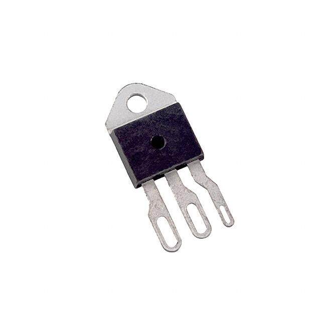
| 描述 | TRIAC ALTERNISTOR 600V 40A TO218双向可控硅 Altnstr 600V 40A Iso 100-100-100mA |
| 产品分类 | 双向可控硅分离式半导体 |
| GateTriggerCurrent-Igt | 100 mA |
| GateTriggerVoltage-Vgt | 2.5 V |
| 品牌 | Littelfuse Inc |
| 产品手册 | |
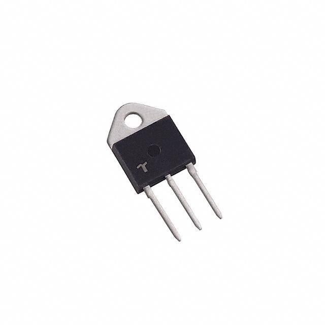
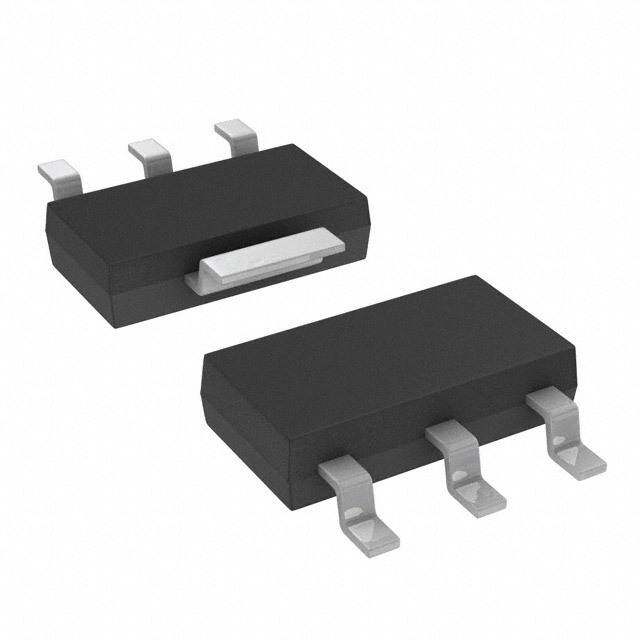
| 产品图片 |
|
| rohs | 符合RoHS无铅 / 符合限制有害物质指令(RoHS)规范要求 |
| 产品系列 | 晶体闸流管,双向可控硅,Littelfuse Q6040K7TP- |
| 数据手册 | |
| 产品型号 | Q6040K7TP |
| 三端双向可控硅类型 | 可控硅 - 无缓冲器 |
| 不重复通态电流 | 335 A, 400 A |
| 产品目录页面 | |
| 产品种类 | 双向可控硅 |
| 供应商器件封装 | TO-218 隔离的标片 |
| 保持电流Ih最大值 | 120 mA |
| 关闭状态漏泄电流(在VDRMIDRM下) | 200 uA |
| 其它名称 | Q6040K7 |
| 包装 | 管件 |
| 商标 | Littelfuse |
| 安装类型 | 通孔 |
| 安装风格 | Through Hole |
| 封装 | Tube |
| 封装/外壳 | TO-218-3(隔离式),TO-218AC |
| 封装/箱体 | TO-218-3 |
| 工厂包装数量 | 250 |
| 开启状态RMS电流-ItRMS | 40 A |
| 开启状态电压 | 1.8 V |
| 最大工作温度 | + 125 C |
| 最小工作温度 | - 40 C |
| 栅极触发电压-Vgt | 2.5 V |
| 栅极触发电流-Igt | 100 mA |
| 标准包装 | 25 |
| 电压-断态 | 600V |
| 电压-栅极触发(Vgt)(最大值) | 2V |
| 电流-不重复浪涌50、60Hz(Itsm) | 335A,400A |
| 电流-保持(Ih)(最大值) | 100mA |
| 电流-栅极触发(Igt)(最大值) | 100mA |
| 电流-通态(It(RMS))(最大值) | 40A |
| 系列 | Qxx40xx |
| 配置 | 单一 |
| 额定重复关闭状态电压VDRM | 600 V |


- 商务部:美国ITC正式对集成电路等产品启动337调查
- 曝三星4nm工艺存在良率问题 高通将骁龙8 Gen1或转产台积电
- 太阳诱电将投资9.5亿元在常州建新厂生产MLCC 预计2023年完工
- 英特尔发布欧洲新工厂建设计划 深化IDM 2.0 战略
- 台积电先进制程称霸业界 有大客户加持明年业绩稳了
- 达到5530亿美元!SIA预计今年全球半导体销售额将创下新高
- 英特尔拟将自动驾驶子公司Mobileye上市 估值或超500亿美元
- 三星加码芯片和SET,合并消费电子和移动部门,撤换高东真等 CEO
- 三星电子宣布重大人事变动 还合并消费电子和移动部门
- 海关总署:前11个月进口集成电路产品价值2.52万亿元 增长14.8%


PDF Datasheet 数据手册内容提取
Thyristors 40 Amp Alternistor (High Commutation) and Standard Triacs Qxx40xx Series RoHS Description The 40 Amp bi-directional solid state switch series is designed for AC switching and phase control applications such as motor speed, temperature modulation controls, lighting controls, and static switching relays. Alternistor type components only operate in quadrants I, II, & III and are used in circuits requiring high dv/dt capability. Standard type devices operate in quadrants I,II,III & IV. Agency Approval Features & Benefits • R oHS Compliant • S urge capability up to Agency Agency File Number 400A • G lass – passivated E71639* junctions • E lectrically isolated * - K and J Packages • V oltage capability up to K & J -Packages are UL Recognized for 2500Vrms 1000V Main Features Applications Excellent for AC switching and phase control applications Symbol Value Unit such as heating, lighting, and motor speed controls. I 40 A T(RMS) Typical applications are AC solid-state switches, industrial V /V 400 to 1000 V DRM RRM power tools, exercise equipment, white goods and I 35 to 100 mA commercial appliances. GT (Q1) Alternistor Triacs (no snubber required) are used in applications with extremely inductive loads requiring Schematic Symbol highest commutation performance. Internally constructed isolated packages are offered for MT2 ease of heat sinking with highest isolation voltage. G MT1 ©2008 Littelfuse, Inc. Specifications are subject to change without notice. Revised: 12/04/18
Thyristors 40 Amp Alternistor (High Commutation) and Standard Triacs Absolute Maximum Ratings – Alternistor Triac (3 Quadrants) Symbol Parameter Value Unit Qxx40x7 I RMS on-state current (full sine wave) T = 75 °C 40 A T(RMS) Qxx40xH6 C Non repetitive surge peak on-state current f = 50 Hz t = 20 ms 335 I A TSM (full cycle, TJ initial = 25°C) f = 60 Hz t = 16.7 ms 400 I2t I2t Value for fusing t = 8.3 ms 664 A2s p Critical rate of rise of on-state current di/dt f = 120 Hz T = 125 °C 150 A/μs (IG = 2 x IGT, tr ≤ 100 ns) J I Peak gate trigger current t=20μs T = 125 °C 4 A GTM p J P Average gate power dissipation T = 125 °C 0.5 W G(AV) J T Storage temperature range -40 to 150 °C stg T Operating junction temperature range -40 to 125 °C J Absolute Maximum Ratings – Standard Triac (4 Quadrants) Symbol Parameter Test Conditions Value Unit I RMS on-state current Qxx40x3/Qxx40x4 T = 75 °C 40 A T(RMS) C f = 50 Hz t = 20 ms 335 I Peak non-repetitive surge current A TSM f = 60 Hz t = 16 ms 400 I2t I2t Value for fusing t = 8.3 ms 664 A2s p di/dt Critical rate-of-rise of on-state current f = 120 Hz; T =125 °C 150 A/μs J I Peak gate current t=20μs T = 125 °C 4 A GTM p J P Average gate power dissipation T = 125°C 0.5 W G(AV) J T Storage temperature range -40 to 150 °C stg T Operating junction temperature range -40 to 125 °C J ©2008 Littelfuse, Inc. Specifications are subject to change without notice. Revised: 12/04/18
Thyristors 40 Amp Alternistor (High Commutation) and Standard Triacs Electrical Characteristics (T = 25°C, unless otherwise specified) — Alternistor Triac (3 Quadrants) J Value Symbol Test Conditions Quadrant Unit Qxx40xH6 Qxx40K5 Qxx40x7 I V = 12V R = 60 Ω I – II – III MAX. 80 50 100 mA GT D L V V = 12V R = 60 Ω I – II – III MAX. 1.3 1.3 2.0 V GT D L V V = V R = 3.3 kΩ T = 125°C I – II – III MIN. 0.2 V GD D DRM L J I I = 400mA MAX. 80 75 100 mA H T 400V 600 500 700 V = V Gate Open T = 125°C 600V 500 475 625 D DRM J dv/dt MIN. V/μs 800V 475 400 575 V = V Gate Open T = 100°C 1000V - - 500 D DRM J (dv/dt)c (di/dt)c = 21.6 A/ms T = 125°C MIN. 30 20 50 V/µs J t I = 2 x I PW = 15µs I = 56.6A(pk) TYP. 5 µs gt G GT T Electrical Characteristics (T = 25°C, unless otherwise specified) — Standard Triac (4 Quadrants) J Value Symbol Test Conditions Quadrant Qxx40x3 Unit Qxx40x4 I – II – III MAX. 35 50 I V = 12 V; R = 60 Ω mA GT D L IV MAX. 70 100 V V = 12 V; R = 60 Ω ALL MAX. 1.3 1.3 V GT D L V V = V ; R = 3.3 kΩ ; T = 125 °C ALL MIN. 0.2 0.2 V GD D DRM L J I I = 400mA (initial) MAX. 80 80 mA H T 400V 400 400 dv/dt V = V ; Gate Open; T = 125 °C 600V MIN. 400 400 V/μs D DRM J 800V 400 400 (dv/dt)c (di/dt)c = 4.3 A/ms; T = 125 °C MIN. 10 10 V/μs J t I = 2 x I ; PW = 15µs; I = 35.4 A TYP. 5 5 μs gt G GT T Static Characteristics Symbol Test Conditions Value Unit V I = 56.6A t = 380 µs T = 25°C MAX. 1.8 V TM TM p J T = 25°C 400 –1000V MAX. 20 μA J I DRM V = V / V T = 125°C 400 – 800V MAX. 5 mA I D DRM RRM J RRM T = 100°C 1000V MAX. 5 mA J ©2008 Littelfuse, Inc. Specifications are subject to change without notice. Revised: 12/04/18
Thyristors 40 Amp Alternistor (High Commutation) and Standard Triacs Thermal Resistances Symbol Parameter Value Unit Qxx40KH6 Qxx40K5/7 0.97 Qxx40K4 R Junction to case (AC) Qxx40K3 °C/W Ɵ(J-C) Qxx40JH6 0.95 Qxx40J7 Note: xx = voltage Figure 2: Normalized DC Gate Trigger Current for Figure 1: Definition of Quadrants All Quadrants vs. Junction Temperature ALL POLARITIES ARE REFERENCED TO MT1 4.0 MT2 POSITIVE (Positive Half Cycle) MT2 + MT2 C) (-)GIGATTE (+)IGGATTE = 25° 3.0 T J IGT - RMETF2MT1 QQIIIII QQIIV RMETFM2T1+ IGT atio of I/ I (GT GT 12..00 R (-)IGT (+)IGT GATE GATE 0.0 MT1 - MT1 -40 -15 10 35 60 85 110 +125 REF MT2 NEGATIVE REF Junction Temperature -- (°C) (Negative Half Cycle) Note: Alternistors will notN oOpTerEa:t eA linte QrnIVistors will not operate in QIV Figure 3: Normalized DC Holding Current Figure 4: Normalized DC Gate Trigger Voltage for vs. Junction Temperature All Quadrants vs. Junction Temperature 4.0 2.0 C) C) 3.0 25° 1.5 5° = of I / I (T = 2IHIHJ 2.0 o of V/ V (T GT GTJ 1.0 atio 1.0 Rati 0.5 R 0.0 0.0 -40- 15 10 35 60 85 110 +125 + 125 -40 -15 10 35 60 85 110 Junction Temperature - °C Junction Temperature - °C ©2008 Littelfuse, Inc. Specifications are subject to change without notice. Revised: 12/04/18
Thyristors 40 Amp Alternistor (High Commutation) and Standard Triacs Figure 5: Power Dissipation (Typical) Figure 6: Maximum Allowable Case Temperature vs. RMS On-State Current vs. On-State Current n 45 130 o ge On-State Power Dissipati] - Watts [PD (AV)11223340505050 x Allowable Case Temperature (T) - ºCC111789012000000 a a er 5 M 60 v A 0 50 0 4 8 12 16 20 24 28 32 36 40 0 5 10 15 20 25 30 35 40 45 50 RMS On-State Current [I ] - AMPS RMS On-State Current [I ] - AMPS T(RMS) T(RMS) Figure 7: On-State Current vs. On-State Voltage (Typical) 90 s 80 neouPS70 TC = 25ºC aM ntA gative Insta) - urrent (iT456000 eC e or NState 30 sitivOn-20 o P 10 0 0.6 0.8 1.0 1.2 1.4 1.6 Positive or Negative Instantaneous On-State Voltage (v) - Volts T Figure 8: Surge Peak On-State Current vs. Number of Cycles 1000 Supply Frequency: 60Hz Sinusoidal nt Load: Resistive e urr RMS On-State [IT(RMS)]: Max Rated Value at C Specific Case Temperature e at St Notes: ve) On-mps100 1) Gimamtee cdoiantterolyl mfolaloyw bien glo ssut rdguer icnugr raenndt interval. n-repetiti(I) – ATSM 2) Otreavtmeedprl eovraaadltu umer.ea yh anso tr ebteu rrneepde atote sdt euandtiyl -jsutnacteti o n o 10 N e ( g ur S k a e P 1 1 10 100 1000 Surge Current Duration – Full Cycles ©2008 Littelfuse, Inc. Specifications are subject to change without notice. Revised: 12/04/18
Thyristors 40 Amp Alternistor (High Commutation) and Standard Triacs Soldering Parameters Reflow Condition Pb – Free assembly tP T P - Temperature Min (T ) 150°C s(min) e RRaammpp--uupp Pre Heat -- TTeimmep e(mraitnu rteo Mmaaxx )( T(tss(m)ax)) 2600 0–° C180 secs rutarep TS(mTaxL) tL Average ramp up rate (Liquidus Temp) m PPrreehheeaatt RRaammpp--ddoown 5°C/second max e (T) to peak T L TS(min) T to T - Ramp-up Rate 5°C/second max tS S(max) L - Temperature (T) (Liquidus) 217°C Reflow L 25 - Time (min to max) (t) 60 – 150 seconds time to peak temperature s Time Peak Temperature (T) 260+0/-5 °C P Time within 5°C of actual peak 20 – 40 seconds Temperature (t) p Environmental Specifications Ramp-down Rate 5°C/second max Time 25°C to peak Temperature (T) 8 minutes Max. Test Specifications and Conditions P Do not exceed 280°C MIL-STD-750, M-1040, Cond A Applied AC Blocking Peak AC voltage @ 125°C for 1008 hours MIL-STD-750, M-1051, Temperature Cycling 100 cycles; -40°C to +150°C; 15-min dwell-time Physical Specifications EIA / JEDEC, JESD22-A101 Temperature/ 1008 hours; 320V - DC: 85°C; 85% Terminal Finish 100% Matte Tin-plated. Humidity rel humidity MIL-STD-750, M-1031, UL Recognized compound meeting High Temp Storage Body Material 1008 hours; 150°C flammability rating V-0 Low-Temp Storage 1008 hours; -40°C Lead Material Copper Alloy Resistance to MIL-STD-750 Method 2031 Solder Heat Solderability ANSI/J-STD-002, category 3, Test A Design Considerations Lead Bend MIL-STD-750, M-2036 Cond E Careful selection of the correct component for the application’s operating parameters and environment will go a long way toward extending the operating life of the Thyristor. Good design practice should limit the maximum continuous current through the main terminals to 75% of the component rating. Other ways to ensure long life for a power discrete semiconductor are proper heat sinking and selection of voltage ratings for worst case conditions. Overheating, overvoltage (including dv/dt), and surge currents are the main killers of semiconductors. Correct mounting, soldering, and forming of the leads also help protect against component damage. ©2008 Littelfuse, Inc. Specifications are subject to change without notice. Revised: 12/04/18
Thyristors 40 Amp Alternistor (High Commutation) and Standard Triacs Dimensions — TO-218X (J Package) — Isolated Mounting Tab C Inches Millimeters B D Dimension U DIA. Min Max Min Max A 0.810 0.835 20.57 21.21 MeasuremeTnct B 0.610 0.630 15.49 16.00 Point A C 0.178 0.188 4.52 4.78 F E Z D 0.055 0.070 1.40 1.78 E 0.487 0.497 12.37 12.62 F 0.635 0.655 16.13 16.64 MT1 W X G 0.022 0.029 0.56 0.74 J H 0.075 0.095 1.91 2.41 N Gate J 0.575 0.625 14.61 15.88 R K 0.256 0.264 6.50 6.71 T S M P G L 0.220 0.228 5.58 5.79 Y MT2 H M 0.080 0.088 2.03 2.24 K L N 0.169 0.177 4.29 4.49 V Note: Maximum torque to be applied to mounting tab P 0.034 0.042 0.86 1.07 is 8 in-lbs. (0.904 Nm). R 0.113 0.121 2.87 3.07 S 0.086 0.096 2.18 2.44 T 0.156 0.166 3.96 4.22 U 0.161 0.165 4.10 4.20 V 0.603 0.618 15.31 15.70 W 0.000 0.005 0.00 0.13 X 0.003 0.012 0.07 0.30 Y 0.028 0.032 0.71 0.81 Z 0.085 0.095 2.17 2.42 Dimensions — TO-218AC (K Package) — Isolated Mounting Tab Inches Millimeters TC Measurement Point Dimension B C Min Max Min Max U (diameter) D A 0.810 0.835 20.57 21.21 B 0.610 0.630 15.49 16.00 A C 0.178 0.188 4.52 4.78 F E D 0.055 0.070 1.40 1.78 W E 0.487 0.497 12.37 12.62 Gate F 0.635 0.655 16.13 16.64 P J G 0.022 0.029 0.56 0.74 MT1 H 0.075 0.095 1.91 2.41 MT2 M H J 0.575 0.625 14.61 15.88 Q G K 0.211 0.219 5.36 5.56 R N L 0.422 0.437 10.72 11.10 M 0.058 0.068 1.47 1.73 K Note: Maximum torque to be applied to mounting N 0.045 0.055 1.14 1.40 L tab is 8 in-lbs. (0.904 Nm). P 0.095 0.115 2.41 2.92 Q 0.008 0.016 0.20 0.41 R 0.008 0.016 0.20 0.41 U 0.161 0.165 4.10 4.20 W 0.085 0.095 2.17 2.42 ©2008 Littelfuse, Inc. Specifications are subject to change without notice. Revised: 12/04/18
Thyristors 40 Amp Alternistor (High Commutation) and Standard Triacs Product Selector Voltage Gate Sensitivity Quadrants Part Number I Type Package 400V 600V 800V 1000V I – II – III IV T(RMS) Qxx40KH6 X X X X 80 mA - 40 A Alternistor Triac TO-218AC Qxx40JH6 X X X - 80 mA - 40 A Alternistor Triac TO-218X Qxx40K5 X X X - 50 mA - 40 A Alternistor Triac TO-218AC Qxx40K7 X X X X 100 mA - 40 A Alternistor Triac TO-218AC Qxx40J7 X X X - 100 mA - 40 A Alternistor Triac TO-218X Qxx40K4 X X X - 50 mA 100 mA 40 A Standard Triac TO-218AC Qxx40K3 - - X - 35 mA 70 mA 40 A Standard Triac TO-218AC Note: xx = Voltage Packing Options Part Number Marking Weight Packing Mode Base Quantity Qxx40KH6TP Qxx40KH6 4.40 g Tube Pack 250 (25 per tube) Qxx40JH6TP Qxx40JH6 5.23 g Tube Pack 250 (25 per tube) Qxx40K5TP Qxx40K5 4.40 g Tube Pack 250 (25 per tube) Qxx40K7TP Qxx40K7 4.40 g Tube Pack 250 (25 per tube) Qxx40J7TP Qxx40J7 5.23 g Tube Pack 250 (25 per tube) Qxx40K4TP Qxx40K4 4.40 g Tube Pack 250 (25 per tube) Qxx40K3TP Qxx40K3 4.40g Tube Pack 250(25 per tube) Note: xx = Voltage Part Numbering System Part Marking System Q 60 40 K 7 TO-218 AC - (K Package) DEVICE TYPE SENSITIVITY & TYPE TO-218 X -(J Package) Q : Alternistor Triac Standard Triac: 3: 35mA (QI,QII,QIII) 70mA(QIV) VOLTAGE 4: 50mA(QI,QII,QIII) 40 : 400V 100mA(QIV) 60 : 600V Alternistor Triac: Q6040K7 80 : 800V H6: 80mA (QI, QII, QIII) 7 : 100mA (QI, II, III) K0 : 1000V 5: 50mA (QI, QII, QIII) YMLXX PACKAGE TYPE ® K : TO-218AC Isolated CURRENT J : TO-218X Isolated 40 : 40A ©2008 Littelfuse, Inc. Specifications are subject to change without notice. Revised: 12/04/18