ICGOO在线商城 > 分立半导体产品 > 晶闸管 - TRIAC > BTA26-800CWRG
 Datasheet下载
- 型号: BTA26-800CWRG
- 制造商: STMicroelectronics
- 库位|库存: xxxx|xxxx
- 要求:
| 数量阶梯 | 香港交货 | 国内含税 |
| +xxxx | $xxxx | ¥xxxx |
查看当月历史价格
查看今年历史价格
BTA26-800CWRG产品简介:
ICGOO电子元器件商城为您提供BTA26-800CWRG由STMicroelectronics设计生产,在icgoo商城现货销售,并且可以通过原厂、代理商等渠道进行代购。 BTA26-800CWRG价格参考。STMicroelectronicsBTA26-800CWRG封装/规格:晶闸管 - TRIAC, TRIAC Alternistor - Snubberless 800V 25A Through Hole TOP3。您可以下载BTA26-800CWRG参考资料、Datasheet数据手册功能说明书,资料中有BTA26-800CWRG 详细功能的应用电路图电压和使用方法及教程。
STMicroelectronics(意法半导体)的BTA26-800CWRG是一款晶闸管 - TRIAC(双向可控硅),广泛应用于交流电路中的开关和调制功能。以下是该型号的主要应用场景:

1. 家用电器控制
   BTA26-800CWRG常用于家用电器的功率控制,例如电风扇、洗衣机、空调等设备的电机速度调节或加热元件的功率控制。其高电流处理能力和良好的热稳定性使其适合这些应用。

2. 照明调光
   该TRIAC适用于白炽灯、卤素灯及部分LED灯的调光器中,能够实现灯光亮度的平滑调节。通过相位控制技术,可以有效调整输入到灯具的电压波形。

3. 工业自动化
   在工业领域,BTA26-800CWRG可用于控制电动机启动、停止以及调速,或者用于加热系统的功率管理。例如,电阻加热器、烤箱或工业炉的温度控制系统。

4. 电动工具
   此TRIAC可应用于电动工具的速度控制,如电钻、角磨机等,提供用户对工具运行速度的精确调节。

5. 电源开关
   它可以用作大功率负载的电子开关,在需要频繁开闭的场合下替代传统的机械继电器,提高系统可靠性和寿命。

6. 舞台灯光与特效设备
   在娱乐行业,BTA26-800CWRG被用来控制舞台灯光效果,包括颜色变化、强度调节以及动态闪烁等功能。

7. 汽车电子
   虽然主要针对消费级市场,但在某些非关键性车载应用中,也可能使用此类TRIAC进行辅助设备(如座椅加热、车窗除霜)的功率控制。

总结来说,BTA26-800CWRG凭借其额定电流(26A)和耐压值(800V),非常适合需要高效、稳定且易于驱动的交流功率控制场景。在设计时需注意散热措施以确保长期稳定工作。
| 参数 | 数值 |
| 产品目录 | |
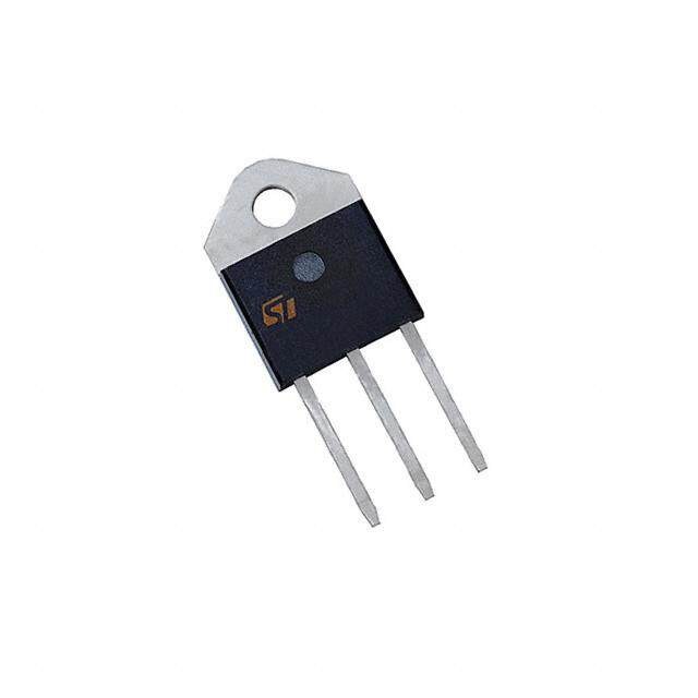
| 描述 | TRIAC ALTERNISTOR 800V 25A TOP3双向可控硅 25 Amp 800 Volt |
| 产品分类 | 双向可控硅分离式半导体 |
| GateTriggerCurrent-Igt | 35 mA |
| GateTriggerVoltage-Vgt | 1.3 V |
| 品牌 | STMicroelectronics |
| 产品手册 | |
| 产品图片 |
|
| rohs | 符合RoHS无铅 / 符合限制有害物质指令(RoHS)规范要求 |
| 产品系列 | 晶体闸流管,双向可控硅,STMicroelectronics BTA26-800CWRGSnubberless™ |
| 数据手册 | |
| 产品型号 | BTA26-800CWRG |
| 三端双向可控硅类型 | 可控硅 - 无缓冲器 |
| 不重复通态电流 | 260 A |
| 产品培训模块 | http://www.digikey.cn/PTM/IndividualPTM.page?site=cn&lang=zhs&ptm=26297http://www.digikey.cn/PTM/IndividualPTM.page?site=cn&lang=zhs&ptm=26298 |
| 产品目录页面 | |
| 产品种类 | 双向可控硅 |
| 供应商器件封装 | TOP3 |
| 保持电流Ih最大值 | 50 mA |
| 关闭状态漏泄电流(在VDRMIDRM下) | 5 uA |
| 其它名称 | 497-4173-5 |
| 其它有关文件 | http://www.st.com/web/catalog/sense_power/FM144/CL1221/SC124/PF76119?referrer=70071840 |
| 包装 | 管件 |
| 商标 | STMicroelectronics |
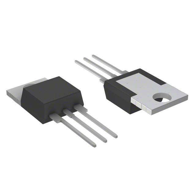
| 安装类型 | 通孔 |
| 安装风格 | Through Hole |
| 封装 | Tube |
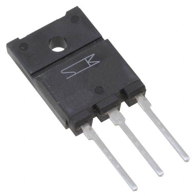
| 封装/外壳 | TOP-3 绝缘 |
| 封装/箱体 | TOP-3 |
| 工厂包装数量 | 30 |
| 开启状态电压 | 1.55 V |
| 最大工作温度 | + 125 C |
| 最大转折电流IBO | 260 A |
| 最小工作温度 | - 40 C |
| 栅极触发电压-Vgt | 1.3 V |
| 栅极触发电流-Igt | 35 mA |
| 标准包装 | 30 |
| 电压-断态 | 800V |
| 电压-栅极触发(Vgt)(最大值) | 1.3V |
| 电流-不重复浪涌50、60Hz(Itsm) | 250A,260A |
| 电流-保持(Ih)(最大值) | 50mA |
| 电流-栅极触发(Igt)(最大值) | 35mA |
| 电流-通态(It(RMS))(最大值) | 25A |
| 系列 | BTA26 |
| 配置 | 单一 |
| 额定重复关闭状态电压VDRM | 800 V |


- 商务部:美国ITC正式对集成电路等产品启动337调查
- 曝三星4nm工艺存在良率问题 高通将骁龙8 Gen1或转产台积电
- 太阳诱电将投资9.5亿元在常州建新厂生产MLCC 预计2023年完工
- 英特尔发布欧洲新工厂建设计划 深化IDM 2.0 战略
- 台积电先进制程称霸业界 有大客户加持明年业绩稳了
- 达到5530亿美元!SIA预计今年全球半导体销售额将创下新高
- 英特尔拟将自动驾驶子公司Mobileye上市 估值或超500亿美元
- 三星加码芯片和SET,合并消费电子和移动部门,撤换高东真等 CEO
- 三星电子宣布重大人事变动 还合并消费电子和移动部门
- 海关总署:前11个月进口集成电路产品价值2.52万亿元 增长14.8%

PDF Datasheet 数据手册内容提取
BTA24, BTB24, BTA25 BTA26, BTB26, T25 25 A standard and Snubberless™ triacs Features A2 ■ High current triac ■ Low thermal resistance with clip bonding G ■ High commutation (4 quadrant) or very high A1 A2 commutation (3 quadrant) capability ■ BTA series UL1557 certified (File ref: 81734) ■ Packages are RoHS (2002/95/EC) compliant A1A2 A1 G A2 G Applications TO-220AB Insulated TO-220AB (BTA24) (BTB24) Applications include the ON/OFF function in A1 applications such as static relays, heating G A2 regulation, induction motor starting circuits, etc., or for phase control operation in light dimmers, motor speed controllers, and silmilar. A1 A2 G The snubberless versions (BTA/BTB...W and T25 RD91 TOP3 Insulated series) are especially recommended for use on (BTA25) (BTA26) inductive loads, due to their high commutation performances. The BTA series provides an A2 insulated tab (rated at 2500 V ). A2 RMS Description A1 A2 G A1 A2 Available either in through-hole or surface-mount G packages, the BTA24, BTB24, BTA25, BTA26, D2PAK TOP3 (T25) (BTB26) BTB26 and T25 triac series is suitable for general purpose mains power AC switching. T able 1. Device summary Symbol Parameter BTA24(1) BTB24 BTA25(1) BTA26(1) BTB26 T25 Unit RMS on-state I 25 25 25 25 25 25 A T(RMS) current Repetitive peak V /V 600 / 800 600 / 800 600 / 800 600(2) / 800 600 600 / 800 V DRM RRM off-state voltage Triggering gate I (Snubberless) 35 / 50 35 / 50 50 35 / 50 - 35 mA GT current Triggering gate I (Standard) - 50 50 50 50 - mA GT current 1. Insulated packages 2. 600 V version available only with I = 50 mA (Snubberless and Standard) GT TM: Snubberless is a trademark of STMicroelectronics July 2007 Rev 10 1/12 www.st.com 12
Characteristics BTA24, BTB24, BTA25, BTA26, BTB26, T25 1 Characteristics Table 2. A bsolute maximum ratings Symbol Parameter Value Unit TOP3 T = 105° C c D2PAK / T = 100° C TO-220AB c I RMS on-state current (full sine wave) 25 A T(RMS) RD91 Ins/ T = 100° C TOP3 Ins. c TO-220AB Ins. T = 75° C c Non repetitive surge peak on-state F = 50 Hz t = 20 ms 250 I A TSM current (full cycle, Tj initial = 25° C) F = 60 Hz t = 16.7 ms 260 I²t I²t Value for fusing t = 10 ms 340 A²s p Critical rate of rise of on-state current dI/dt F = 120 Hz T = 125° C 50 A/µs I = 2 x I , t ≤ 100 ns j G GT r Non repetitive surge peak off-state V /V V /V t = 10 ms T = 25° C DRM RRM V DSM RSM voltage p j + 100 I Peak gate current t = 20 µs T = 125° C 4 A GM p j P Average gate power dissipation T = 125° C 1 W G(AV) j T Storage junction temperature range - 40 to + 150 stg ° C T Operating junction temperature range - 40 to + 125 j Table 3. E lectrical characteristics (T = 25° C, unless otherwise specified), Snubberless and j logic level (3 quadrants) T25, BTA/BTB24...W, BTA25...W, BTA26...W T25 BTA/BTB Symbol Test Conditions Quadrant Unit T2535 CW BW I (1) I - II - III MAX. 35 35 50 mA GT V = 12 V R = 33 Ω D L V I - II - III MAX. 1.3 V GT V = V R = 3.3 kΩ V D DRM L I - II - III MIN. 0.2 V GD T = 125° C j I (2) I = 500 mA MAX. 50 50 75 mA H T I - III 70 70 80 I I = 1.2 I MAX. mA L G GT II 80 80 100 dV/dt(2) V = 67 %V gate open T = 125° C MIN. 500 500 1000 V/µs D DRM j (dI/dt)c(2) Without snubber T = 125° C MIN. 13 13 22 A/ms j 1. minimum I is guaranted at 5% of I max. GT GT 2. for both polarities of A2 referenced to A1. 2/12
BTA24, BTB24, BTA25, BTA26, BTB26, T25 Characteristics Table 4. E lectrical characteristics (T = 25° C, unless otherwise specified), j standard (4 quadrants), BTB24...B, BTA25...B, BTA26...B, BTB26...B Symbol Test Conditions Quadrant Value Unit I - II - III 50 I (1) MAX. mA GT V = 12 V R = 33 Ω IV 100 D L V ALL MAX. 1.3 V GT V V = V R = 3.3 kΩ T = 125° C ALL MIN. 0.2 V GD D DRM L j I (2)) I = 500 mA MAX. 80 mA H T I - III - IV 70 I I = 1.2 I MAX. mA L G GT II 160 dV/dt(2) V = 67 %V gate open T = 125° C MIN. 500 V/µs D DRM j (dV/dt)c(2) (dI/dt)c = 13.3 A/ms T = 125° C MIN. 10 V/µs j 1. minimum I is guaranted at 5% of I max. GT GT 2. for both polarities of A2 referenced to A1. Table 5. S tatic characteristics Symbol Test Conditions Value Unit V (1) I = 35 A t = 380 µs T = 25° C MAX. 1.55 V TM TM p j V (1) Threshold voltage T = 125° C MAX. 0.85 V t0 j R (1) Dynamic resistance T = 125° C MAX. 16 mΩ d j IDRM V = V Tj = 25° C MAX. 5 µA IRRM DRM RRM Tj = 125° C 3 mA 1. for both polarities of A2 referenced to A1. Table 6. T hermal resistance Symbol Parameter Value Unit TOP 3 0.6 D2PAK / TO-220AB 0.8 R Junction to case (AC) ° C/W th(j-c) RD91 Insulated / TOP3 Insulated 0.9 TO-220AB Insulated 1.7 (1)S = 1 cm² D2PAK 45 R Junction to ambient TOP3 / TOP3 Insulated 50 ° C/W th(j-a) TO-220AB / TO-220AB Insulated 60 1. S = Copper surface under tab. 3/12
Characteristics BTA24, BTB24, BTA25, BTA26, BTB26, T25 Figure 1. M aximum power dissipation versus Figure 2. RMS on-state current versus case RMS on-state current (full cycle) temperature (full cycle) P(W) IT(RMS)(A) 30 30 BTB26 25 25 BTA24 20 20 15 15 BTB24 /T25xx / BTA25 / BTA26 10 10 5 5 IT(RMS)(A) TC(°C) 0 0 0 5 10 15 20 25 0 25 50 75 100 125 Figure 3. D 2PAK RMS on-state current versus Figure 4. Relative variation of thermal ambient temperature (printed impedance versus pulse circuit board FR4, copper duration thickness: 35µm) (full cycle) IT(RMS)(A) K=[Zth/Rth] 4.0 1E+0 3.5 (SD=21PcAmK2) Zth(j-c) 3.0 1E-1 Zth(j-a) 2.5 BTA / BTB24 /T25 2.0 1.5 1E-2 Zth(j-a) BTA26 1.0 0.5 Tamb(°C) tp(s) 0.0 1E-3 0 25 50 75 100 125 1E-3 1E-2 1E-1 1E+0 1E+1 1E+2 5E+2 Figure 5. O n-state characteristics Figure 6. Surge peak on-state current (maximum values) versus number of cycles ITM(A) ITSM(A) 300 300 Tjmax. 100 RVdto== 106.8 m5VΩ Tj=Tjmax. 250 t=20ms 200 One cycle Non repetitive Tjinitial=25°C 150 10 Tj= 25°C. 100 RTeCp=e7t5it°ivCe 50 VTM(V) Number of cycles 1 0 0.5 1.0 1.5 2.0 2.5 3.0 3.5 4.0 4.5 1 10 100 1000 4/12
BTA24, BTB24, BTA25, BTA26, BTB26, T25 Characteristics Figure 7. N on-repetitive surge peak on-state Figure 8. Relative variation of gate trigger current for a sinusoidal pulse with current, holding current and width t < 10 ms and corresponding latching current versus junction p value of I2t temperature (typical values) ITSM(A),I 2t (A 2s) IGT,IH,IL[Tj] /IGT,IH,IL[Tj=25°C] 3000 2.5 dI/dt limitation: Tjinitial=25°C 50A/µs 2.0 1000 IGT ITSM 1.5 I 2t 1.0 IH& IL 0.5 tp(ms) Tj(°C) 100 0.0 0.01 0.10 1.00 10.00 -40 -20 0 20 40 60 80 100 120 140 Figure 9. R elative variation of critical rate of Figure 10. Relative variation of critical rate of decrease of main current versus decrease of main current versus T j (dV/dt)c (typical values) (dI/dt)c [(dV/dt)c] / Specified (dI/dt)c (dI/dt)c [Tj] /(dI/dt)c [Tjspecified] 2.4 6 2.2 5 2.0 1.8 4 1.6 1.4 B T2535/CW/BW 3 1.2 1.0 2 0.8 1 0.6 (dV/dt)c (V/µs) Tj(°C) 0.4 0 0.1 1.0 10.0 100.0 0 25 50 75 100 125 F igure 11. D2PAK thermal resistance junction to ambient versus copper surface under tab (printed circuit board FR4, copper thickness: 35µm) Rth(j-a)(°C/W) 80 70 D2PAK 60 50 40 30 20 10 S(cm²) 0 0 4 8 12 16 20 24 28 32 36 40 5/12
Ordering information scheme BTA24, BTB24, BTA25, BTA26, BTB26, T25 2 Ordering information scheme Figure 12. BTA and BTB series BT A 24 - 600 BW RG Triac series Insulation A = insulated B = non insulated Current 24 = 25 A inTO-220AB 25 = 25 A in RD91 26 = 25 A inTOP3 Voltage 600 = 600V 800 = 800V Sensitivity and type B = 50 mA Standard BW = 50 mA Snubberless CW = 35 mASnubberless Packing mode RG =Tube Figure 13. T25 series T 25 35 - 600 G (-TR) Triac series Current 25 = 25 A Sensitivity 35 = 35 mA Voltage 600 = 600V 800 = 800V Package G = D 2PAK Packing mode Blank =Tube -TR =Tape and Reel 6/12
BTA24, BTB24, BTA25, BTA26, BTB26, T25 Package information 3 Package information ● Epoxy meets UL94,V0 ● Cooling method: C ● Recommended torque value: 0.4 - 0.5 Nm (TO-220AB), 0.9 - 1.2 Nm (TOP3 and RD91) ● Maximum torque value for BTB24 is 0.5 Nm T able 7. D2PAK dimensions DIMENSIONS REF. Millimeters Inches Min. Typ. Max. Min. Typ. Max. A 4.30 4.60 0.169 0.181 A E A1 2.49 2.69 0.098 0.106 C2 L2 A2 0.03 0.23 0.001 0.009 B 0.70 0.93 0.027 0.037 D L B2 1.25 1.40 0.048 0.055 L3 C 0.45 0.60 0.017 0.024 A1 B2 C2 1.21 1.36 0.047 0.054 C R B D 8.95 9.35 0.352 0.368 G E 10.00 10.28 0.393 0.405 A2 G 4.88 5.28 0.192 0.208 2mm min. FLAT ZONE L 15.00 15.85 0.590 0.624 V2 L2 1.27 1.40 0.050 0.055 L3 1.40 1.75 0.055 0.069 R 0.40 0.016 V2 0° 8° 0° 8° Figure 14. D2PAK footprint dimensions (in millimeters) 16.90 10.30 5.08 1.30 3.70 8.90 7/12
Package information BTA24, BTB24, BTA25, BTA26, BTB26, T25 T able 8. RD91 dimensions DIMENSIONS REF. Millimeters Inches Min. Max. Min. Max. A 40.00 1.575 A2 L2 L1 A1 29.90 30.30 1.177 1.193 A2 22.00 0.867 B2 B 27.00 1.063 C B1 B1 13.50 16.50 0.531 0.650 B2 24.00 0.945 C2 A1 C1 C 14.00 0.551 C1 3.50 0.138 N2 N1 C2 1.95 3.00 0.077 0.118 B F E3 0.70 0.90 0.027 0.035 E3 F 4.00 4.50 0.157 0.177 I A I 11.20 13.60 0.441 0.535 L1 3.10 3.50 0.122 0.138 L2 1.70 1.90 0.067 0.075 N1 33° 43° 33° 43° N2 28° 38° 28° 38° 8/12
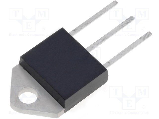
BTA24, BTB24, BTA25, BTA26, BTB26, T25 Package information T able 9. TOP3 (insulated and non_insulated) dimensions DIMENSIONS REF. Millimeters Inches Min. Typ. Max. Min. Typ. Max. H A A 4.4 4.6 0.173 0.181 R ØL B B 1.45 1.55 0.057 0.061 C 14.35 15.60 0.565 0.614 K D 0.5 0.7 0.020 0.028 F G E 2.7 2.9 0.106 0.114 F 15.8 16.5 0.622 0.650 G 20.4 21.1 0.815 0.831 P C H 15.1 15.5 0.594 0.610 J 5.4 5.65 0.213 0.222 D J J E K 3.4 3.65 0.134 0.144 ØL 4.08 4.17 0.161 0.164 P 1.20 1.40 0.047 0.055 R 4.60 0.181 9/12
Package information BTA24, BTB24, BTA25, BTA26, BTB26, T25 T able 10. TO-220AB (insulated and non-insulated) dimensions DIMENSIONS REF. Millimeters Inches Min. Typ. Max. Min. Typ. Max. A 15.20 15.90 0.598 0.625 a1 3.75 0.147 B C a2 13.00 14.00 0.511 0.551 Ø I b2 B 10.00 10.40 0.393 0.409 L F b1 0.61 0.88 0.024 0.034 A b2 1.23 1.32 0.048 0.051 I4 C 4.40 4.60 0.173 0.181 l3 a1 c2 c1 0.49 0.70 0.019 0.027 l2 c2 2.40 2.72 0.094 0.107 a2 e 2.40 2.70 0.094 0.106 M b1 c1 F 6.20 6.60 0.244 0.259 e ØI 3.75 3.85 0.147 0.151 I4 15.80 16.40 16.80 0.622 0.646 0.661 L 2.65 2.95 0.104 0.116 l2 1.14 1.70 0.044 0.066 l3 1.14 1.70 0.044 0.066 M 2.60 0.102 In order to meet environmental requirements, ST offers these devices in ECOPACK® packages. These packages have a lead-free second level interconnect. The category of second level interconnect is marked on the package and on the inner box label, in compliance with JEDEC Standard JESD97. The maximum ratings related to soldering conditions are also marked on the inner box label. ECOPACK is an ST trademark. ECOPACK specifications are available at: www.st.com. 10/12
BTA24, BTB24, BTA25, BTA26, BTB26, T25 Ordering information 4 Ordering information T able 11. Ordering information Ordering type Marking Package Weight Base qty Delivery mode BTA/BTB24-xxxyzRG BTA/BTB24 xxxyz TO-220AB 2.3 g 50 Tube BTA25-xxxyz BTA25xxxyz RD91 20 g 25 Bulk BTA26-xxxyRG BTA26xxxyz TOP3 Ins. 4.5 g 30 Tube BTB26-600BRG BTB26600B TOP3 4.5 g 30 Tube T2535-xxxG T2535 xxxG 50 Tube D2PAK 1.5 g T2535-xxxG-TR T2535 xxxG 1000 Tape and reel Note: xxx = voltage, y = sensitivity, z = type 5 Revision history T able 12. Revision history Date Revision Description of changes Oct-2002 6A Previous update. TO-220AB delivery mode changed from bulk to tube. 13-Feb-2006 7 ECOPACK statement added. 31-May-2006 8 Reformatted to current standard. T in figure 3 changed to T c amb 31-Jul-2006 9 Typing error corrected on page 1 (BTB124 instead of BTB24) Added BTB26-600BRG. Restructured cover page and section 2: Ordering information scheme on page6 to simplify product selection. 05-Jul-2007 10 Thermal resistance values updated in Table6 and Figure2. Graphic for I2t updated in Figure7. 11/12
BTA24, BTB24, BTA25, BTA26, BTB26, T25 Please Read Carefully: Information in this document is provided solely in connection with ST products. STMicroelectronics NV and its subsidiaries (“ST”) reserve the right to make changes, corrections, modifications or improvements, to this document, and the products and services described herein at any time, without notice. All ST products are sold pursuant to ST’s terms and conditions of sale. Purchasers are solely responsible for the choice, selection and use of the ST products and services described herein, and ST assumes no liability whatsoever relating to the choice, selection or use of the ST products and services described herein. No license, express or implied, by estoppel or otherwise, to any intellectual property rights is granted under this document. If any part of this document refers to any third party products or services it shall not be deemed a license grant by ST for the use of such third party products or services, or any intellectual property contained therein or considered as a warranty covering the use in any manner whatsoever of such third party products or services or any intellectual property contained therein. UNLESS OTHERWISE SET FORTH IN ST’S TERMS AND CONDITIONS OF SALE ST DISCLAIMS ANY EXPRESS OR IMPLIED WARRANTY WITH RESPECT TO THE USE AND/OR SALE OF ST PRODUCTS INCLUDING WITHOUT LIMITATION IMPLIED WARRANTIES OF MERCHANTABILITY, FITNESS FOR A PARTICULAR PURPOSE (AND THEIR EQUIVALENTS UNDER THE LAWS OF ANY JURISDICTION), OR INFRINGEMENT OF ANY PATENT, COPYRIGHT OR OTHER INTELLECTUAL PROPERTY RIGHT. UNLESS EXPRESSLY APPROVED IN WRITING BY AN AUTHORIZED ST REPRESENTATIVE, ST PRODUCTS ARE NOT RECOMMENDED, AUTHORIZED OR WARRANTED FOR USE IN MILITARY, AIR CRAFT, SPACE, LIFE SAVING, OR LIFE SUSTAINING APPLICATIONS, NOR IN PRODUCTS OR SYSTEMS WHERE FAILURE OR MALFUNCTION MAY RESULT IN PERSONAL INJURY, DEATH, OR SEVERE PROPERTY OR ENVIRONMENTAL DAMAGE. ST PRODUCTS WHICH ARE NOT SPECIFIED AS "AUTOMOTIVE GRADE" MAY ONLY BE USED IN AUTOMOTIVE APPLICATIONS AT USER’S OWN RISK. Resale of ST products with provisions different from the statements and/or technical features set forth in this document shall immediately void any warranty granted by ST for the ST product or service described herein and shall not create or extend in any manner whatsoever, any liability of ST. ST and the ST logo are trademarks or registered trademarks of ST in various countries. Information in this document supersedes and replaces all information previously supplied. The ST logo is a registered trademark of STMicroelectronics. All other names are the property of their respective owners. © 2007 STMicroelectronics - All rights reserved STMicroelectronics group of companies Australia - Belgium - Brazil - Canada - China - Czech Republic - Finland - France - Germany - Hong Kong - India - Israel - Italy - Japan - Malaysia - Malta - Morocco - Singapore - Spain - Sweden - Switzerland - United Kingdom - United States of America www.st.com 12/12
Mouser Electronics Authorized Distributor Click to View Pricing, Inventory, Delivery & Lifecycle Information: S TMicroelectronics: BTA25-600BW BTA25-800BW BTA25-600B BTB24-600BRG BTA26-600BRG BTA26-400BRG BTB24-800CWRG T2535-600G-TR BTA26-800BWRG BTA24-800BWRG BTA24-800CWRG BTA26-800CWRG BTB24-600BWRG BTB24-600CWRG BTA25-700B BTA25-800B BTB26-600BRG T2535-600G BTA24-600BWRG BTA26-600BWRG BTA24-600CWRG BTB24-800BWRG BTA26-800BRG BTB24-800BRG BTA26-700BRG T2535-800G-TR T2535- 800G