ICGOO在线商城 > 隔离器 > 光隔离器 - 逻辑输出 > PS9117A-F3-AX
 Datasheet下载
- 型号: PS9117A-F3-AX
- 制造商: CEL
- 库位|库存: xxxx|xxxx
- 要求:
| 数量阶梯 | 香港交货 | 国内含税 |
| +xxxx | $xxxx | ¥xxxx |
查看当月历史价格
查看今年历史价格
PS9117A-F3-AX产品简介:
ICGOO电子元器件商城为您提供PS9117A-F3-AX由CEL设计生产,在icgoo商城现货销售,并且可以通过原厂、代理商等渠道进行代购。 PS9117A-F3-AX价格参考。CELPS9117A-F3-AX封装/规格:光隔离器 - 逻辑输出, Logic Output Optoisolator 10Mbps Open Collector 3750Vrms 1 Channel 15kV/µs CMTI 5-SO。您可以下载PS9117A-F3-AX参考资料、Datasheet数据手册功能说明书,资料中有PS9117A-F3-AX 详细功能的应用电路图电压和使用方法及教程。
CEL品牌的PS9117A-F3-AX光隔离器是一款逻辑输出型的光电隔离器件,广泛应用于需要电气隔离和信号传输的场景中。其主要应用场景包括:

 1. 工业自动化控制系统
在工业自动化领域,设备之间的信号传输往往需要电气隔离以防止干扰和损坏。PS9117A-F3-AX可以用于PLC(可编程逻辑控制器)、传感器、执行器等设备之间的信号隔离与传输,确保信号的稳定性和安全性。特别是在高压、强电磁干扰环境下,该光隔离器能够有效隔离输入和输出端的电压,避免电流回路对系统的影响。

 2. 电力监控系统
电力监控系统中,变电站、配电柜等设备之间需要进行信号传输,但这些设备通常处于不同的电位环境中。使用PS9117A-F3-AX可以实现高低压侧的电气隔离,防止高压侧的瞬态电压对低压侧控制电路造成损害,同时保证信号的准确传递。它还可以用于电力线通信、智能电表等场合,确保数据传输的安全性和可靠性。

 3. 医疗设备
在医疗设备中,患者安全是首要考虑的因素。PS9117A-F3-AX可用于心电图机、监护仪、呼吸机等设备中的信号隔离,防止外界干扰或电源波动对患者的健康产生影响。通过光隔离技术,它可以将敏感的生物电信号与外部电路隔离开来,确保信号的纯净度和稳定性。

 4. 通信设备
在通信领域,特别是有线通信和光纤通信中,信号传输的距离较长且环境复杂。PS9117A-F3-AX可以用于调制解调器、路由器、交换机等设备中的信号隔离,确保数据传输的稳定性和抗干扰能力。它还适用于RS-485、CAN总线等通信接口,提供可靠的电气隔离。

 5. 汽车电子
现代汽车中越来越多地采用电子控制系统,如发动机控制单元(ECU)、车身控制模块(BCM)等。PS9117A-F3-AX可以在这些模块中用于信号隔离,防止电磁干扰和电压波动对系统的影响,确保汽车电子系统的正常运行。

总之,PS9117A-F3-AX光隔离器凭借其高可靠性和电气隔离特性,在多个行业中有着广泛的应用,尤其是在需要电气隔离和信号传输的场景下表现尤为出色。
| 参数 | 数值 |
| 产品目录 | |
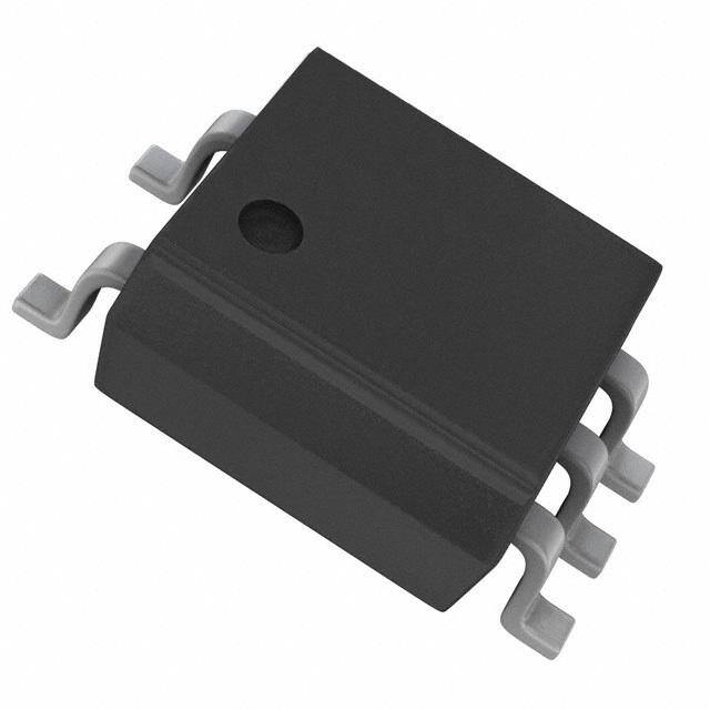
| 描述 | PHOTOCOUPLER OPEN HS OUT 5-SOP |
| 产品分类 | |
| 品牌 | CEL |
| 数据手册 | |
| 产品图片 |
|
| 产品型号 | PS9117A-F3-AX |
| rohs | 无铅 / 符合限制有害物质指令(RoHS)规范要求 |
| 产品系列 | NEPOC |
| 上升/下降时间(典型值) | 20ns, 5ns |
| 产品培训模块 | http://www.digikey.cn/PTM/IndividualPTM.page?site=cn&lang=zhs&ptm=22067 |
| 产品目录页面 | |
| 传播延迟tpLH/tpHL(最大值) | 75ns, 75ns |
| 供应商器件封装 | 5-SO |
| 共模瞬态抗扰度(最小值) | 15kV/µs |
| 其它名称 | PS9117A-F3-AXDKR |
| 其它图纸 |
|
| 包装 | Digi-Reel® |
| 安装类型 | 表面贴装 |
| 封装/外壳 | 6-SOIC(0.173",4.40mm 宽,5 引线) |
| 工作温度 | -40°C ~ 85°C |
| 数据速率 | 10Mbps |
| 标准包装 | 1 |
| 电压-正向(Vf)(典型值) | 1.65V |
| 电压-电源 | 4.5 V ~ 5.5 V |
| 电压-隔离 | 3750Vrms |
| 电流-DC正向(If) | 30mA |
| 电流-输出/通道 | 25mA |
| 输入-输入侧1/输入侧2 | 1/0 |
| 输入类型 | DC |
| 输出类型 | 开路集电极 |
| 通道数 | 1 |


- 商务部:美国ITC正式对集成电路等产品启动337调查
- 曝三星4nm工艺存在良率问题 高通将骁龙8 Gen1或转产台积电
- 太阳诱电将投资9.5亿元在常州建新厂生产MLCC 预计2023年完工
- 英特尔发布欧洲新工厂建设计划 深化IDM 2.0 战略
- 台积电先进制程称霸业界 有大客户加持明年业绩稳了
- 达到5530亿美元!SIA预计今年全球半导体销售额将创下新高
- 英特尔拟将自动驾驶子公司Mobileye上市 估值或超500亿美元
- 三星加码芯片和SET,合并消费电子和移动部门,撤换高东真等 CEO
- 三星电子宣布重大人事变动 还合并消费电子和移动部门
- 海关总署:前11个月进口集成电路产品价值2.52万亿元 增长14.8%
.jpg)


PDF Datasheet 数据手册内容提取
PHOTOCOUPLER PS9117A HIGH CMR, 10 Mbps OPEN COLLECTOR OUTPUT TYPE 5-PIN SOP (SO-5) HIGH-SPEED PHOTOCOUPLER −NEPOC Series− DESCRIPTION The PS9117A is an optically coupled high-speed, active low type isolator containing a GaAlAs LED on the input side and a photodiode and a signal processing circuit on the output side on one chip. The PS9117A is designed specifically for high common mode transient immunity (CMR) and low pulse width distortion. The PS9117A is suitable for high density application. FEATURES • Pulse width distortion (⏐tPHL − tPLH⏐ = 35 ns MAX.) • High common mode transient immunity (CMH, CML = ±15 kV/μs MIN.) PIN CONNECTION • Small package (SO-5) (Top View) • High-speed (10 Mbps) 5 4 3 • High isolation voltage (BV = 3 750 Vr.m.s.) • Open collector output 1.Anode 2.Cathode • Ordering number of taping product: PS9117A-F3: 2 500 pcs/reel 3.GND • Pb-Free product 4.VO 5.VCC • Safety standards • UL approved: File No. E72422 1 2 • DIN EN60747-5-2 (VDE0884 Part2) approved No. 40008902 (Option) • CSA approved: File No. 2115283 (CA 101391) TRUTH TABLE APPLICATIONS LED Output • Measurement equipment • PDP ON L • FA Network OFF H Document No. PN10646EJ04V0DS (4th edition) Date Published July 2008 NS The mark <R> shows major revised points. The revised points can be easily searched by copying an "<R>" in the PDF file and specifying it in the "Find what:" field.
PS9117A PACKAGE DIMENSIONS (UNIT: mm) 3.4+0.3 –0.1 5 4 3 7.0±0.3 4.4 1 2 0.2 +0.105–0.05 ± 1 2.6 0. 1 1.27 0.5±0.3 0. ± 0.1 0.4+–00..0150 0.25 M <R> MARKING EXAMPLE SnBi PLATING Ni/Pd/Au PLATING 117A Type Number 117A Type Number N831 Assembly Lot N831 Assembly Lot *1 No. 1 pin Mark *1 No. 1 pin Mark N 8 31 N 8 31 Week Assembled Week Assembled Year Assembled Year Assembled (Last 1 Digit) (Last 1 Digit) Rank Code Rank Code *1 Bar : Pb-Free *1 Bar : Pb-Free 2 Data Sheet PN10646EJ04V0DS
PS9117A <R> ORDERING INFORMATION Part Number Order Number Solder Plating Packing Style Safety Standards Application Specification Approval Part Number*1 PS9117A PS9117A-A Pb-Free 20 pcs (Tape 20 pcs cut) Standard products PS9117A PS9117A-F3 PS9117A-F3-A (SnBi) Embossed Tape 2 500 pcs/reel (UL approved) PS9117A-V PS9117A-V-A 20 pcs (Tape 20 pcs cut) DIN EN60747-5-2 PS9117A-V-F3 PS9117A-V-F3-A Embossed Tape 2 500 pcs/reel (VDE0884 Part2) approved (Option) PS9117A PS9117A-AX Pb-Free 20 pcs (Tape 20 pcs cut) Standard products PS9117A-F3 PS9117A-F3-AX (Ni/Pd/Au) Embossed Tape 2 500 pcs/reel (UL approved) PS9117A-V PS9117A-V-AX 20 pcs (Tape 20 pcs cut) DIN EN60747-5-2 PS9117A-V-F3 PS9117A-V-F3-AX Embossed Tape 2 500 pcs/reel (VDE0884 Part2) approved (Option) *1 For the application of the Safety Standard, following part number should be used. ABSOLUTE MAXIMUM RATINGS (TA = 25°C, unless otherwise specified) Parameter Symbol Ratings Unit Diode Forward Current*1 IF 30 mA Reverse Voltage VR 5 V Detector Supply Voltage VCC 7 V Output Voltage VO 7 V Output Current IO 25 mA Power Dissipation*2 PC 40 mW Isolation Voltage*3 BV 3750 Vr.m.s. Operating Ambient Temperature TA −40 to +85 °C Storage Temperature Tstg −55 to +125 °C *1 Reduced to 0.3 mA/°C at TA = 25°C or more. *2 Applies to output pin VO (collector pin). Reduced to 1.5 mW/°C at TA = 65°C or more. *3 AC voltage for 1 minute at TA = 25°C, RH = 60% between input and output. Pins 1-2 shorted together, 3-5 shorted together. RECOMMENDED OPERATING CONDITIONS Parameter Symbol MIN. TYP. MAX. Unit Low Level Input Voltage VFL 0 0.8 V High Level Input Current IFH 6.3 10 12.5 mA Supply Voltage VCC 4.5 5.0 5.5 V TTL (RL = 1 kΩ, loads) N 5 Pull-up Resistor RL 330 4 k Ω Data Sheet PN10646EJ04V0DS 3
PS9117A ELECTRICAL CHARACTERISTICS (TA = −40 to +85°C, unless otherwise specified) Parameter Symbol Conditions MIN. TYP.*1 MAX. Unit Diode Forward Voltage VF I F = 10 mA, TA = 25°C 1.4 1.65 1.8 V Reverse Current IR V R = 3 V, TA = 25°C 10 μA Terminal Capacitance Ct V = 0 V, f = 1 MHz, TA = 25°C 30 pF Detector High Level Output Current IOH V CC = VO = 5.5 V, VF = 0.8 V 1 100 μA <R> Low Level Output Voltage*2 V OL V CC = 5.5 V, IF = 5 mA, IOL = 13 mA 0.2 0.6 V High Level Supply Current ICCH V CC = 5.5 V, IF = 0 mA, VO = open 4 7 mA Low Level Supply Current ICCL V CC = 5.5 V, IF = 10 mA, VO = open 6 10 Coupled Threshold Input Current IFHL V CC = 5 V, VO = 0.8 V, RL = 350 Ω 2 5 (H → L) Isolation Resistance RI-O V I-O = 1 kVDC, RH = 40 to 60%, 1011 Ω TA = 25°C Isolation Capacitance CI-O V = 0 V, f = 1 MHz, TA = 25°C 0.6 pF Propagation Delay Time tPHL TA = 25°C 40 75 ns (H → L)*3 100 Propagation Delay Time tPLH TA = 25°C 45 75 (L → H)*3 100 Rise Time tr V CC = 5 V, RL = 350 Ω, IF = 7.5 mA, 20 Fall Time tf V THHL = VTHLH = 1.5 V 5 Pulse Width Distortion ⏐tPHL-tPLH⏐ 5 35 (PWD)*3 Propagation Delay Skew tPSK 40 Common Mode CMH V CC = 5 V, RL = 350 Ω, TA = 25°C, 15 20 kV/μs Transient Immunity at High IF = 0 mA, VO > 2 V, VCM = 1 kV Level Output*4 Common Mode CML V CC = 5 V, RL = 350 Ω, TA = 25°C, 15 20 kV/μs Transient Immunity at Low IF = 7.5 mA, VO < 0.8 V, VCM = 1 kV Level Output*4 4 Data Sheet PN10646EJ04V0DS
PS9117A *1 Typical values at TA = 25°C *2 Because VOL of 2 V or more may be output when LED current input and when output supply of VCC = 2.6 V or less, it is important to confirm the characteristics (operation with the power supply on and off) during design, before using this device. *3 Test circuit for propagation delay time Input (IF = 7.5 mA) Pulse input (IF) VCC = 5 V 50% (PW = 1 μ s, 0.1 μ F RL = 350 Ω Duty cycle = 1/10) VO (monitor) Input CL = 15 pF Output (monitor) 1.5 V 47 Ω VOL tPHL tPLH Remark CL includes probe and stray wiring capacitance. *4 Test circuit for common mode transient immunity 1 kV VCM 90% SW IF VCC = 5 V 0.1 μ F RL = 350 Ω 10% 0 V CL = 15 pFVO (monitor) tr tf VO VOH (IF = 0 mA) 2 V VCM 0.8 V VO VOL (IF = 7.5 mA) Remark CL includes probe and stray wiring capacitance. USAGE CAUTIONS 1. This product is weak for static electricity by designed with high-speed integrated circuit so protect against static electricity when handling. 2. By-pass capacitor of 0.1 μF is used between VCC and GND near device. Also, ensure that the distance between the leads of the photocoupler and capacitor is no more than 10 mm. 3. Avoid storage at a high temperature and high humidity. Data Sheet PN10646EJ04V0DS 5
PS9117A TYPICAL CHARACTERISTICS (TA = 25°C, unless otherwise specified) MAXIMUM FORWARD CURRENT DETECTOR POWER DISSIPATION vs. AMBIENT TEMPERATURE vs. AMBIENT TEMPERATURE 40 50 A) W) m m nt I (F 30 n P (C 40 e o urr ati 30 C p d 20 ssi ar Di Forw wer 20 m Po mu 10 or 10 Maxi etect D 0 20 40 60 8085 100 0 20 40 60 8085 100 Ambient Temperature TA (˚C) Ambient Temperature TA (˚C) FORWARD CURRENT vs. SUPPLY CURRENT vs. FORWARD VOLTAGE AMBIENT TEMPERATURE 100 12 ard Current I (mA)F 110 TA = +++–522805055˚˚˚˚˚CCCCC Supply Current I (mA)CCHSupply Current I (mA)CCL 10864 IICCCCLH ((IIFF == 100 m mAA)) Forw 0.1 gh Level w Level 2 HiLo 0.01 0 1.0 1.2 1.4 1.6 1.8 2.0 2.2 2.4 –50 –25 0 25 50 75 100 Forward Voltage VF (V) Ambient Temperature TA (˚C) OUTPUT VOLTAGE vs. LOW LEVEL OUTPUT VOLTAGE vs. FORWARD CURRENT AMBIENT TEMPERATURE 6 0.6 IF = 5.0 mA, VCC = 5.0 V V) VCC = 5.5 V 5 (OL 0.5 V (V)O 4 RL =1 3.05 0k ΩΩ age V 0.4 e olt oltag 3 4.0 kΩ, 4.7 kΩ put V 0.3 IOL = 1136..00 mmAA Output V 2 evel Out 0.2 106..00 mmAA L 1 w 0.1 o L 0 0 1 2 3 4 5 6 –50 –25 0 25 50 75 100 Forward Current IF (mA) Ambient Temperature TA (˚C) Remark The graphs indicate nominal characteristics. 6 Data Sheet PN10646EJ04V0DS
PS9117A THRESHOLD INPUT CURRENT vs. PROPAGATION DELAY TIME vs. AMBIENT TEMPERATURE AMBIENT TEMPERATURE 5 100 mA) VVCOC = = 0 5.6.0 V V, (ns)H VIF C=C 7=. 55 .m0 AV, ent I (FHL 43 RL = 350 Ω e t, tPHLPL 8600 tPLH: RL = 4.7 kΩ put Curr 2 1.0 kΩ elay Tim 40 tPLH: RL = 1.0 kΩ tPLH: RL = 4.0 kΩ n D hreshold I 1 4.0 kΩ pagation 20 tPHL: RL = 350 Ω, 1.0 tkPLΩH:, R4.L0 = k 3Ω5, 04 .Ω7 kΩ T o Pr 0 0 –50 –25 0 25 50 75 100 –50 –25 0 25 50 75 100 Ambient Temperature TA (˚C) Ambient Temperature TA (˚C) PULSE WIDTH DISTORTION vs. PROPAGATION DELAY TIME vs. AMBIENT TEMPERATURE FORWARD CURRENT 60 100 s) IF = 7.5 mA, s) –t (nHLPLH 5400 VCC = 5.0 V RL = 4.7 kΩ , t (nPHLPLH 80 VCC = 5.0 V tPLH: RL = 4.7 kΩ h Distortion tP 3200 RL = 4.0 kΩ n Delay Time t 4600 tPLH: RL = 1.0 kΩ tPLH: tRPLLH =: R 4L. 0= k3Ω50 Ω Widt RL = 1.0 kΩ atio 20 se 10 pag tPHL: RL = 350 Ω, 1.0 kΩ, 4.0 kΩ, 4.7 kΩ Pul 0 RL = 350 Ω Pro 0 –50 –25 0 25 50 75 100 5 7 9 11 13 15 Ambient Temperature TA (˚C) Forward Current IF (mA) Remark The graphs indicate nominal characteristics. Data Sheet PN10646EJ04V0DS 7
PS9117A TAPING SPECIFICATIONS (UNIT: mm) Outline and Dimensions (Tape) 1 0. 2.0±0.05 ± 4.0±0.1 1.5+–00. 1 1.75 ±0.1 3.45 MAX. 4 7. 1 2 0. 0. ± ± 5 0 5. 2. 1 1.55±0.1 3.9±0.1 3.0±0.1 8.0±0.1 0.3±0.05 Tape Direction PS9117A-F3 Outline and Dimensions (Reel) 2.0±0.5 2.0±0.5 13.0±0.2 0 0 2 2. 1. 0. ± ± ± 0 0 0 R 1.0 21.0±0.8 φ33 φ10 φ13. 13.5±1.0 17.5±1.0 11.9 to 15.4 Outer edge of Packing: 2 500 pcs/reel flange 8 Data Sheet PN10646EJ04V0DS
PS9117A <R> RECOMMENDED MOUNT PAD DIMENSIONS (UNIT: mm) 1.45 8 0. 7 2 1. 5.5 Data Sheet PN10646EJ04V0DS 9
PS9117A NOTES ON HANDLING 1.Recommended soldering conditions (1)Infrared reflow soldering • Peak reflow temperature 260°C or below (package surface temperature) • Time of peak reflow temperature 10 seconds or less • Time of temperature higher than 220°C 60 seconds or less • Time to preheat temperature from 120 to 180°C 120±30 s • Number of reflows Three • Flux Rosin flux containing small amount of chlorine (The flux with a maximum chlorine content of 0.2 Wt% is recommended.) Recommended Temperature Profile of Infrared Reflow C) T (˚ (htoe a1t0in sg) e ur 260˚C MAX. erat 220˚C p m to 60 s e T e c 180˚C a urf S 120˚C ge 120±30 s ka (preheating) c a P Time (s) (2)Wave soldering • Temperature 260°C or below (molten solder temperature) • Time 10 seconds or less • Preheating conditions 120°C or below (package surface temperature) • Number of times One (Allowed to be dipped in solder including plastic mold portion.) • Flux Rosin flux containing small amount of chlorine (The flux with a maximum chlorine content of 0.2 Wt% is recommended.) (3)Soldering by Soldering Iron • Peak Temperature (lead part temperature) 350°C or below • Time (each pins) 3 seconds or less • Flux Rosin flux containing small amount of chlorine (The flux with a maximum chlorine content of 0.2 Wt% is recommended.) (a)Soldering of leads should be made at the point 1.5 to 2.0 mm from the root of the lead (b)Please be sure that the temperature of the package would not be heated over 100°C 10 Data Sheet PN10646EJ04V0DS
PS9117A (4)Cautions • Fluxes Avoid removing the residual flux with freon-based and chlorine-based cleaning solvent. 2.Cautions regarding noise Be aware that when voltage is applied suddenly between the photocoupler’s input and output or between collector-emitters at startup, the output transistor may enter the on state, even if the voltage is within the absolute maximum ratings. USAGE CAUTIONS 1. Protect against static electricity when handling. 2. Avoid storage at a high temperature and high humidity. Data Sheet PN10646EJ04V0DS 11
PS9117A <R> SPECIFICATION OF VDE MARKS LICENSE DOCUMENT Parameter Symbol Speck Unit Application classification (DIN EN 60664-1 VDE0110 Part 1) for rated line voltages ≤ 300 Vr.m.s. IV for rated line voltages ≤ 600 Vr.m.s. III Climatic test class (DIN EN 60664-1 VDE0110) 40/85/21 Dielectric strength maximum operating isolation voltage UIORM 707 Vpeak Test voltage (partial discharge test, procedure a for type test and random test) Upr 1 061 Vpeak Upr = 1.5 × UIORM, Pd < 5 pC Test voltage (partial discharge test, procedure b for all devices) Upr 1 326 Vpeak Upr = 1.875 × UIORM, Pd < 5 pC Highest permissible overvoltage UTR 6 000 Vpeak Degree of pollution (DIN EN 60664-1 VDE0110 Part 1) 2 Clearance distance >4.2 mm Creepage distance >4.2 mm Comparative tracking index (DIN IEC 112/VDE 0303 Part 1) CTI 175 Material group (DIN EN 60664-1 VDE0110 Part 1) III a Storage temperature range Tstg –55 to +125 °C Operating temperature range TA –40 to +85 °C Isolation resistance, minimum value VIO = 500 V dc at TA = 25°C Ris MIN. 1012 Ω VIO = 500 V dc at TA MAX. at least 100°C Ris MIN. 1011 Ω Safety maximum ratings (maximum permissible in case of fault, see thermal derating curve) Package temperature Tsi 150 °C Current (input current IF, Psi = 0) Isi 200 mA Power (output or total power dissipation) Psi 300 mW Isolation resistance VIO = 500 V dc at TA = Tsi Ris MIN. 109 Ω 12 Data Sheet PN10646EJ04V0DS
PS9117A This product uses gallium arsenide (GaAs). Caution GaAs Products GaAs vapor and powder are hazardous to human health if inhaled or ingested, so please observe the following points. •Follow related laws and ordinances when disposing of the product. If there are no applicable laws and/or ordinances, dispose of the product as recommended below. 1.Commission a disposal company able to (with a license to) collect, transport and dispose of materials that contain arsenic and other such industrial waste materials. 2.Exclude the product from general industrial waste and household garbage, and ensure that the product is controlled (as industrial waste subject to special control) up until final disposal. •Do not burn, destroy, cut, crush, or chemically dissolve the product. •Do not lick the product or in any way allow it to enter the mouth.
NOTICE 1. Descriptions of circuits, software and other related information in this document are provided only to illustrate the operation of semiconductor products and application examples. You are fully responsible for the incorporation of these circuits, software, and information in the design of your equipment. California Eastern Laboratories and Renesas Electronics assumes no responsibility for any losses incurred by you or third parties arising from the use of these circuits, software, or information. 2. California Eastern Laboratories has used reasonable care in preparing the information included in this document, but California Eastern Laboratories does not warrant that such information is error free. California Eastern Laboratories and Renesas Electronics assumes no liability whatsoever for any damages incurred by you resulting from errors in or omissions from the information included herein. 3. California Eastern Laboratories and Renesas Electronics do not assume any liability for infringement of patents, copyrights, or other intellectual property rights of third parties by or arising from the use of Renesas Electronics products or technical information described in this document. No license, express, implied or otherwise, is granted hereby under any patents, copyrights or other intellectual property rights of California Eastern Laboratories or Renesas Electronics or others. 4. You should not alter, modify, copy, or otherwise misappropriate any Renesas Electronics product, whether in whole or in part. California Eastern Laboratories and Renesas Electronics assume no responsibility for any losses incurred by you or third parties arising from such alteration, modification, copy or otherwise misappropriation of Renesas Electronics product. 5. Renesas Electronics products are classified according to the following two quality grades: “Standard” and “High Quality”. The recommended applications for each Renesas Electronics product depends on the product’s quality grade, as indicated below. “Standard”: Computers; office equipment; communications equipment; test and measurement equipment; audio and visual equipment; home electronic appliances; machine tools; personal electronic equipment; and industrial robots etc. “High Quality”: Transportation equipment (automobiles, trains, ships, etc.); traffic control systems; anti-disaster systems; anti-crime systems; and safety equipment etc. Renesas Electronics products are neither intended nor authorized for use in products or systems that may pose a direct threat to human life or bodily injury (artificial life support devices or systems, surgical implantations etc.), or may cause serious property damages (nuclear reactor control systems, military equipment etc.). You must check the quality grade of each Renesas Electronics product before using it in a particular application. You may not use any Renesas Electronics product for any application for which it is not intended. California Eastern Laboratories and Renesas Electronics shall not be in any way liable for any damages or losses incurred by you or third parties arising from the use of any Renesas Electronics product for which the product is not intended by California Eastern Laboratories or Renesas Electronics. 6. You should use the Renesas Electronics products described in this document within the range specified by California Eastern Laboratories, especially with respect to the maximum rating, operating supply voltage range, movement power voltage range, heat radiation characteristics, installation and other product characteristics. California Eastern Laboratories shall have no liability for malfunctions or damages arising out of the use of Renesas Electronics products beyond such specified ranges. 7. Although Renesas Electronics endeavors to improve the quality and reliability of its products, semiconductor products have specific characteristics such as the occurrence of failure at a certain rate and malfunctions under certain use conditions. Further, Renesas Electronics products are not subject to radiation resistance design. Please be sure to implement safety measures to guard them against the possibility of physical injury, and injury or damage caused by fire in the event of the failure of a Renesas Electronics product, such as safety design for hardware and software including but not limited to redundancy, fire control and malfunction prevention, appropriate treatment for aging degradation or any other appropriate measures. Because the evaluation of microcomputer software alone is very difficult, please evaluate the safety of the final products or systems manufactured by you. 8. Please contact a California Eastern Laboratories sales office for details as to environmental matters such as the environmental compatibility of each Renesas Electronics product. Please use Renesas Electronics products in compliance with all applicable laws and regulations that regulate the inclusion or use of controlled substances, including without limitation, the EU RoHS Directive. California Eastern Laboratories and Renesas Electronics assume no liability for damages or losses occurring as a result of your noncompliance with applicable laws and regulations. 9. Renesas Electronics products and technology may not be used for or incorporated into any products or systems whose manufacture, use, or sale is prohibited under any applicable domestic or foreign laws or regulations. You should not use Renesas Electronics products or technology described in this document for any purpose relating to military applications or use by the military, including but not limited to the development of weapons of mass destruction. When exporting the Renesas Electronics products or technology described in this document, you should comply with the applicable export control laws and regulations and follow the procedures required by such laws and regulations. 10. It is the responsibility of the buyer or distributor of California Eastern Laboratories, who distributes, disposes of, or otherwise places the Renesas Electronics product with a third party, to notify such third party in advance of the contents and conditions set forth in this document, California Eastern Laboratories and Renesas Electronics assume no responsibility for any losses incurred by you or third parties as a result of unauthorized use of Renesas Electronics products. 11. This document may not be reproduced or duplicated in any form, in whole or in part, without prior written consent of California Eastern Laboratories. 12. Please contact a California Eastern Laboratories sales office if you have any questions regarding the information contained in this document or Renesas Electronics products, or if you have any other inquiries. NOTE 1: “Renesas Electronics” as used in this document means Renesas Electronics Corporation and also includes its majority-owned subsidiaries. NOTE 2: “Renesas Electronics product(s)” means any product developed or manufactured by or for Renesas Electronics. NOTE 3: Products and product information are subject to change without notice. CEL Headquarters • 4590 Patrick Henry Drive, Santa Clara, CA 95054 • Phone (408) 919-2500 • www.cel.com For a complete list of sales offices, representatives and distributors, Please visit our website: www.cel.com/contactus
Mouser Electronics Authorized Distributor Click to View Pricing, Inventory, Delivery & Lifecycle Information: C EL: PS9117A-AX PS9117A-F3-AX R enesas Electronics: PS9505L2-AX