ICGOO在线商城 > 分立半导体产品 > 二极管 - 整流器 - 阵列 > PMBD7100,215
 Datasheet下载
- 型号: PMBD7100,215
- 制造商: NXP Semiconductors
- 库位|库存: xxxx|xxxx
- 要求:
| 数量阶梯 | 香港交货 | 国内含税 |
| +xxxx | $xxxx | ¥xxxx |
查看当月历史价格
查看今年历史价格
PMBD7100,215产品简介:
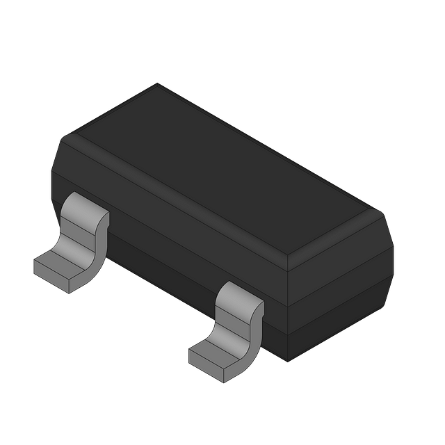
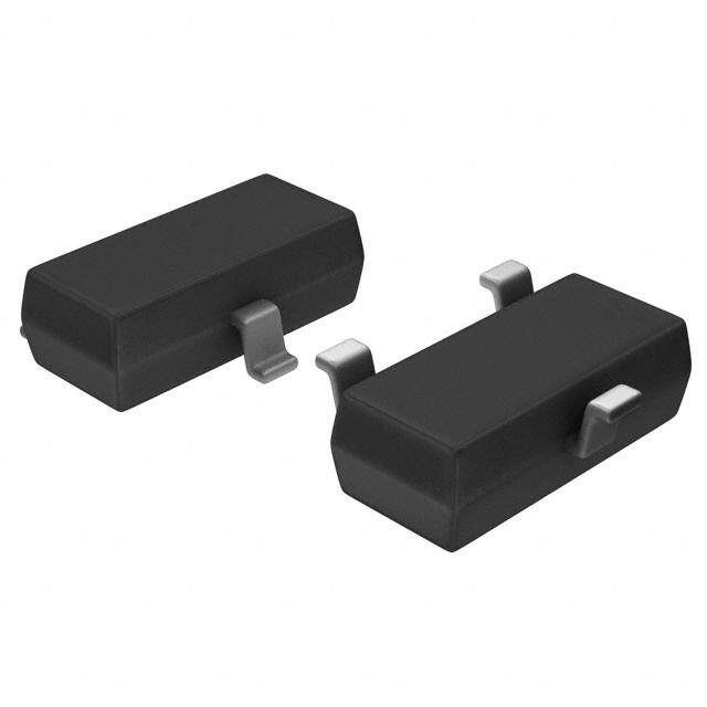
ICGOO电子元器件商城为您提供PMBD7100,215由NXP Semiconductors设计生产,在icgoo商城现货销售,并且可以通过原厂、代理商等渠道进行代购。 PMBD7100,215价格参考¥0.13-¥0.16。NXP SemiconductorsPMBD7100,215封装/规格:二极管 - 整流器 - 阵列, Diode Array 1 对共阴极 标准 100V 215mA(DC) 表面贴装 TO-236-3,SC-59,SOT-23-3。您可以下载PMBD7100,215参考资料、Datasheet数据手册功能说明书,资料中有PMBD7100,215 详细功能的应用电路图电压和使用方法及教程。
型号为PMBD7100,215的器件由品牌Nexperia USA Inc.生产,属于二极管中的整流器阵列类别。该器件主要由两个独立的高速开关二极管组成,适用于需要高效、快速切换的应用场景。

PMBD7100,215的典型应用场景包括:

1. 电源管理电路:用于AC-DC转换器或DC-DC转换器中,作为整流或续流二极管使用,提高电源效率。
2. 信号整流与钳位电路:在模拟或数字信号处理中,用于对信号进行整流、限幅或保护后级电路。
3. 电机驱动电路:用于抑制电机反向电动势,保护开关元件(如MOSFET)免受电压尖峰损坏。
4. LED背光驱动:在显示设备中用于提供稳定的电流路径,确保LED亮度均匀。
5. 工业自动化和通信设备:因其高可靠性与小尺寸封装,适用于紧凑型工业控制系统和通信模块中的信号处理与保护。

该器件采用小型SOT23封装,适合高密度PCB布局,广泛应用于消费电子、汽车电子、工业控制等领域。
| 参数 | 数值 |
| 产品目录 | |
| 描述 | DIODE ARRAY 100V 215MA TO236AB整流器 DIODE SW TAPE-7 |
| 产品分类 | 二极管,整流器 - 阵列分离式半导体 |
| 品牌 | NXP Semiconductors |
| 产品手册 | |
| 产品图片 |
|
| rohs | 符合RoHS无铅 / 符合限制有害物质指令(RoHS)规范要求 |
| 产品系列 | 二极管与整流器,整流器,NXP Semiconductors PMBD7100,215- |
| 数据手册 | |
| 产品型号 | PMBD7100,215 |
| PCN封装 | |
| PCN组件/产地 | |
| PCN设计/规格 | |
| 不同If时的电压-正向(Vf) | 1.25V @ 150mA |
| 不同 Vr时的电流-反向漏电流 | 2.5µA @ 100V |
| 二极管类型 | 标准 |
| 二极管配置 | 1 对共阴极 |
| 产品 | Ultra Fast Recovery Rectifiers |
| 产品种类 | 整流器 |
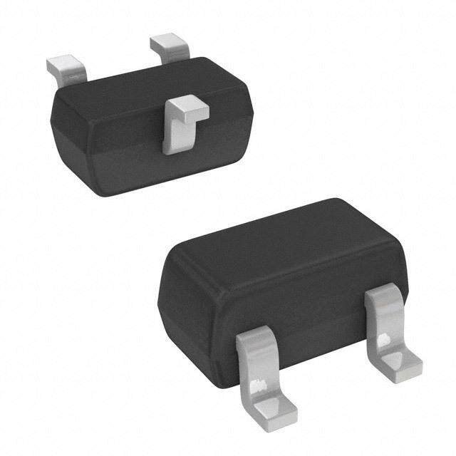
| 供应商器件封装 | SOT-23 (TO-236AB) |
| 其它名称 | 568-6476-1 |
| 包装 | 剪切带 (CT) |
| 反向恢复时间(trr) | 4ns |
| 反向电压 | 100 V |
| 反向电流IR | 2.5 uA |
| 商标 | NXP Semiconductors |
| 安装类型 | 表面贴装 |
| 安装风格 | SMD/SMT |
| 封装 | Reel |
| 封装/外壳 | TO-236-3,SC-59,SOT-23-3 |
| 封装/箱体 | SOT-23 |
| 工作温度范围 | + 150 C |
| 工厂包装数量 | 3000 |
| 恢复时间 | 4 ns |
| 最大工作温度 | + 150 C |
| 最大浪涌电流 | 4 A |
| 最小工作温度 | - 65 C |
| 标准包装 | 1 |
| 正向电压下降 | 1.25 V at 0.15 A |
| 正向连续电流 | 0.215 A |
| 热阻 | 360°C/W Jl |
| 电压-DC反向(Vr)(最大值) | 100V |
| 电流-平均整流(Io)(每二极管) | 215mA(DC) |
| 速度 | 快速恢复 =< 500 ns,> 200mA(Io) |
| 配置 | Dual Common Cathode |
| 零件号别名 | PMBD7100 T/R |


- 商务部:美国ITC正式对集成电路等产品启动337调查
- 曝三星4nm工艺存在良率问题 高通将骁龙8 Gen1或转产台积电
- 太阳诱电将投资9.5亿元在常州建新厂生产MLCC 预计2023年完工
- 英特尔发布欧洲新工厂建设计划 深化IDM 2.0 战略
- 台积电先进制程称霸业界 有大客户加持明年业绩稳了
- 达到5530亿美元!SIA预计今年全球半导体销售额将创下新高
- 英特尔拟将自动驾驶子公司Mobileye上市 估值或超500亿美元
- 三星加码芯片和SET,合并消费电子和移动部门,撤换高东真等 CEO
- 三星电子宣布重大人事变动 还合并消费电子和移动部门
- 海关总署:前11个月进口集成电路产品价值2.52万亿元 增长14.8%

PDF Datasheet 数据手册内容提取
Important notice Dear Customer, On 7 February 2017 the former NXP Standard Product business became a new company with the tradename Nexperia. Nexperia is an industry leading supplier of Discrete, Logic and PowerMOS semiconductors with its focus on the automotive, industrial, computing, consumer and wearable application markets In data sheets and application notes which still contain NXP or Philips Semiconductors references, use the references to Nexperia, as shown below. Instead of http://www.nxp.com, http://www.philips.com/ or http://www.semiconductors.philips.com/, use http://www.nexperia.com Instead of sales.addresses@www.nxp.com or sales.addresses@www.semiconductors.philips.com, use salesaddresses@nexperia.com (email) Replace the copyright notice at the bottom of each page or elsewhere in the document, depending on the version, as shown below: - © NXP N.V. (year). All rights reserved or © Koninklijke Philips Electronics N.V. (year). All rights reserved Should be replaced with: - © Nexperia B.V. (year). All rights reserved. If you have any questions related to the data sheet, please contact our nearest sales office via e-mail or telephone (details via salesaddresses@nexperia.com). Thank you for your cooperation and understanding, Kind regards, Team Nexperia
DISCRETE SEMICONDUCTORS DATA SHEET dbook, halfpage M3D088 PMBD7100 High-speed double diode Product data sheet 2003 Nov 07
NXP Semiconductors Product data sheet High-speed double diode PMBD7100 FEATURES PINNING • Small plastic SMD package PIN DESCRIPTION • High switching speed: max. 4 ns 1 anode (a1) • Continuous reverse voltage: max. 100 V 2 anode (a2) • Repetitive peak reverse voltage: max. 100 V 3 common connection • Repetitive peak forward current: max. 450 mA. APPLICATIONS • High-speed switching in thick and thin-film circuits. DESCRIPTION handbook, halfpage 3 3 The PMBD7100 consists of two high-speed switching diodes with common cathodes, fabricated in planar technology, and encapsulated in the small SOT23 SMD 1 2 plastic package. 1 2 MARKING Top view MAM383 TYPE NUMBER MARKING CODE(1) PMBD7100 *3A Note 1. * = p: made in Hong Kong. * = t: made in Malaysia. Fig.1 Simplified outline (SOT23) and symbol. * = W: made in China. ORDERING INFORMATION PACKAGE TYPE NUMBER NAME DESCRIPTION VERSION PMBD7100 − plastic surface mounted package; 3 leads SOT23 2003 Nov 07 2
NXP Semiconductors Product data sheet High-speed double diode PMBD7100 LIMITING VALUES In accordance with the Absolute Maximum Rating System (IEC 60134). SYMBOL PARAMETER CONDITIONS MIN. MAX. UNIT Per diode V repetitive peak reverse voltage − 100 V RRM V continuous reverse voltage − 100 V R I continuous forward current single diode loaded; see Fig.2; note 1 − 215 mA F double diode loaded; see Fig.2; note 1 − 125 mA I repetitive peak forward current − 450 mA FRM I non-repetitive peak forward current square wave; T = 25 °C prior to surge; FSM j see Fig.4 t = 1 µs − 4 A p t = 1 ms − 1 A p t = 1 s − 0.5 A p P total power dissipation T = 25 °C; note 1 − 250 mW tot amb T storage temperature −65 +150 °C stg T junction temperature − 150 °C j Note 1. Device mounted on an FR4 printed-circuit board. 2003 Nov 07 3
NXP Semiconductors Product data sheet High-speed double diode PMBD7100 ELECTRICAL CHARACTERISTICS T = 25 °C unless otherwise specified. amb SYMBOL PARAMETER CONDITIONS MAX. UNIT Per diode V forward voltage see Fig.3 F I = 1 mA 715 mV F I = 10 mA 855 mV F I = 50 mA 1 V F I = 150 mA 1.25 V F I reverse current see Fig.5 R V = 25 V 30 nA R V = 100 V 2.5 µA R V = 25 V; T = 150 °C 60 µA R j V = 100 V; T = 150 °C 100 µA R j C diode capacitance V = 0 V; f = 1 MHz; see Fig.6 1.5 pF d R t reverse recovery time when switched from I = 10 mA to 4 ns rr F I = 10 mA; R = 100 Ω; measured at R L I = 1 mA; see Fig.7 R V forward recovery voltage when switched from I = 10 mA to t = 20 nA; 1.75 V fr F r see Fig.8 THERMAL CHARACTERISTICS SYMBOL PARAMETER CONDITIONS VALUE UNIT R thermal resistance from junction to tie-point 360 K/W th j-tp R thermal resistance from junction to ambient note 1 500 K/W th j-a Note 1. Device mounted on an FR4 printed-circuit board. 2003 Nov 07 4
NXP Semiconductors Product data sheet High-speed double diode PMBD7100 GRAPHICAL DATA MBD033 MDB820 300 300 handIbFook, halfpage IF (mA) 250 (mA) 200 200 single diode loaded 150 double diode loaded 100 100 (1) (2) (3) 50 0 0 0 100 T a m b ( o C) 200 0 0.5 1.0 1.5 VF (V) 2.0 (1) Tj = 150 °C; typical values. Device mounted on an FR4 printed-circuit board. (2) Tj = 25 °C; typical values. (3) Tj = 25 °C; maximum values. Fig.2 Maximum permissible continuous forward current as a function of ambient Fig.3 Forward current as a function of temperature. forward voltage. 102 MBG704 handbook, full pagewidth IFSM (A) 10 1 10−1 1 10 102 103 tp (µs) 104 Based on square wave currents. Tj = 25 °C prior to surge. Fig.4 Maximum permissible non-repetitive peak forward current as a function of pulse duration. 2003 Nov 07 5
NXP Semiconductors Product data sheet High-speed double diode PMBD7100 102 MDB821 0.8 MDB822 handbook, halfpage handbook, halfpage IR Cd (µA) (pF) (1) 10 0.6 (2) (3) 1 0.4 10-1 0.2 10-2 10−3 0 0 50 100 150 Tj (°C) 200 0 5 10 VR (V) 15 (1) VR = 100 °C; maximum values. (2) VR = 100 °C; typical values. (3) VR = 25 °C; typical values. f = 1 MHz; Tj = 25 °C. Fig.5 Reverse current as a function of junction Fig.6 Diode capacitance as a function of reverse temperature. voltage; typical values. 2003 Nov 07 6
NXP Semiconductors Product data sheet High-speed double diode PMBD7100 handbook, full pagewidth tr tp t D.U.T. 10% RS = 50Ω IF SAMPLING IF trr t OSCILLOSCOPE V = VR I F x RS R i = 50Ω 90% (1) VR MGA881 input signal output signal (1) IR = 1 mA. Fig.7 Reverse recovery voltage test circuit and waveforms. I 1 kΩ 450 Ω I V 90% R = 50Ω S D.U.T. OSCILLOSCOPE Vfr R i = 50Ω 10% MGA882 t t tr tp input output signal signal Fig.8 Forward recovery voltage test circuit and waveforms. 2003 Nov 07 7
NXP Semiconductors Product data sheet High-speed double diode PMBD7100 PACKAGE OUTLINE Plastic surface mounted package; 3 leads SOT23 D B E A X HE v M A 3 Q A A1 1 2 c e1 bp w M B Lp e detail X 0 1 2 mm scale DIMENSIONS (mm are the original dimensions) UNIT A mAa1x. bp c D E e e1 HE Lp Q v w 1.1 0.48 0.15 3.0 1.4 2.5 0.45 0.55 mm 0.1 1.9 0.95 0.2 0.1 0.9 0.38 0.09 2.8 1.2 2.1 0.15 0.45 OUTLINE REFERENCES EUROPEAN ISSUE DATE VERSION IEC JEDEC EIAJ PROJECTION 97-02-28 SOT23 TO-236AB 99-09-13 2003 Nov 07 8
NXP Semiconductors Product data sheet High-speed double diode PMBD7100 DATA SHEET STATUS DOCUMENT PRODUCT DEFINITION STATUS(1) STATUS(2) Objective data sheet Development This document contains data from the objective specification for product development. Preliminary data sheet Qualification This document contains data from the preliminary specification. Product data sheet Production This document contains the product specification. Notes 1. Please consult the most recently issued document before initiating or completing a design. 2. The product status of device(s) described in this document may have changed since this document was published and may differ in case of multiple devices. The latest product status information is available on the Internet at URL http://www.nxp.com. DISCLAIMERS above those given in the Characteristics sections of this document is not implied. Exposure to limiting values for General ⎯ Information in this document is believed to be extended periods may affect device reliability. accurate and reliable. However, NXP Semiconductors does not give any representations or warranties, Terms and conditions of sale ⎯ NXP Semiconductors expressed or implied, as to the accuracy or completeness products are sold subject to the general terms and of such information and shall have no liability for the conditions of commercial sale, as published at consequences of use of such information. http://www.nxp.com/profile/terms, including those pertaining to warranty, intellectual property rights Right to make changes ⎯ NXP Semiconductors infringement and limitation of liability, unless explicitly reserves the right to make changes to information otherwise agreed to in writing by NXP Semiconductors. In published in this document, including without limitation case of any inconsistency or conflict between information specifications and product descriptions, at any time and in this document and such terms and conditions, the latter without notice. This document supersedes and replaces all will prevail. information supplied prior to the publication hereof. No offer to sell or license ⎯ Nothing in this document Suitability for use ⎯ NXP Semiconductors products are may be interpreted or construed as an offer to sell products not designed, authorized or warranted to be suitable for that is open for acceptance or the grant, conveyance or use in medical, military, aircraft, space or life support implication of any license under any copyrights, patents or equipment, nor in applications where failure or malfunction other industrial or intellectual property rights. of an NXP Semiconductors product can reasonably be expected to result in personal injury, death or severe Export control ⎯ This document as well as the item(s) property or environmental damage. NXP Semiconductors described herein may be subject to export control accepts no liability for inclusion and/or use of NXP regulations. Export might require a prior authorization from Semiconductors products in such equipment or national authorities. applications and therefore such inclusion and/or use is at Quick reference data ⎯ The Quick reference data is an the customer’s own risk. extract of the product data given in the Limiting values and Applications ⎯ Applications that are described herein for Characteristics sections of this document, and as such is any of these products are for illustrative purposes only. not complete, exhaustive or legally binding. NXP Semiconductors makes no representation or warranty that such applications will be suitable for the specified use without further testing or modification. Limiting values ⎯ Stress above one or more limiting values (as defined in the Absolute Maximum Ratings System of IEC 60134) may cause permanent damage to the device. Limiting values are stress ratings only and operation of the device at these or any other conditions 2003 Nov 07 9
NXP Semiconductors Customer notification This data sheet was changed to reflect the new company name NXP Semiconductors. No changes were made to the content, except for the legal definitions and disclaimers. Contact information For additional information please visit: http://www.nxp.com For sales offices addresses send e-mail to: salesaddresses@nxp.com © NXP B.V. 2009 All rights are reserved. Reproduction in whole or in part is prohibited without the prior written consent of the copyright owner. The information presented in this document does not form part of any quotation or contract, is believed to be accurate and reliable and may be changed without notice. No liability will be accepted by the publisher for any consequence of its use. Publication thereof does not convey nor imply any license under patent- or other industrial or intellectual property rights. Printed in The Netherlands R76/01/pp10 Date of release: 2003 Nov 07 Document order number: 9397 750 12001