ICGOO在线商城 > 集成电路(IC) > PMIC - PFC(功率因数修正) > PFS714EG
 Datasheet下载
- 型号: PFS714EG
- 制造商: Power Integrations
- 库位|库存: xxxx|xxxx
- 要求:
| 数量阶梯 | 香港交货 | 国内含税 |
| +xxxx | $xxxx | ¥xxxx |
查看当月历史价格
查看今年历史价格
PFS714EG产品简介:
ICGOO电子元器件商城为您提供PFS714EG由Power Integrations设计生产,在icgoo商城现货销售,并且可以通过原厂、代理商等渠道进行代购。 PFS714EG价格参考。Power IntegrationsPFS714EG封装/规格:PMIC - PFC(功率因数修正), PFC IC Continuous Conduction (CCM) 24kHz ~ 95kHz eSIP-7G。您可以下载PFS714EG参考资料、Datasheet数据手册功能说明书,资料中有PFS714EG 详细功能的应用电路图电压和使用方法及教程。
Power Integrations 的 PFS714EG 是一款集成功率因数校正(PFC)功能的电源管理 IC(PMIC),主要用于提高电源系统的功率因数,减少谐波失真,满足国际能效标准。

主要应用场景包括:

1. 消费类电子产品电源适配器:如笔记本电脑、液晶电视、游戏机等设备的电源适配器中,用于提升功率因数,实现高效、低功耗运行。

2. 工业电源系统:用于工业设备中的开关电源(SMPS),如变频器、伺服驱动器、工业自动化设备等,确保输入电流波形与电压同步,提高能源利用率。

3. 家电产品:如空调、洗衣机、电磁炉等大功率家电的电源部分,使用 PFS714EG 可改善功率因数,降低电网污染,符合能效法规。

4. LED 照明电源:用于高功率 LED 灯具的驱动电源中,实现高功率因数和高效率,适用于商业和工业照明系统。

5. 服务器和通信设备电源:在数据中心服务器、网络设备的电源模块中,PFS714EG 有助于满足严格的能效认证要求(如 80 PLUS)。

该芯片采用高集成度设计,支持连续导通模式(CCM)PFC,具备过压、过流、过热等多重保护功能,适用于宽输入电压范围,适用于中高功率电源系统设计。
| 参数 | 数值 |
| 产品目录 | 集成电路 (IC)半导体 |
| 描述 | IC PFC CTLR 385W 90V ESIP功率因数校正 - PFC PFC w/ Pwr Mosfet 385 W MAX 90 VAC |
| 产品分类 | |
| 品牌 | Power Integrations |
| 产品手册 | |
| 产品图片 |
|
| rohs | 符合RoHS无铅 / 符合限制有害物质指令(RoHS)规范要求 |
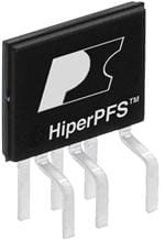
| 产品系列 | 电源管理 IC,功率因数校正 - PFC,Power Integrations PFS714EGHiperPFS™ |
| 数据手册 | |
| 产品型号 | PFS714EG |
| 产品种类 | 功率因数校正 - PFC |
| 供应商器件封装 | eSIP-7G |
| 其它名称 | 596-1411 |
| 包装 | 管件 |
| 参考设计库 | http://www.digikey.com/rdl/4294959902/4294959897/735 |
| 商标 | Power Integrations |
| 安装类型 | 通孔 |
| 安装风格 | Through Hole |
| 封装 | Tube |
| 封装/外壳 | 7-SIP,6 引线,裸露焊盘,成形引线 |
| 封装/箱体 | eSip-7G |
| 工作温度 | -40°C ~ 125°C |
| 工厂包装数量 | 48 |
| 开关频率 | 24 kHz to 95 kHz |
| 最大工作温度 | + 150 C |
| 最小工作温度 | - 40 C |
| 标准包装 | 48 |
| 模式 | 连续导电(CCM) |
| 电压-电源 | 10 V ~ 12 V |
| 电流-启动 | - |
| 频率-开关 | 24kHz ~ 95kHz |


- 商务部:美国ITC正式对集成电路等产品启动337调查
- 曝三星4nm工艺存在良率问题 高通将骁龙8 Gen1或转产台积电
- 太阳诱电将投资9.5亿元在常州建新厂生产MLCC 预计2023年完工
- 英特尔发布欧洲新工厂建设计划 深化IDM 2.0 战略
- 台积电先进制程称霸业界 有大客户加持明年业绩稳了
- 达到5530亿美元!SIA预计今年全球半导体销售额将创下新高
- 英特尔拟将自动驾驶子公司Mobileye上市 估值或超500亿美元
- 三星加码芯片和SET,合并消费电子和移动部门,撤换高东真等 CEO
- 三星电子宣布重大人事变动 还合并消费电子和移动部门
- 海关总署:前11个月进口集成电路产品价值2.52万亿元 增长14.8%


PDF Datasheet 数据手册内容提取
PFS704-729EG HiperPFS Family High Power PFC Controller with Integrated High-Voltage MOSFET Key Benefits Output Power Table • Single chip solution for boost power factor correction (PFC) • EN61000-3-2 Class C and D compliant Maximum Continuous Peak Output Power • High light load efficiency at 10% and 20% load Product Output Power Rating at Rating at 90 VAC 90 VAC • >95% efficiency from 10% load to full load • <130 mW no-load consumption at 230 VAC with output in PFS704EG 110 W 120 W regulation PFS706EG 140 W 150 W • <50 mW no-load consumption at 230 VAC in remote off state PFS708EG 190 W 205 W • Frequency adjusted over line voltage, and line cycle PFS710EG 240 W 260 W • Spread-spectrum across >60 kHz window to simplify EMI filtering requirements PFS712EG 300 W 320 W • Lower boost inductance PFS713EG 300 W 320 W • Provides up to 1 kW peak output power PFS714EG 350 W 385 W • >1 kW peak power delivery in power limit voltage regulation PFS716EG 388 W 425 W mode Maximum Continuous • High integration allows smaller form factor, higher power density Peak Output Power Product Output Power Rating at designs Rating at 180 VAC 180 VAC • Incorporates control, gate driver, and high-voltage power PFS723EG 255 W 280 W MOSFET • Internal current sense reduces component count and system PFS724EG 315 W 350 W losses PFS725EG 435 W 480 W • Protection features include: UV, OV, OTP, brown-in/out, cycle- PFS726EG 540 W 600 W by-cycle current limit, and power limiting for overload protection PFS727EG 675 W 750 W • Halogen free and RoHS compliant PFS728EG 810 W 900 W Applications PFS729EG 900 W 1000 W • PC • High power adaptors Table 1. Output Power Table (see Notes on page 9) • Printer • High power LED lighting • LCD TV • Industrial and appliance • Video game consoles • Generic PFC converters + VCC D V VCC CONTROL DC AC HiperPFS FB OUT IN S G Figure 1. Typical Application Schematic. PI-6021-110810 www.power.com June 2015 This Product is Covered by Patents and/or Pending Patent Applications.
PFS704-729EG Section List Description ...................................................................................................................................................................3 Product Highlights .......................................................................................................................................................3 Pin Functional Description .........................................................................................................................................4 Pin Configuration ......................................................................................................................................................4 Functional Block Diagram ........................................................................................................................................4 Functional Description ................................................................................................................................................5 Output Power Table .................................................................................................................................................9 Application Example ............................................................................................................................................10-11 Design, Assembly, and Layout Considerations ....................................................................................................12 Absolute Maximum Ratings .....................................................................................................................................19 Parameter Table ................................................................................................................................................19-25 Typical Performance Characteristics ......................................................................................................................26 Package Details .........................................................................................................................................................27 Part Ordering Information.........................................................................................................................................28 Part Marking Information .........................................................................................................................................28 2 Rev. G 06/15 www.power.com
PFS704-729EG Description Product Highlights The HiperPFS™ device family members incorporate a continuous conduction mode (CCM) boost PFC controller, gate Protected Power Factor Correction Solution driver, and high voltage power MOSFET in a single, low-profile • Incorporates high-voltage power MOSFET, controller, and gate eSIP™ power package that is able to provide near unity input driver power factor. The HiperPFS devices eliminate the PFC • EN61000-3-2 Class D compliance converter’s need for external current sense resistors, the power • Integrated protection features reduce external component count loss associated with those components, and leverages an • Accurate built-in brown-in/out protection innovative control technique that adjusts the switching frequency • Accurate built-in undervoltage (UV) protection over output load, input line voltage, and even input line cycle. • Accurate built-in overvoltage (OV) protection This control technique is designed to maximize efficiency over • Hysteretic thermal shutdown (OTP) the entire load range of the converter, particularly at light loads. • Internal power limiting function for overload protection Additionally, this control technique significantly minimizes the • Cycle-by-cycle power switch current limit EMI filtering requirements due to its wide-bandwidth spread • No external current sense required spectrum effect. HiperPFS includes Power Integrations’ • Provides “lossless” internal sensing via sense-FET standard set of comprehensive protection features, such as • Reduces component count and system losses integrated soft-start, UV, OV, brown-in/out, and hysteretic thermal • Minimizes high current gate drive loop area shutdown. HiperPFS also provides cycle-by-cycle current limit • Minimizes output overshoot and stresses during start-up for the power MOSFET, power limiting of the output for over- • Integrated power limit and frequency soft start load protection, and pin-to-pin short-circuit protection. • Improve dynamic response • Input line feed-forward gain adjustment for constant loop HiperPFS’s innovative variable-frequency continuous conduction gain across entire input voltage range mode of operation (VF-CCM) minimizes switching losses by • Eliminates up to 40 discrete components for higher reliability maintaining a low average switching frequency, while also and lower cost varying the switching frequency in order to suppress EMI, the Intelligent Solution for High Efficiency and Low EMI traditional challenge with continuous-conduction-mode solutions. Systems using HiperPFS typically reduce the total X • Continuous conduction mode PFC uses novel constant volt/ amp-second control engine and Y capacitance requirements of the converter, the inductance of both the boost choke and EMI noise suppression chokes, • High efficiency across load using a UF boost diode reducing overall system size and cost. Additionally, compared • Low cost EMI filter with designs that use discrete MOSFETs and controllers, • Universal input device (PFS704 – PFS716) utilize frequency sliding technique for light load efficiency improvements HiperPFS devices dramatically reduce component count and board footprint while simplifying system design and enhancing • >95% efficiency from 10% load to full load at low line input voltage reliability. The innovative variable-frequency, continuous conduction mode controller enables the HiperPFS to realize all • >96% efficiency from 10% load to full load at high line input voltage of the benefits of continuous-conduction mode operation while leveraging low-cost, small, simple EMI filters. • High line input device (PFS723 – PFS729) maintain higher average switching frequency to minimize boost inductance and core size Many regions mandate high power factor for many electronic products with high power requirements. These rules are • >94% efficiency from 10% load to full load combined with numerous application-specific standards that • Variable switching frequency to simplify EMI filter design require high power supply efficiency across the entire load • Varies over line input voltage to maximize efficiency and minimize EMI filter requirements range, from full load to as low as 10% load. High efficiency at light load is a challenge for traditional PFC approaches in which • Varies with input line cycle voltage by >60 kHz to maximize spread spectrum effect fixed MOSFET switching frequencies cause fixed switching losses on each cycle, even at light loads. HiperPFS simplifies Advanced Package for High Power Applications compliance with new and emerging energy-efficiency standards • Up to 1 kW peak output power capability in a highly compact over a broad market space in applications such as PCs, LCD package TVs, notebooks, appliances, pumps, motors, fans, printers, and • Simple clip mounting to heat sink LED lighting. • Can be directly connected to heat sink with insulation pad • Provides thermal resistance equivalent to a TO-220 HiperPFS advanced power packaging technology and high • Staggered pin arrangement for simple routing of board traces efficiency simplifies the complexity of mounting the package and high voltage creepage requirements and thermal management, while providing very high power • Single package solution for PFC converter reduces assembly capabilities in a single compact package; these devices are costs and layout size suitable for PFC applications from 75 W to 1 kW 3 www.power.com Rev. G 06/15
PFS704-729EG Pin Functional Description SIGNAL GROUND (G) Pin: Discrete components used in the feedback circuit, including VOLTAGE MONITOR (V) Pin: loop compensation, decoupling capacitors for the supply (VCC) The V pin is tied to the rectified AC rail through an external and line-sense (V) must be referenced to the G pin. The resistor. Internal circuitry detects the peak of the input line SIGNAL GROUND pin must not be tied to the SOURCE pin. voltage which resembles a full-wave rectified waveform. The rectified high-voltage bus is connected directly to the V pin SOURCE (S) Pin: voltage through a large resistor (4 MW for PFS70x and PFS71x; This pin is the source connection of the power switch. 9 MW for PFS72x) to minimize power dissipation and standby power consumption. A small ceramic capacitor (0.1 mF for DRAIN (D) Pin: PFS70x and PFS71x; 0.047 mF for PFS72x) is required from the This is the tab and drain connection of the internal power switch. VOLTAGE MONITOR pin to SIGNAL GROUND pin to bypass any switching noise present on the rectified bus. This pin also features both brown-in and brown-out protection. E Package (eSIP-7G) Exposed Metal (On Edge) FEEDBACK (FB) Pin: Internally Connected Exposed Metal to GROUND Pin (On Edge) The FEEDBACK pin is high input-impedance reference terminal Internally that connects to a feedback resistor network. This pin will also Connected to feature fast overvoltage and undervoltage detection circuitry DRAIN Pin that will disengage the internal power MOSFET in the event of a system fault. A 10 nF capacitor is required between the Exposed Pad FEEDBACK to SIGNAL GROUND pins; this capacitor must be (Backside) Internally placed very close to the device on the PCB to bypass any Connected to switching noise. This pin is also used for loop compensation. DRAIN Pin (see eSIP-7G 1 23 45 7 7 54 32 1 Package BIAS POWER (VCC) Pin: VFVGS D D SGVFV Drawing) This is a 10-12 VDC bias supply used to power the IC. The bias BCC CCB PI-5334-083110 voltage must be externally clamped to prevent the VCC pin from exceeding 15 VDC. Figure 2. Pin Configuration. VOLTAGE MONITOR (V) BIAS POWER (VCC) DRAIN (D) INPUT LINE INTERFACE INTERNAL + Peak SUPPLY - VCC+ Detector OTP SOFT MONIVPK Input UV “Off-time derived with START (IUV-/IUV+) 6 V Input Voltage constant Volt-Sec Emulation + VO-VIN C - INT 7 kHz Filter V is a function of the error-voltage (V) and is used to reduce the average o((PVpOFOeFFSFrFa7 t=0in 40g-. 78fr1 eV6q )uf.o ern PcFy SaIn7st2 ea3r -fnu7an2lc9t)i.TonrEa onrrfso ocrou-AntpEmduuptc lpitfaoienwrceer fIoVrP iKncreaVOFFsed effiFcreiequnSenlciVdcEeyy VOFF +C-Coommppaarraattoorr Latch FOBOTIVnP/UpVut UV DVriCvCer SFeEnTse MPOoSwFeErT RefVerence VE + FEEDBACK (FB) REF + 1 kHz - LEB IS - Filter TIMER SUPERVISOR M is the switch current siesOn Nfsuen cstcioanle o ffa pcetoark w lihniec h The irnetgeurnlaatle dse trhivee odu etprruotr -vvooltlataggee (VE) + IOCP + voltage derived from IVIN OCP - FBOV - Fast OV MON IS CINT Comparator FB / FBUV OFF + - UV Comparator SIGNAL GROUND (G) SOURCE (S) PI-5333-113010 Figure 3. Functional Block Diagram. 4 Rev. G 06/15 www.power.com
PFS704-729EG Functional Description 0 1 6 1 The HiperPFS is a variable switching frequency boost PFC VE 5-11 soonl-utitmioen .a nMdo creo nsspteacnitfi cvoalllty-,s iet ceomnpdl ooyffs- taim ceo ncostnatnrot la amlgpo-rsitehcmo.n d Latch IS dt PI-533 RESET This algorithm is used to regulate the output voltage and shape V OFF the input current to comply with regulatory harmonic current (V -V )dt limits (high power factor). Integrating the switch current and Latch OUT IN controlling it to have a constant amp-sec product over the SET on-time of the switch allows the average input current to follow Gate the input voltage. Integrating the difference between the output Drive (Q) and input voltage maintains a constant volt-second balance Maximum ON-time dictated by the electro-magnetic properties of the boost inductor Minimum Timing and thus regulates the output voltage and power. OFF-time Supervisor More specifically, the control technique sets constant volt- seconds for the off-time (t ). The off-time is controlled such OFF Figure 4. Idealized Converter Waveforms. that: cycle on-time. Internally the difference between the input and (1) output voltage is derived and the resultant is scaled, integrated, and compared to a voltage reference (V ) to determine the Since the volt-seconds during the on-time must equal the cycle off-time. Careful selection of the inOtFeFrnal scaling factors volt-seconds during the off-time, to maintain flux equilibrium in produce input current waveforms with very low distortion and the PFC choke, the on-time (t ) is controlled such that: high power factor. ON (2) The input voltage is internally synthesized using the switch duty cycle and a 7 kHz low pass filter. This synthesized input voltage The controller also sets a constant value of charge during each representation is subtracted from a fixed reference voltage (6 V) on-cycle of the power MOSFET. The charge per cycle is varied to derive a current source proportional to (V -V ). Please refer to gradually over many switching cycles in response to load Figure 3. O IN changes so it can be regarded as substantially constant for a half line cycle. With this constant charge (or amp-second) Line Feed-Forward Scaling Factor (M ) ON control, the following relationship is therefore also true: The VOLTAGE MONITOR (V) pin current is used internally to derive the peak of the input line voltage which is used to scale (3) the gain of the current sense signal through the M variable. ON This contribution is required to reduce the dynamic range of the Substituting t from (2) into (3) gives: control feedback signal as well maintain a constant loop gain ON over the operating input line range. This line-sense feed- (4) forward gain adjustment is proportional to the square of the peak rectified AC line voltage and is adjusted as a function of V The relationship of (4) demonstrates that by controlling a constant pin current. The line-sense feed-forward gain is also important amp-second on-time and constant volt-second off-time, the input in providing a switch power limit over the input line range. current I is proportional to the input voltage V , therefore Besides modifying brown- in/out thresholds, the V pin resistor IN IN providing the fundamental requirement of power factor correction. also affects power limit of the device This control produces a continuous mode power switch current This characteristic is optimized to maintain a relatively constant waveform that varies both in frequency and peak current value internal error-voltage level at full load from an input line of 100 across a line half-cycle to produce an input current proportional to 230 VAC input (PFS704-716). to the input voltage. Beyond the specified peak power rating of the device, the Control Engine internal power limit feature will regulate the output voltage The controller features a low bandwidth error-amplifier which below the set regulation threshold as a function of output connects its non-inverting terminal to an internal voltage overload beyond the peak power rating. Figure 5 illustrates the reference of 6 V. The inverting terminal of the error-amplifier is typical regulation characteristic as function of load. available on the external FEEDBACK pin which connects to the external feedback resistor divider, transient load speed-up and Soft-Start with Pin-to-Pin Short-Circuit Protection compensation networks to regulate the output voltage. Since the FEEDBACK pin is the interface for output voltage regulation (resistor voltage divider to output voltage) as well as The internal sense-FET switch current is integrated and scaled loop compensation (series RC), the typical application circuit of by the input voltage peak detector current sense gain (M ) and the HiperPFS requires an external transistor network to overcome ON compared with the error-amplifier signal (V ) to determine the the inherently slow feedback loop response. Specifically, an E 5 www.power.com Rev. G 06/15
PFS704-729EG 1.2 ge 010 a 13 ut Volthold 1 PI-6216-1 SSeoCqfhtu-eSecntkacret ps0.8 Outhre et n T0.6 zed to Segulatio0.4 VVCCICsC +> NO C6u mrArAepn pVtl yPS iinnk VDoelttaegcet IPnpeaukt maliR0.2 YES r o Apply 0.5 μA N on FB to 0 Check Open FB NO Start 0 0.2 0.4 0.6 0.8 1 1.2 1.4 Is VFB > FBOFF Converter Normalized to Peak Power Rating Figure 5. Typical Normalized Output Voltage Characteristics as Function of Is YES Normalized Peak Load Rating VFB a>n FdBOFF NO VFB < FBOV 6 RmeAm Vo vPein SOlevwe rP Soowfet-rS-Ltaimrtit Current Sink Duration VCCegatlo VCC+ YES V NO Is IV > IUV+ )E V ( e tSTART-DELAY YES g a PI-5337-110910 tloV tSOFT -ro ~5 V Figure 7. Start-Up Sequence. rrE la threshold the V pin holds the 6 mA current sink indefinitely until n re the FEEDBACK pin is above the FB . If the FEEDBACK pin tn OFF I voltage is above FB , the IC releases the current source and OFF t resumes with normal soft-start and operation. Figure 7 PI-5336-110810 illustrates this sequence. Figure 6. Power Limit Soft-Start Function. Timing Supervisor and Operating Frequency Range Since the controller is expected to operate with a variable NPN and PNP transistor are tied between the output voltage switching frequency over the line frequency half-cycle, typically divider resistors to limit the maximum overshoot and under- spanning a range of 24 – 95 kHz, the controller also features a shoot during a load transient response. To reduce switch and timing supervisor function which monitors and limits the output diode current stress at start-up, the HiperPFS slews the maximum switch on-time and off-time as well as ensures a internal error-voltage from zero to its steady-state value at minimum cycle off-time. The timer supervisor limits the normal start-up. Figure 6 illustrates the relative relationship between operating frequency range for loads in excess of 10% of the the application of V and power limit soft-start function through device peak power rating. CC the internal error-voltage. Figure 8a shows the typical half-line frequency profile of the The error-voltage has a controlled slew rate of 0.25 V/ms at device switching frequency as a function of input voltage at start-up, corresponding to the t time duration for a full scale peak load conditions. Figure 8b shows for a given line condition SOFT error voltage of 5 V. the effect of EcoSmart to the switching frequency as a function of load (PFS704-716). The switching frequency is not a function The beginning of soft-start is gated by the V , I and of boost choke inductance. CC+ UV+ FEEDBACK pin voltage thresholds in the sequence described below. Once the applied V is above the V threshold, the EcoSmart CC CC+ sensed V pin current is above I and the feedback pin voltage The PFS704-716 controllers includes an EcoSmart mode UV+ is above FB , the IC applies a ~6 mA current sink through the wherein the internal error signal (V ) is used to detect the OFF E VOLTAGE MONITOR pin and checks that the FEEDBACK pin converter output power. Since the internal error-signal is voltage is still above the FB threshold. This checks to ensure directly proportional to the output power, this signal level is used OFF that the FEEDBACK and V pins are not shorted together. In the to set the average switching frequency as a function of output event that the FEEDBACK pin voltage is below the FB power. The off-time integrator control reference (V ) is OFF OFF 6 Rev. G 06/15 www.power.com
PFS704-729EG 120 10 120 V = 115 VAC Expected Frequency 10 111000 230 VAC 180 VAC 135 VAC 115 VAC 90 VAC 217-1101 111000 IN 100% Peak Load RanRgea taetd P Leoaakd 218-1029 6 6 z) 90 PI- z) 90 PI- H H k 80 k 80 y ( 70 y ( 70 75% Peak Load c c n n e 60 e 60 50% Peak Load u u q 50 q 50 e e r r F 40 F 40 25% Peak Load 30 30 20 20 Peak Load 10 10 0 45 90 135 180 0 45 90 135 180 Line Conduction Angle (°C) Line Conduction Angle (°C) Figure 8. (a) Frequency Variation Over Line Half-Cycle as a Function of Input Voltage (b) Frequency Variation Over Line Half-Cycle as a Function of Load. ~5 V ~5 V PFS704-716 PFS704-716 V < 140 VAC V VFFO~2.5 V VPINF >S 710740- 7V1A6C IN 0 = VE ta ~1.25 V FFO~2.5 V V ~0.8 V PFS723-729 ~4.8 V ~5 V ~140 VAC ~170 VAC VE (full power) VIN PI-5338-021711 Figure 9. V vs. V and V vs. Input Voltage. OFF E OFF controlled with respect to the internal error-voltage level (output VOLTAGE MONITOR pin exceeds the I threshold for a V(OFF) power) to allow the converter to maintain output voltage duration exceeding approximately (1 ms), the IC disables the regulation and relatively flat conversion efficiency between 10% internal MOSFET for the entire duration that the V pin current is to 100% of rated load which is essential to meet many efficiency above I . In normal operation, if the current through the V V(OFF) directives. pin exceeds the I threshold for a duration exceeding t , V(OFF) V(OFF) the IC will re-initiate the start-up sequence. The degree of frequency slide is also controlled as a function of peak input line voltage, at high input line the maximum off-time Brown-In Protection (I ) UV+ voltage reference at zero error-voltage will be approximately 1/2 The VOLTAGE MONITOR pin features an input line undervoltage of the maximum value at low input line conditions. detection to limit the minimum start-up voltage detected through the V pin. This detection threshold will inhibit the The lower V slope reduces the average frequency swing for device from starting at very low input AC voltage. OFF high input line operation. Brown-Out Protection (I ) UV- Protection Modes The V pin features a brown-out protection mode wherein the HiperPFS will turn-off when the V pin current is below the Line VOLTAGE MONITOR (V) Pin Shutdown UV-threshold for a period exceeding the t time period. In REFRESH The VOLTAGE MONITOR pin features a shutdown protection the event a single half-line cycle is missing (normal operating mode which can be used with the VOLTAGE MONITOR pin line frequency is 47 to 63 Hz) the brown-out protection will not resistor or external circuitry to cover system faults. During be activated. The HiperPFS shutdown in effect gradually start-up (1 V < V < 5.8 V) in the event the current through the reduces the internal error-voltage to zero volts at rate of 1 V/ms FB 7 www.power.com Rev. G 06/15
PFS704-729EG to decay the power MOSFET on-time to zero. At peak power (V ~5 V) the shutdown time will be approximately 5 ms. The intEernal error-voltage is held at 0 V for as long as the input peak IV < 48 µA voltage is below the brown-in (I ) threshold. The internal PFS704-716 UV+ error-voltage controlled slew to 0 V gradually reduces the switch P C on-time to zero to deplete energy stored in the boost choke as IO well as input EMI filter for power-down. Once the error-voltage I > 59 µA V reaches zero volts the controller is effectively in an off-state (gated by 5 ms timer) and will restart once all the conditions of soft-start are satisfied. V IN The brown-out threshold is reduced to I during start-up until ~140 VAC ~170 VAC UV-SS the FEEDBACK pin exceeds approximately 5.8 V. Temporarily PI-5470-110810 reducing the brown-out threshold prevents false turn-off at high power start-up when the voltage drop across the input bridge Figure 10. Line Dependant OCP. rectifier and filter stage may cause the rectified input to sag below the brown-out threshold. The leading edge blanking circuit inhibits the current limit Fast Output Voltage Overvoltage Protection (FB ) comparator for a short time (t ) after the power MOSFET is OV LEB The FEEDBACK pin features a means to detect an output turned on. This leading edge blanking time must be set so that overvoltage condition through the FEEDBACK pin and disables current spikes caused by capacitance and rectifier reverse the power MOSFET until the sensed output voltage falls below recovery time will not cause premature termination of the the FB threshold. A deglitch filter (~2 ms) is used to prevent MOSFET conduction. OV the controller from falsely triggering this mode. An FB event in excess of the 2 ms delay will terminate the switch cycle imOmVediately. Safe Operating Range (SOA) Mode This detection circuit also includes some hysteresis. Since the cycle-by-cycle OCP mechanism described above does not prevent the possibility of inductor current “stair- Output Voltage Undervoltage Protection (FB ) casing”, an SOA mode is required. Rapid build up of the device UV The FEEDBACK pin features an undervoltage detection to current can occur in event of inductor saturation or when the detect an output overload or a broken feedback loop. If the IC input and output voltages are equal (non or very short inductor detects the falling edge on the FEEDBACK pin that has fallen reset time). below FB threshold, it will turn-off the internal power MOSFET UV and re-initiate the start-up sequence. Similar to the FB detection, The SOA mode is triggered whenever the device reaches OV this mode has a deglitch filter of approximately 100 ms. current limit (I ) and the on-time is less than t . OCP SOA VCC Undervoltage Protection (UVLO) The SOA mode forces an off-time equal to t and pulls the OCP The BIAS POWER (VCC) pin has an undervoltage lock-out internal error-voltage (V ) down to approximately 1/2 of its set E protection which inhibits the IC from starting unless the applied value. V voltage is above the V threshold. The IC initiates a CC CC+ soft-start once the VCC pin voltage exceeds the V threshold. Open FEEDBACK Pin Protection CC+ After start-up the IC will continue to operate until the VCC pin The FEEDBACK pin also features a static current of I that is FB voltage has fallen below V level. The absolute maximum continuously sourced out of the pin to protect against a fault CC- voltage of the VCC pin is 15 V which must be externally limited related to an open FEEDBACK pin. The internal current source to prevent damage to the IC. introduces a static offset to the output regulation which must be accounted for in selecting the output feedback regulation Over-Current Protection components. The device includes a cycle-by-cycle over-current-protection (OCP) mode which protects the device in the event of a Hysteretic Thermal Shutdown catastrophic fault. The OCP mode in the PFS704-716 is input The thermal shutdown circuitry senses the controller die line dependent as shown in Figure 10. The intention of OCP in temperature. The threshold is set at 118 °C typical with a 50 °C this device is strictly protection of the internal power MOSFET hysteresis. When the die temperature rises above this threshold and is not intended to protect the converter from output (118 °C +8/-7 °C), the power MOSFET switching is disabled and short-circuit or overload fault conditions. remains disabled until the die temperature falls by ~50 °C, at which point the device will re-initiate a soft-start and start-up The PFS704-716 controller latches the high line OCP for a 1/2 sequence. line cycle and updates the OCP status after the expiration of a 5 ms block-out timer. This feature has particular benefit for hard-start after an AC line cycle drop where the peak detector may falsely detect a low input line condition even though the input is at high input line. 8 Rev. G 06/15 www.power.com
PFS704-729EG Output Power Table1 Maximum Continuous Maximum Continuous Output Power Rating at Peak Output Power Peak Output Power Product Product Output Power Rating at 90 VAC2 Rating at 90 VAC5 Rating at 180 VAC5 180 VAC4 Minimum3 Maximum PFS704EG 85 W 110 W 120 W PFS723EG 255 W 280 W PFS706EG 105 W 140 W 150 W PFS724EG 315 W 350 W PFS708EG 140 W 190 W 205 W PFS725EG 435 W 480 W PFS710EG 180 W 240 W 260 W PFS726EG 540 W 600 W PFS712EG 225 W 300 W 320 W PFS727EG 675 W 750 W PFS713EG 225 W 300 W 320 W PFS714EG 265 W 350 W 385 W PFS728EG 810 W 900 W PFS716EG 295 W 388 W 425 W PFS729EG 900 W 1000 W Table 2. Output Power Table. Notes: 1. See Design, Assembly, and Layout Considerations section. 2. Maximum practical continuous power at 90 VAC in an open-frame design with adequate heat sinking, measured at 50 °C ambient. 3. Recommended lower range of maximum continuous power for best light load efficiency; HiperPFS will operate and perform below this level. 4. Maximum practical continuous power at 180 VAC in an open-frame design with adequate heat sinking, measured at 50 °C ambient. 5. Internal output power limit. 9 www.power.com Rev. G 06/15
PFS704-729EG Application Example the high performance configuration, the thermistors should be shorted. Capacitors C14 and C21 are used for reducing the A High Efficiency, 347 W, 380 VDC Universal Input PFC loop length and area of the output circuit to reduce EMI and The circuit shown in Figure 11 is designed using a PFS714EG overshoot of voltage across the drain and source of the device from the HiperPFS family of integrated PFC controllers. MOSFET inside U1 at each switching instant. This design is rated for a continuous output power of 347 W and provides a regulated output voltage of 380 VDC nominal The PFS714EG IC requires a regulated supply of 12 V for maintaining a high input power factor and overall efficiency from operation and must not exceed 15 V. Resistors R6, R16, R17, light load to full load. Zener diode VR1, and transistor Q3 form a shunt regulator that prevents the supply voltage to IC U1 from exceeding 12 V. Fuse F1 provides protection to the circuit and isolates it from the Capacitors C8, C18 and C20 filter the supply voltage and AC supply in case of a fault. Diode bridge BR1 rectifies the AC provide decoupling to ensure reliable operation of IC U1. Diode input. Capacitors C3, C4, C5, C6 and C19 together with D5 prevents destruction of U1 if the auxiliary input is inadvertently inductors L1, L2, L3 and L4 form the EMI filter reducing the connected reverse polarity. common mode and differential mode noise. Resistors R1, R3 and CAPZero, IC U2 are required to discharge the EMI filter The rectified AC input voltage of the power supply is sensed by capacitors once the circuit is disconnected. CAPZero IC U1 using resistors R4, R5 and R19. The capacitor C12 filters eliminates static losses in R1 and R2 by only connecting these any noise on this signal. components across the input when AC is removed. Divider network comprising of resistors R9, R10, R11, R12, R13, The boost converter stage consists of inductor L5, diode rectifier and R14 are used to scale the output voltage and provide D2 and the HiperPFS IC U1. This converter stage works as a feedback to IC U1. The circuit comprising of diode D4, boost converter and controls the input current of the power transistor Q1, Q2 and the resistors R12 and R13 form a non- supply while simultaneously regulating the output DC voltage. linear feedback circuit which improves the load transient Diode D1 prevents a resonant build up of output voltage at start- response by improving the response time of the PFC circuit. up by bypassing inductor L5 while simultaneously charging output capacitor C15. Thermistor RT1 limits the inrush input Resistor R7, R8, R15, and capacitors C13 and C17 are required current of the circuit at start-up and prevents saturation of L5. for shaping the loop response of the feedback network. The In most high-performance designs, a relay will be used to combination of resistor R8 and capacitor C13 provide a low bypass the thermistor after start-up to improve power supply frequency zero and the resistor R15 and capacitor C13 form a efficiency. Therefore efficiency measurement, that represents low frequency pole. D1 1N5408 380 VDC 6.F31 A 10L02 µH 1R0T Ω1G6BB0UR08 1V06 1.3L85 mH STTHD82S06D + L tO R4 R9 R1 1.5 MΩ 1.5 MΩ 220 kΩ D1 68C03 nF 68C04 pF 1% 1% 275 VAC L1 250 VAC CAPZero 14 mH CAPU0026DG 32R0 VV1AC 31C1 10µ9 FV 21705C0 V6 nAFC 1.R51 1%M9Ω 73R121% k1Ω 120C0010 6 nVF E D2 1R01 Ω8 68C05 pF R2 2 W 250 VAC 220 kΩ R5 R10 C21 C14 C15 N L3 11 M%Ω 1.61 %MΩ 110 knVF 110 knVF 247500 µVF ODUCT 100 µH FerritLe4 Bead 10R06 Ω MMBT4Q4301LT1G 1ND44148 + Q1 MMBT4401 3.R0111% 7kΩ HiperPFS D CONVTROVLCCFB 2R k7Ω 16R01 k5Ω 2.R2111% 2kΩ U1 ASPuuoxpiwlpiealryry1R0014 65Ω7C0 8 µVF DLD45001VR1BZX84C12LT1G 150C002 0VnF 410C 0µ7 FV 1P50CF001S 2Vn7F14EGS G15C001 n1VF B1A321DCV05 31µ1 V8VF16 3.4021RC.175%81 kµ3VΩF Q2MMBT4403 527.RR12.161%11% 4 k3kΩΩ 417C0010 7 pVF *Optional Component PI-6197-111110 Figure 11. 347 W PFC using PFS714EG. 10 Rev. G 06/15 www.power.com
PFS704-729EG D1 1N5408 BR1 3.1F51 A 10L02 µH 1R0T Ω13K6B0P00 V6M 1.7L 5mH STTHD32R06U + L 75R0 1kΩ C3 C4 tO 1.51R %M4Ω 1.51R %M9Ω D1 220 nF 100 pF CCAAPPU0Z022eDroG 3227R05 V VV1AACC 10L m1H 2272C50 1V 9nAFC 250 VAC 1.R5 1M9Ω 73R21 k1Ω 10C01 6nF 1% 1% 200 V E D2 10C05 pF R2 250 VAC 750 kΩ R5 N 11 M%Ω 1.R61 %1M0Ω 11C0 1 kn4VF 145C5010 5 µVF ODUCT D4 1N4148 + Q1 MMBT4401 HiperPFS D CONVTROVLCCFB 2R k7Ω 16R01 k5Ω 2.2R11%1 2kΩ U1 ASPu1uox2pwil piVaelyrry 42C752 µ0VF 4470C007 nVF 1P50CF00S1 72Vn0F8EGS G15C001 n1VF B1A231CDV50 311µ 8VV1F6 34.021C.R715%18 µk3VΩF Q2MMBT4403 527.R12R.16%11%1 4 k3kΩΩ 417C0010 7p VF PI-6229-110210 Figure 12. 180 W PFC using PFS708EG. D1 1N5408 BR1 8F 1A 10L02 µH 1R0T Ω1 G6B0U01 V0J 2.0L45 mH STTHD122R06 + L 22R0 1kΩ D1 68C03 nF 68C04 pF tO 31 RM%4Ω 1.51R %M9Ω CCAAPPU0Z026eDroG 3227R05 V VV1AACC 14L m1H 271C5 1µV9FAC 250 VAC 21705C0 V6 nAFC 3R M19Ω 73R21 k1Ω 10C01 6nF 1% 1% 200 V E D2 1R01 Ω8 68C05 pF R2 2 W 250 VAC 220 kΩ R5 N FerritLe4 Bead 10R06 Ω 10L03 µMHMBT4Q4301LT1G 31 M%Ω 1ND44148 1.R61 %1M0Ω 11C0 2 kn1VF 11C0 1 kn4VF 842C5010 5 µVF ODUCT + Q1 MMBT4401 3.0R11%1 7kΩ HiperPFS D CONVTROVLCCFB 2R k7Ω 16R01 k5Ω 2.2R11%1 2kΩ U1 ASPu1uox5pwil piVaelyrry1R0014 65Ω7C0 8 µVF DLD45001VR1BZX84C12LT1G 120C502 0VnF 14.0C50 7µ VF 4P5C7F01 S n2V7F29EGS G15C001 n1VF B1A321DCV05 311µ V18VF6 34.02C1.R715%1 8 µ3kVFΩ Q2MMBT4403 527.R12R.16%11%1 4 k3kΩΩ 417C0010 7p VF PI-6230-111110 Figure 13. 900 W PFC using PFS729EG. 11 www.power.com Rev. G 06/15
PFS704-729EG Design, Assembly, and Layout Considerations peak of the applied voltage. The charging current is only limited by any inrush limiting thermistors, impedance of the EMI filter Power Table inductors and the forward resistance of the input rectifier The data sheet power table as shown in Table 2 represents the diodes. maximum practical continuous output power based on the following conditions: A MOV will typically be required to protect the PFC from line surges. Selection of the MOV rating will depend on the energy For the universal input devices (PFS704-716): level (EN1000-4-5 Class level) to which the PFC is required to 1. An input voltage range of 90 VAC to 264 VAC withstand. 2. Overall efficiency of at least 93% at the lowest operating voltage Input EMI Filter 3. Use of ultrafast recovery diode or high performance diode for The variable switching frequency of the HiperPFS effectively PFC output. modulates the switching frequency and reduces conducted EMI 4. Sufficient heat sinking to keep device temperature ≤100 ºC peaks associated with the harmonics of the fundamental 5. 380 V to 385 V nominal output switching frequency. This is particularly beneficial for the average detection mode used in EMI measurements. For the 230 V only devices (PFS723-729): 1. An input voltage range of 180 VAC to 264 VAC The PFC is a switching converter and will need an EMI filter at 2. Overall efficiency of at least 96% at the lowest operating the input in order to meet the requirements of most safety voltage agency standards for conducted and radiated EMI. Typically a 3. Use of ultrafast recovery diode or high performance diode common mode filter with X capacitors connected across the for PFC output. line will provide the required attenuation of high frequency 4. Sufficient heat sinking to keep device temperature ≤100 ºC components of input current to an acceptable level. The 5. 380 V to 385 V nominal output leakage reactance of the common mode filter inductor and the X capacitors form a low pass filter. In some designs, additional Operation beyond the limits stated above will require derating. differential filter inductors may have to be used to supplement the differential inductance of the common mode choke. Use of a nominal output voltage higher than 390 V is not recommended for HiperPFS based designs. Operation at A filter capacitor with low ESR and high ripple current capability voltages higher than 390 V can result in higher than expected should be connected at the output of the input bridge rectifier. drain-source voltage during line and load transients. This capacitor reduces the generation of the switching frequency components of the input current ripple and simplifies EMI filter HiperPFS Selection design. Typically, 0.33 mF per 100 W should be used for Selection of the optimum HiperPFS part depends on required universal input designs and 0.15 mF per 100 W of output power maximum output power, PFC efficiency and overall system should be used for 230 VAC only designs. efficiency (when used with a second stage DC-DC converter), heat sinking constraints, system requirements and cost goals. It is often possible to use a higher value of capacitance after the The HiperPFS part used in a design can be easily replaced with bridge rectifier and reduce the X capacitance in the EMI filter. the next higher or lower part in the power table to optimize performance, improve efficiency or for applications where there Regulatory requirements require use of a discharge resistor to are thermal design constraints. Minor adjustments to the be connected across the input (X) capacitance on the AC side inductance value and EMI filter components may be necessary of the bridge rectifier. This is to ensure that residual charge is in some designs when the next higher or the next lower dissipated after the input voltage is removed when the HiperPFS part is used in an existing design for performance capacitance is higher than 0.1 mF. Use of CAPZero integrated optimization. circuits from Power Integrations, helps eliminate the steady state losses associated with the use of discharge resistors Every HiperPFS family part has an optimal load level where it connected permanently across the X capacitors. offers the most value. Operating frequency of a part will change depending on load level. Change of frequency will result in Inductor Design change in peak to peak current ripple in the inductance used. It is recommended that the inductor be designed with the Change in current ripple will affect input PF and total harmonic maximum operating flux density less than 0.3 T and a peak flux distortion of input current. density less than 0.42 T at maximum current limit when a ferrite core is used. If a core made from Sendust or MPP is used, the Input Fuse and Protection Circuit flux density should not exceed 1 T. A powder core inductor will The input fuse should be rated for a continuous current above have a significant drop in inductance when the flux density the input current at which the PFC turns-off due to input under approaches 1 T. voltage. This voltage is referred to as the brown-out voltage. For high-line only designs, the value of K (the ratio of peak to P The fuse should also have sufficient I2t rating in order to avoid ripple current) of the drain current at the peak of the input nuisance failures during start-up. At start a large current is voltage waveform should be kept below 0.5 for ferrite core and drawn from the input as the output capacitor charges to the 12 Rev. G 06/15 www.power.com
PFS704-729EG 0.675 for powder core designs respectively. For universal input Capacitance calculated using the above method should be designs, K should be kept below 0.25 for ferrite core and 0.675 appropriately increased to account for ageing and tolerances. P for powder core respectively. For high performance designs, use of Litz wire is recommended to reduce copper loss due to Power Supply for the IC skin effect and proximity effect. For toroidal inductors the A 12 V regulated supply should be used for the HiperPFS. If the numbers of layers should be less than 3 and for bobbin wound V exceeds 15 V, the HiperPFS may be damaged. In most CC inductors, inter layer insulation should be used to minimize inter applications a simple series pass linear regulator made using an layer capacitance. NPN transistor and Zener diode is adequate since the HiperPFS only requires approximately 3.4 mA maximum for its operation. Output Diode For a 385 V nominal PFC output voltage, use of a diode with It is recommended that a 1 mF or higher, low ESR ceramic 600 V or higher PIV rating is recommended. CCM operation capacitor be used to decouple the V supply. This capacitor CC with hard switching demands that diodes with low reverse should be placed directly at the IC on the circuit board. recovery time and reverse recovery charge should be used. The variable frequency CCM operation of HiperPFS reduces diode Line-Sense Network switching losses as compared to fixed frequency solutions and The line-sense network connected to the V pin provides input enables use of easily available high frequency diodes such as voltage information to the HiperPFS. The value of this resistance the Turbo-2 series from STMicroelectronics. Diodes with soft sets the brown-in and brown-out threshold for the part. A value recovery characteristics that result in a reduced EMI are available of 4 MW is recommended for use with the universal input parts from a number of manufacturers. For highly demanding and a value of 9 MW is recommended for the 230 VAC only applications such as 80 PLUS Gold power supplies, use of parts. Only 1% tolerance resistors are recommended. This Silicon Carbide diodes may be considered. These uses will resistance value may be modified to adjust the brown-in typically provide further full load improvement in efficiency. threshold if required however change of this value will affect the maximum power delivered by the part. The diodes will be required to have a forward continuous current rating of at least 1.2 A to 1.5 A for every 100 W of output power. A decoupling capacitor of 0.1 mF is required to be connected from the VOLTAGE MONITOR pin to the GROUND pin of the Output Capacitor HiperPFS for the universal input parts and a decoupling For a 385 V nominal PFC, use of a electrolytic capacitor with capacitor of 0.047 mF is required for the 230 VAC only parts. 450 V or higher continuous rating is recommended. The This capacitor should be placed directly at the part on the capacitance required is dependent on the acceptable level of circuit board. output ripple and any hold up time requirements. The equations below provide an easy way to determine the required capacitance Feedback Network in order to meet the hold up time requirement and also to meet A resistor divider network that provides 6 V at the feedback pin the output ripple requirements. The higher of the two values at the rated output voltage should be used. The compensation would be required to be used: elements are included with the feedback divider network since the HiperPFS does not have a separate pin for compensation. Capacitance required for meeting the hold up requirement is The HiperPFS based PFC has two loops in its feedback. It has calculated using the equation: an inner current loop and a low bandwidth outer voltage loop which ensures high input power factor. The compensation RC 2#P #t C = OUT HOLD_UP circuit included with the feedback network reduces the response O V 2- V 2 OUT OUT(MIN) time of the HiperPFS to fast changes in output voltage resulting from transient loads. The feedback circuit recommended for C PFC output capacitance in F. use with the HiperPFS includes a pair of transistors that are O P PFC output power in watts. biased in a way that the transistors are in cutoff during normal O t Hold-up time specification for the power supply operation. When a rapid change occurs in the output voltage, HOLD-UP in seconds. these transistors conduct momentarily to correct the feedback V Lowest nominal output voltage of the PFC in volts. pin voltage rapidly thereby helping the HiperPFS to respond to OUT V Lowest permissible output voltage of the PFC at the changes in output voltage without the delay associated with OUT(MIN) the end of hold-up time in volts. a low bandwidth feedback loop. Capacitance required for meeting the low frequency ripple The recommended circuit and the associated component specification is calculated using the equation: values are shown in Figure 14. I C = O(MAX) Resistors, R1 to R5 comprise of the main output voltage divider O 2#r# f #DV #h network. The sum of resistors R1, R2 and R3 is the upper L O PFC divider resistor and the lower feedback resistor is comprised of f Input frequency in Hz the sum of resistors R4 and R5. Capacitor C1 is a soft-finish L ΔV Peak-peak output voltage ripple in volts capacitor that reduces output voltage overshoot at start-up. O η PFC operating efficiency Resistor R8 and capacitor C3 form a low pass filter to filter any PFC I Maximum output current in amps switching noise from coupling into the FEEDBACK pin. Resistor O(MAX) 13 www.power.com Rev. G 06/15
PFS704-729EG When the above component values are used, the value of B+ resistor R1 can be calculated using the equation below: V CC R1 V - 79 R = O 1 100#10-6 D2 R2 C1 Since the total voltage across resistor R1 is approximately 301 V, resistor R1 may have to be divided into two or more resistors to distribute the voltage stress below the voltage Q1 ratings of the resistor used. D V VCC R3 R6 CONTROL R8 The value of resistor R7 will have to be adjusted in some HiperPFS FB designs and as a guideline the value from the following R7 calculation can be used: S G D1 R4 P Q2 R7 = RZ = 4#V 2O#C kX O O^ h C3 C2 R5 P Maximum continuous output power in watts O V Nominal PFC output voltage in volts O C PFC output capacitance in farads O PI-6228-111110 Improvement in low frequency phase margin can be achieved by Figure 14. Recommended Feedback Circuit. increasing the value of the capacitor C2 however increase in value of capacitor C2 will result in some increase in overshoot at the R7 and capacitor C2 is the loop compensation network which output of the PFC during transient loading and should be verified. introduces a low frequency zero required to tailor the loop response to ensure low cross-over frequency and sufficient Diode D2 connected in series with the collector of the NPN phase margin. Resistor R6 isolates the fast portion (resistor transistor Q1 is to prevent loading of the feedback circuit when voltage divider network comprising of resistors R1 to R5) and the V is absent. Presence of this diode ensures that there is CC the slow feedback loop compensator circuit (resistor R7 and no start-up delay when the V is applied to the HiperPFS, the CC capacitor C2). Transistors Q1 and Q2, biased with resistors R3 feedback circuit, and transistor. and R4 respectively, detect output voltage transient conditions and provide the FEEDBACK pin with “fast” information to Heat Sinking and Thermal Design increase the loop response of the system. Diode D1 is included The exposed pad on the HiperPFS eSIP package is internally to cover a single point fault condition wherein capacitor C2 is connected to the drain of the MOSFET. Due to the significant shorted. In the event C2 is short-circuited, the FEEDBACK pin amount of power dissipated in the part, the HiperPFS should be is forced below the FB threshold through diode D1 and mounted on a rectangular heat spreader made of thermally subsequently turns theO FHFiperPFS off. Only a standard recovery conductive material such as Aluminum or Copper. Figure 15 diode should be used for D1. Use of ultrafast or fast recovery shows an example of the recommended assembly for the diode is not recommended including small signal diodes (e.g. HiperPFS. In this assembly shown, a 0.76 mm thick aluminum 1N4148) which are typically also fast recovery. heat spreader is used. A thermally conductive sil pad should be used to separate the heat spreader from the heat sink. A thin The recommended values for the components used are as film of thermally conductive silicone grease should be applied to follows: the rear surface of the HiperPFS to ensure low thermal R5 = 57.6 kW resistance contact between the package of the HiperPFS and R3, R4 = 2.2 kW the heat spreader. R2 = 732 kW C1 = 0.1 mF, 100 V X7R/NPO For universal input applications up to 150 W and 230 VAC only R6 = 160 kW applications up to 300 W, the heat spreader is not essential. R7 = 3 kW Use of heat spreader in these applications will help reduce R8 = 2 kW temperature of the part and heat spreaders can be used if C2 = 4.7 mF necessary. Figure 17 shows an example of the recommended C3 = 10 nF (For layouts that result in excessive noise on the assembly for lower power designs that do not need a heat feedback signal, a 20 nF capacitor may be used). spreader. D1 = BAV116 W or 1N4007 (A general purpose standard recovery diode should only be used). The HiperPFS is electrically connected to the heat spreader and Q1, Q2 = Small signal transistors equivalent to 2N4401 and the heat sink is required to be connected to the source in order 2N4403. to reduce EMI. The voltage between the heat spreader and heat sink can easily exceed 400 V during transient conditions. Attention should be placed on creepage and clearance based on applicable safety specification. 14 Rev. G 06/15 www.power.com
PFS704-729EG 1. SCREW 2. SHOULDER WASHER 3. EDGE CLIP 4. HiperPFS 5. THERMALLY CONDUCTIVE SILICONE GREASE 6. FIBER WASHER 7. CUSTOM ALUMINUM HEATSPREADER 8. KAPTON SILPAD INSULATOR TO-247 9. HEAT SINK 10. FLAT WASHER 11. LOCK WASHER 12. NUT Figure 15. Heat Sink Assembly Example – High Power Designs. Figure 16. Heat Sink Assembly – High Power Designs. 15 www.power.com Rev. G 06/15
PFS704-729EG 1. SCREW 2. EDGE CLIP 3. HiperPFS 4. KAPTON SILPAD INSULATOR 5. HEAT SINK 6. FLAT WASHER 7. LOCK WASHER 8. NUT Figure 17. Heat Sink Assembly Example – Low Power Designs. Figure 18. Heat Sink Assembly – Low Power Designs. 16 Rev. G 06/15 www.power.com
PFS704-729EG PCB Design Guidelines and Design Example The line-sense network and the feedback circuit use large The connection between the HiperPFS drain node, output resistance values in order to minimize power dissipation in the diode drain terminal and the PFC inductor should be kept as feedback network and the line-sense network. Care should be small as possible. taken to place the feedback circuit and the line-sense network components away from the high voltage and high current nodes A low loss ceramic dielectric capacitor should be connected to minimize any interference. Any noise injected in the feedback between the cathode of the PFC output diode and the source network or the line-sense network will typically manifest as terminal of the HiperPFS. This ensures that the loop area of the degradation of power factor. Excessive noise injection can lead loop carrying high frequency currents at the transition of to waveform instability or dissymmetry. switch-off of the MOSFET small and helps to reduce radiated EMI due to high frequency pulsating nature of the diode current The EMI filter components should be clustered together to traversing through the loop. improve filter effectiveness. The placement of the EMI filter components on the circuit board should be such that the input During placement of components on the board, it is best to circuit is located away from the drain node of the HiperPFS, the place the VOLTAGE MONITOR pin, FEEDBACK pin and VCC output diode of the PFC or the PFC inductor. pin decoupling capacitors close to the HiperPFS before the other components are placed and routed. Power supply return A filter or decoupling capacitor should be placed at the output trace from the GROUND pin should be separate from the trace of the bridge rectifier. This capacitor together with the connecting the feedback circuit components to the GROUND pin. X capacitance in the EMI filter and the differential inductance of To minimize effect of trace impedance affecting regulation, the EMI filter section and the source impedance, works as a output feedback should be taken directly from the output filter to reduce the switching frequency current ripple in the capacitor positive terminal. The upper end of the line-sense input current. This capacitor also helps to minimize the loop resistors should be connected to the high frequency filter area of the switching frequency current loop thereby reducing EMI. capacitor connected at the output of the bridge rectifier. PFC Output Capacitor PFC Output Second Stage Converter HiperPFS PFC Inductor Auxiliary Supply for PFC – from Standby Power Supply Input Capacitor (C ) IN Thermistor EMI Filter Bridge AC Input Shorting Relay Rectifier PI-6238-012611 Figure 19. PCB Layout Example for System Power Supply consisting of a PFC and a Second Stage Converter. 17 www.power.com Rev. G 06/15
PFS704-729EG Quick Design Checklist As with any power supply design, all HiperPFS designs should HiperPFS has a leading edge blanking time of 220 ns to be verified on the bench to make sure that component prevent premature termination of the ON-cycle. Verify that specifications are not exceeded under worst-case conditions. the leading edge current spike is below the allowed current The following minimum set of tests is strongly recommended: limit for the drain current waveform at the end of the 220 ns blanking period. If a wire loop is inserted in series with the 1. Maximum drain voltage – verify that peak V does not drain, it forms a small stray inductance in series with the DS exceed 530 V at lowest input voltage and maximum overload drain. This stray inductance will add to the leading edge output power. Maximum overload output power occurs voltage spike on the drain source waveform. The drain- when the output is overloaded to a level just above the source voltage waveform should therefore never be measured highest rated load or before the power supply output voltage with this loop. An alternate measurement that can provide starts falling out of regulation. Additional external snubbers drain current level and information regarding slope of the should be used if this voltage is exceeded. In most designs, inductor current can be obtained by monitoring the inductor addition of a ceramic capacitor in the range of 33 pF and current instead. A wire loop can be added in series with the 100 pF connected across the PFC output diode will reduce PFC inductor connection that connects the inductor to the the maximum drain-source voltage to a level below the BV input rectifier for the purpose of measurement. DSS rating. When measuring drain-source voltage of the MOSFET, a high voltage probe should be used. When the probe tip is 3. Thermal check – at maximum output power, minimum input removed, a silver ring in the vicinity of the probe tip can be voltage and maximum ambient temperature; verify that seen. This ring is at ground potential and the best ground temperature specifications are not exceeded for the HiperPFS, connection point for making noise free measurements. PFC inductor, output diodes and output capacitors. Enough Wrapping stiff wire around the ground ring and then thermal margin should be allowed for the part-to-part connecting that ground wire into the circuit with the shortest variation of the R of HiperPFS, as specified in the data DS(ON) possible wire length, and connecting the probe tip to the sheet. A maximum package temperature of 100 °C is point being measured, ensures error free measurement. recommended to allow for these variations. 2. Maximum drain current – at maximum ambient temperature, 4. Input PF should improve with load, if performance is found to minimum input voltage and maximum output load, verify progressively deteriorate with loading then that is a sign of drain current waveforms at start-up for any signs of inductor possible noise pickup by the VOLTAGE MONITOR pin circuit saturation and excessive leading edge current spikes. or the feedback divider network and the compensation circuit. 18 Rev. G 06/15 www.power.com
PFS704-729EG Absolute Maximum Ratings(2) DRAIN Pin Peak Current: PFS704 ......................................7.5 A VCC Pin Voltage ...................................................-0.3 V to 15 V PFS706 ......................................9.0 A VCC Pin Current ..............................................................25 mA PFS708 ....................................11.3 A VOLTAGE MONITOR Pin Voltage ............................-0.3 V to 9 V PFS710 ....................................13.5 A FEEDBACK Pin Voltage ..........................................-0.3 V to 9 V PFS712 ....................................15.8 A Storage Temperature ......................................-65 °C to 150 °C PFS713/PFS714 .......................18.0 A Operating Junction Temperature(3) ...................-40 °C to 150 °C PFS716 ....................................21.0 A Lead Temperature(4) ........................................................260 °C PFS723 ......................................7.5 A Notes: PFS724 ......................................9.0 A 1. All voltages referenced to SOURCE, T = 25 °C. A PFS725 ....................................11.3 A 2. Maximum ratings specified may be applied one at a time PFS726 ....................................13.5 A without causing permanent damage to the product. Expo- PFS727 ....................................15.8 A sure to Absolute Maximum Rating conditions for extended PFS728 ....................................18.0 A periods of time may affect product reliability. PFS729 ....................................21.0 A 3. Normally limited by internal circuitry. DRAIN Pin Voltage .............................-0.3 V to 530 V / 540 V(5) 4. 1/16 in. from case for 5 seconds. 5. Limited to a duration ≤ 15 ns and at a drain current ≤ I . LIM(TYP) Thermal Resistance Thermal Resistance: E Package: Notes: (q )(1,2) .......................................103 °C/W 1. MOSFET only – controller junction temperature (T ) may be JA C (q ) ...................................(see Figure 20) less than the power MOSFET junction temperature (T ). JC M 2. Free Standing with no heat sink. Conditions SOURCE = 0 V, V = 12 V, Parameter Symbol CC Min Typ Max Units T = -40 °C to 125 °C C (Note D) (Unless Otherwise Specified) Control Functions Maximum Operating t 0 °C < T < 100 °C 30 40 50 ON-time ON(MAX) C Minimum Operating See Note A t 0 1 ON-time ON(MIN) 0 °C < T < 100 °C C ms Maximum Operating t 0 °C < T < 100 °C 30 40 50 OFF-time OFF(MAX) C Minimum Operating t 0 °C < T < 100 °C 1 3 OFF-time OFF(MIN) C Internal Feedback T = 25 °C V C 5.955 6.00 6.045 V Voltage Reference REF See Note A FEEDBACK Pin 0 °C < T < 100 °C V C 5.82 6.00 6.18 V Voltage FB (In Regulation) FEEDBACK Pin I T = 25 °C 340 500 640 nA Current FB C Soft-Start Time t T = 25 °C 12 ms SOFT C Internal Compensation See Note A f 1 kHz Frequency COMP Pole (fp) Error-Amplifier Gain A See Note A 100 - v 19 www.power.com Rev. G 06/15
PFS704-729EG Conditions SOURCE = 0 V, V = 12 V, Parameter Symbol CC Min Typ Max Units T = -40 °C to 125 °C C (Note D) (Unless Otherwise Specified) Line-Sense/Peak Detector Brown-In I 0 °C < T < 100 °C 27.50 28.88 mA Threshold Current UV+ C Brown-Out I 0 °C < T < 100 °C 22.52 24.50 mA Threshold Current UV- C Brown-In/Out I T = 25 °C 1 5.5 mA Hysteresis UV(HYST) C Soft-Start Brown-Out I T = 25 °C 20.5 22.5 24.5 mA Threshold Current UV-SS C VOLTAGE MONITOR 0 °C < T < 100 °C V C 1.6 2.3 3.1 V Pin Voltage Threshold V(THR) I = I V UV+ VOLTAGE MONITOR 0 °C < T < 100 °C Pin Short-Circuit I C 350 mA V(SC) V = 6 V Current V VOLTAGE MONITOR 0 °C < T < 100 °C Pin Pre-Soft-Start I C 6 mA V(SS) V = 3 V Current V Maximum Line Sample T T = 25 °C 30 60 ms Refresh Period REFRESH C VOLTAGE MONITOR Pin Shutdown Current I 0 °C < T < 100 °C 200 mA V(OFF) C Threshold VOLTAGE MONITOR t T = 25 °C 65 110 135 ms Pin Shutdown Delay V(OFF) C 20 Rev. G 06/15 www.power.com
PFS704-729EG Conditions SOURCE = 0 V, V = 12 V, Parameter Symbol CC Min Typ Max Units T = -40 °C to 125 °C C (Note D) (Unless Otherwise Specified) Current Limit/Circuit Protection PFS704 I < 48 mA 3.8 4.1 4.3 V di/dt = 250 mA/ms T = 25 °C I > 59 mA 2.5 2.7 2.8 C V PFS706 I < 48 mA 4.5 4.8 5.1 V di/dt = 300 mA/ms T = 25 °C I > 59 mA 3.0 3.2 3.4 C V PFS708 I < 48 mA 5.5 5.9 6.2 V di/dt = 400 mA/ms T = 25 °C I > 59 mA 3.7 4.0 4.2 C V PFS710 I < 48 mA 6.8 7.2 7.5 V di/dt = 500 mA/ms T = 25 °C I > 59 mA 4.6 4.9 5.1 C V PFS712 I < 48 mA 8.0 8.4 8.8 V di/dt = 650 mA/ms T = 25 °C I > 59 mA 5.4 5.7 6.0 C V PFS713 I < 48 mA 8.0 9.0 9.9 V di/dt = 650 mA/ms I = 25 °C I > 59 mA 5.4 6.0 6.6 C V PFS714 I < 48 mA 9.0 9.5 9.9 V di/dt = 800 mA/ms T = 25 °C I > 59 mA 6.0 6.3 6.6 C V PFS716 I < 48 mA 9.5 10.0 10.5 Over-Current V I di/dt = 920 mA/ms A Protection OCP T = 25 °C I > 59 mA 6.3 6.7 7.0 C V PFS723 di/dt = 250 mA/ms 3.8 4.1 4.3 T = 25 °C C PFS724 di/dt = 300 mA/ms 4.5 4.8 5.1 T = 25 °C C PFS725 di/dt = 400 mA/ms 5.5 5.9 6.2 T = 25 °C C PFS726 di/dt = 500 mA/ms 6.8 7.2 7.5 T = 25 °C C PFS727 di/dt = 650 mA/ms 8.0 8.4 8.8 T = 25 °C C PFS728 di/dt = 800 mA/ms 9.0 9.5 9.9 T = 25 °C C PFS729 di/dt = 920 mA/ms 9.7 10.2 10.7 T = 25 °C C 21 www.power.com Rev. G 06/15
PFS704-729EG Conditions SOURCE = 0 V, V = 12 V, Parameter Symbol CC Min Typ Max Units T = -40 °C to 125 °C C (Note D) (Unless Otherwise Specified) Current Limit/Circuit Protection (cont.) SOA Protection t T = 25 °C 200 280 360 ms Time-out OCP C SOA On-time t See Note A 1 ms SOA Leading Edge t See Note A 220 ns Blanking Time LEB Current Limit Delay t See Note A 100 ns IL(D) t +t + LEB + ILD + Driver Delay LEB IL(D) T = 25 °C 370 470 570 ns t C DRIVER Thermal Shutdown T See Note A 111 118 126 °C Temperature SHUT Thermal Shutdown T See Note A 50 °C Hysteresis HYST FEEDBACK Pin FB T = 25 °C 3 3.5 4 V Undervoltage UV C FEEDBACK Pin t T = 25 °C 65 110 135 ms Undervoltage Delay FB(UV) C 0 °C < T < 100 °C V V V FEEDBACK Pin ThreCshold +40F BmV +90F Bm V +160FB mV V Overvoltage Threshold FB and Hysteresis OV 0 °C < TC < 100 °C 75 mV Hysteresis FEEDBACK Pin t T = 25 °C 1 2 3 ms Overvoltage Delay FB(OV) C FEEDBACK Pin FB 0 °C < T < 100 °C 0.5 1.2 1.65 V Start-Up Threshold OFF C FEEDBACK Pin t 0 °C < T < 100 °C 0.5 2 4 ms OFF Delay FB(OFF) C Start-Up V CC V T = 25 °C 9.5 10.2 V (Rising Edge) CC+ C Shutdown V CC V T = 25 °C 9.0 9.5 V (Falling Edge) CC- C V Hysteresis V T = 25 °C 0.2 0.5 0.8 V CC CC(HYST) C 0 °C < T < 100 °C I C 3.5 Supply Current CD1 Switching mA Characteristics 0 °C < T < 100 °C I C 1.5 CD2 Not Switching V Power-Up CC V T = 25 °C 2.85 3.6 4.25 V Reset Threshold CC(POR) C V Power-Up CC I T = 25 °C 1.5 mA Reset Current VCC(POR) C 22 Rev. G 06/15 www.power.com
PFS704-729EG Conditions SOURCE = 0 V, V = 12 V, Parameter Symbol CC Min Typ Max Units T = -40 °C to 125 °C C (Note D) (Unless Otherwise Specified) Power MOSFET T = 25 °C 0.61 0.72 PFS704 M T = 100 °C 1.16 M T = 25 °C 0.52 0.61 PFS706 M T = 100 °C 0.97 M T = 25 °C 0.41 0.48 PFS708 M T = 100 °C 0.77 M T = 25 °C 0.35 0.41 PFS710 M T = 100 °C 0.65 M T = 25 °C 0.30 0.35 PFS712 M T = 100 °C 0.55 M T = 25 °C 0.26 0.31 PFS713 M PFS714 T = 100 °C 0.48 M T = 25 °C 0.22 0.26 PFS716 M I = I × 0.5 T = 100 °C 0.42 ON-State Resistance R D OCP M W DS(ON) See Note E T = 25 °C 0.58 0.69 PFS723 M T = 100 °C 1.10 M T = 25 °C 0.49 0.58 PFS724 M T = 100 °C 0.92 M T = 25 °C 0.39 0.46 PFS725 M T = 100 °C 0.73 M T = 25 °C 0.33 0.39 PFS726 M T = 100 °C 0.62 M T = 25 °C 0.28 0.33 PFS727 M T = 100 °C 0.52 M T = 25 °C 0.25 0.29 PFS728 M T = 100 °C 0.46 M T = 25 °C 0.21 0.25 PFS729 M T = 100 °C 0.40 M 23 www.power.com Rev. G 06/15
PFS704-729EG Conditions SOURCE = 0 V, V = 12 V, Parameter Symbol CC Min Typ Max Units T = -40 °C to 125 °C C (Note D) (Unless Otherwise Specified) Power MOSFET (cont.) PFS704 176 PFS706 210 PFS708 265 PFS710 312 PFS712 320 PFS713/PFS714 420 T = 25 °C, C V = 0 V, PFS716 487 Effective Output GS C V = 0 to 80% pF Capacitance OSS DS V PFS723 185 DSS See Note A PFS724 221 PFS725 278 PFS726 328 PFS727 389 PFS728 441 PFS729 511 T = 25 °C, V = 12 V Breakdown Voltage BV M CC 530 V DSS I = 250 mA, V = V = 0 V D FB V Breakdown Voltage Temperature BV See Note A 1.2 %/25°C DSS(TC) Coefficient 24 Rev. G 06/15 www.power.com
PFS704-729EG Conditions SOURCE = 0 V, V = 12 V, Parameter Symbol CC Min Typ Max Units T = -40 °C to 125 °C C (Note D) (Unless Otherwise Specified) Power MOSFET (cont.) PFS704 80 PFS706 100 PFS708 120 PFS710 150 PFS712 170 PFS713/PFS714 200 T = 100 °C OFF-State Drain V M= 80% BV PFS716 235 I DS DSS mA Current Leakage DSS VCC = 12 V PFS723 84 V = V = 0 FB V PFS724 105 PFS725 126 PFS726 158 PFS727 179 PFS728 210 PFS729 247 Turn-Off Voltage t 50 Rise Time R See Note A, B, C ns Turn-On Voltage t 100 Fall Time F 0 °C < T < 100 °C Start-up Time Delay t C 2 6 10 ms START-DELAY See Note A, B, C NOTES: A. Not a tested parameter. Guaranteed by design. B. Tested in typical boost PFC application circuit with 0.1 mF capacitor between the V pin and G pin and a 4 MW resistor from rectified line to the V pin for PFS70x and PFS71x. C. Tested in typical boost PFC application circuit with 0.047 mF capacitor between the V pin and G pin and a 9 MW resistor from rectified line to the V pin for PFS72x. D. Normally limited by internal circuitry. E. Refer to I with I <48 mA for PFS704-716. OCP V 25 www.power.com Rev. G 06/15
PFS704-729EG Typical Performance Characteristics 3 2 1 W) 19 4 (°C/JC2.5 PI-6234-0 θe 2 c n sta 1.5 si e R 1 al m er 0.5 h T 0 0 PFS704 PFS706 PFS708 PFS710 PFS712 PFS714 PFS716 PFS723 PFS724 PFS725 PFS726 PFS727 PFS728 PFS729 PFS713 Figure 20. Thermal Resistance (q ). JC V) 7 0 age ( 6 9-11101 olt 623 V 5 PI- n Pi R 4 O T NI 3 O M 2 E G TA 1 L O V 0 0 50 100 150 200 250 300 VOLTAGE MONITOR Pin Current (µA) Figure 21. Typical Characteristic: VOLTAGE MONITOR Pin Voltage vs. Current. 20 0 1 8 A) 110 µ 0- ent ( 15 PI-624 r r u C 10 n Pi K 5 C A B D E 0 E F -5 0 1 2 3 4 5 6 7 8 9 10 11 12 13 14 FEEDBACK Pin Voltage (V) Figure 22. Typical Characteristic: FEEDBACK Pin Current vs. Voltage. 26 Rev. G 06/15 www.power.com
PFS704-729EG Typical Performance Characteristics (cont.) 1.2 0 1 0 1 1 1 1 1- ) 4 A 2 m PI-6 t ( 0.8 n e r r u 0.6 C n Pi 0.4 C C V 0.2 -5 0 1 2 3 4 5 6 7 8 9 10 11 12 13 14 VCC Pin Voltage (V) Figure 23. Typical Characteristic: VCC Pin Current vs. Voltage (Device not Switching). 27 www.power.com Rev. G 06/15
PFS704-729EG d 0 G (E Package) C0.221 (5.61)Ref. 0.211 (5.36)0.290 (7.37)Ref.Ref. 0.519 (13.18)Ref. 0.016 (0.41)0.207 (5.26)Ref.0.187 (4.75) 43AA0.047 (1.19)0.033 (0.84)0.100 (2.54)6×0.028 (0.71)0.118 (3.00)0.010 M 0.25 M C A B DE VIEWBACK VIEW0.100 (2.54) 0.050 (1.27) 0.050 (1.27) 0.020 (0.50)PIN 1 0.155 (3.93)0.059 (1.50) PIN 7 0.023 (0.58)0.059 (1.50) 0.027 (0.70) 0.100 (2.54)0.100 (2.54) etail AMOUNTING HOLE PATTERN (not to scale) Notes:1. Dimensioning and tolerancing per ASME Y14.5M-1994. 2. Dimensions noted are determined at the outermost extremes of the plastic body exclusive of mol flash, tie bar burrs, gate burrs, and interlead flash, but including any mismatch between the top and bottom of the plastic body. Maximum mold protrusion is 0.007 (0.18) per side. 3. Dimensions noted are inclusive of plating thickness. 4. Does not include interlead flash or protrusions. 5. Controlling dimensions in inches (mm).PI-5711-11081 7 SI D P- 06)96) eSI 0.081 (2.0.077 (1. Detail A 0.140 (3.56)0.120 (3.05) 0.016 (0.41)6×0.011 (0.28)020 M 0.51 M C 0. 3 3)8) 54 70 (1.78) Ref. 0.021 (0.0.019 (0. 0.048 (1.22)0.046 (1.17) 0 0. 20.403 (10.24)0.397 (10.08) 7) NT VIEW 10° Ref.All Around 0.378 (9.60)Ref. ND VIEW 1.2 RO E 0 ( F A B 0.325 (8.25)0.320 (8.13) Pin 1 I.D. 0.05 0.060 (1.52)Ref. 9 (0.48) Ref. 1 2 0 0. 28 Rev. G 06/15 www.power.com
PFS704-729EG Part Ordering Information Part Number Option Quantity PFS704EG Tube 48 PFS706EG Tube 48 PFS708EG Tube 48 PFS710EG Tube 48 PFS712EG Tube 48 PFS713EG Tube 48 PFS714EG Tube 48 PFS716EG Tube 48 PFS723EG Tube 48 PFS724EG Tube 48 PFS725EG Tube 48 PFS726EG Tube 48 PFS727EG Tube 48 PFS728EG Tube 48 PFS729EG Tube 48 Part Marking Information • HiperPFS Product Family • PFS Series Number • Package Identifier E Plastic eSIP-7G • Pin Finish G Halogen Free and RoHS Compliant PFS 704 E G Revision Notes Date A Initial Release. 11/09/10 B Updated Figure 9 and deleted sentence on page 7. 02/11 C Updated FEEDBACK Pin Voltage rating in Absolute Maximum Rating table. 02/11 D Updated Inductor Design paragraph on page 12. Updated K number on page 13. 12/11 P D Updated Parameter Table text. 03/21/12 E Added PFS713EG. Updated Voltage Monitor Pin Voltage Threshold Min and Max. 05/12 F VCC Pin Voltage change from 13.4 V to 15 V. Added Note 5 to Absolute Maximum Ratings table on page 19. 12/03/12 G Updated with new Brand Style. 06/15 29 www.power.com Rev. G 06/15
For the latest updates, visit our website: www.power.com Power Integrations reserves the right to make changes to its products at any time to improve reliability or manufacturability. Power Integrations does not assume any liability arising from the use of any device or circuit described herein. POWER INTEGRATIONS MAKES NO WARRANTY HEREIN AND SPECIFICALLY DISCLAIMS ALL WARRANTIES INCLUDING, WITHOUT LIMITATION, THE IMPLIED WARRANTIES OF MERCHANTABILITY, FITNESS FOR A PARTICULAR PURPOSE, AND NON-INFRINGEMENT OF THIRD PARTY RIGHTS. Patent Information The products and applications illustrated herein (including transformer construction and circuits external to the products) may be covered by one or more U.S. and foreign patents, or potentially by pending U.S. and foreign patent applications assigned to Power Integrations. A complete list of Power Integrations patents may be found at www.power.com. Power Integrations grants its customers a license under certain patent rights as set forth at http://www.power.com/ip.htm. Life Support Policy POWER INTEGRATIONS PRODUCTS ARE NOT AUTHORIZED FOR USE AS CRITICAL COMPONENTS IN LIFE SUPPORT DEVICES OR SYSTEMS WITHOUT THE EXPRESS WRITTEN APPROVAL OF THE PRESIDENT OF POWER INTEGRATIONS. As used herein: 1. A Life support device or system is one which, (i) is intended for surgical implant into the body, or (ii) supports or sustains life, and (iii) whose failure to perform, when properly used in accordance with instructions for use, can be reasonably expected to result in significant injury or death to the user. 2. A critical component is any component of a life support device or system whose failure to perform can be reasonably expected to cause the failure of the life support device or system, or to affect its safety or effectiveness. The PI logo, TOPSwitch, TinySwitch, LinkSwitch, LYTSwitch, InnoSwitch, DPA-Switch, PeakSwitch, CAPZero, SENZero, LinkZero, HiperPFS, HiperTFS, HiperLCS, Qspeed, EcoSmart, Clampless, E-Shield, Filterfuse, FluxLink, StakFET, PI Expert and PI FACTS are trademarks of Power Integrations, Inc. Other trademarks are property of their respective companies. ©2015, Power Integrations, Inc. Power Integrations Worldwide Sales Support Locations World Headquarters Germany Japan Taiwan 5245 Hellyer Avenue Lindwurmstrasse 114 Kosei Dai-3 Bldg. 5F, No. 318, Nei Hu Rd., Sec. 1 San Jose, CA 95138, USA. 80337 Munich 2-12-11, Shin-Yokohama, Nei Hu Dist. Main: +1-408-414-9200 Germany Kohoku-ku Taipei 11493, Taiwan R.O.C. Customer Service: Phone: +49-895-527-39110 Yokohama-shi Kanagwan Phone: +886-2-2659-4570 Phone: +1-408-414-9665 Fax: +49-895-527-39200 222-0033 Japan Fax: +886-2-2659-4550 Fax: +1-408-414-9765 e-mail: eurosales@power.com Phone: +81-45-471-1021 e-mail: taiwansales@power.com e-mail: usasales@power.com Fax: +81-45-471-3717 India e-mail: japansales@power.com UK China (Shanghai) #1, 14th Main Road First Floor, Unit 15, Meadway Rm 1601/1610, Tower 1, Vasanthanagar Korea Court, Rutherford Close, Kerry Everbright City Bangalore-560052 India RM 602, 6FL Stevenage, Herts. SG1 2EF No. 218 Tianmu Road West, Phone: +91-80-4113-8020 Korea City Air Terminal B/D, 159-6 United Kingdom Shanghai, P.R.C. 200070 Fax: +91-80-4113-8023 Samsung-Dong, Kangnam-Gu, Phone: +44 (0) 1252-730-141 Phone: +86-21-6354-6323 e-mail: indiasales@power.com Seoul, 135-728, Korea Fax: +44 (0) 1252-727-689 Fax: +86-21-6354-6325 Phone: +82-2-2016-6610 e-mail: eurosales@power.com e-mail: chinasales@power.com Italy Fax: +82-2-2016-6630 Via Milanese 20, 3rd. Fl. e-mail: koreasales@power.com China (Shenzhen) 20099 Sesto San Giovanni (MI) 17/F, Hivac Building, No. 2, Italy Singapore Keji Nan 8th Road, Nanshan Phone: +39-024-550-8701 51 Newton Road District, Shenzhen, China, Fax: +39-028-928-6009 #19-01/05 Goldhill Plaza 518057 e-mail: eurosales@power.com Singapore, 308900 Phone: +86-755-8672-8689 Phone: +65-6358-2160 Fax: +86-755-8672-8690 Fax: +65-6358-2015 e-mail: chinasales@power.com e-mail: singaporesales@power.com
Mouser Electronics Authorized Distributor Click to View Pricing, Inventory, Delivery & Lifecycle Information: P ower Integrations: PFS704EG PFS706EG PFS708EG PFS710EG PFS712EG PFS714EG PFS716EG PFS723EG PFS724EG PFS725EG PFS726EG PFS727EG PFS728EG PFS729EG PFS713EG