ICGOO在线商城 > 集成电路(IC) > PMIC - PFC(功率因数修正) > FAN4802NY
 Datasheet下载
- 型号: FAN4802NY
- 制造商: Fairchild Semiconductor
- 库位|库存: xxxx|xxxx
- 要求:
| 数量阶梯 | 香港交货 | 国内含税 |
| +xxxx | $xxxx | ¥xxxx |
查看当月历史价格
查看今年历史价格
FAN4802NY产品简介:
ICGOO电子元器件商城为您提供FAN4802NY由Fairchild Semiconductor设计生产,在icgoo商城现货销售,并且可以通过原厂、代理商等渠道进行代购。 FAN4802NY价格参考。Fairchild SemiconductorFAN4802NY封装/规格:PMIC - PFC(功率因数修正), PFC IC 平均电流 64kHz 16-PDIP。您可以下载FAN4802NY参考资料、Datasheet数据手册功能说明书,资料中有FAN4802NY 详细功能的应用电路图电压和使用方法及教程。
FAN4802NY 是安森美半导体(ON Semiconductor)推出的一款用于功率因数校正(PFC)的电源管理集成电路(PMIC),主要应用于需要高效率和高功率因数的开关电源系统中。

该芯片常用于以下场景:

1. 交流-直流(AC-DC)电源转换器:如计算机电源、服务器电源、工业电源等,用于提高输入功率因数,降低谐波电流,满足国际电磁兼容(EMC)标准(如IEC 61000-3-2)。

2. 高功率LED照明系统:在大功率LED驱动电源中,FAN4802NY可实现高效能的功率因数校正,提高电能利用率,减少电网污染。

3. 家电电源系统:如变频空调、洗衣机、微波炉等家用电器中,用于提升能效和降低电网负担。

4. 工业和通信设备电源:用于通信基站、UPS不间断电源、工业控制设备等对电源质量要求较高的场合。

FAN4802NY支持升压型PFC拓扑结构,具备过压、欠压、过流等多种保护功能,确保系统稳定可靠运行。其高集成度和优异的动态响应能力,使其成为中高功率电源设计中的理想选择。
| 参数 | 数值 |
| 产品目录 | 集成电路 (IC)半导体 |
| 描述 | IC PFC CTRLR AVERAGE CURR 16DIP功率因数校正 - PFC PWM PFC Combo |
| 产品分类 | |
| 品牌 | Fairchild Semiconductor |
| 产品手册 | |
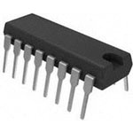
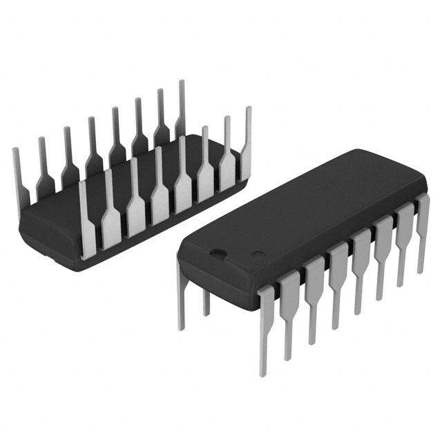
| 产品图片 |
|
| rohs | 符合RoHS无铅 / 符合限制有害物质指令(RoHS)规范要求 |
| 产品系列 | 电源管理 IC,功率因数校正 - PFC,Fairchild Semiconductor FAN4802NY- |
| 数据手册 | |
| 产品型号 | FAN4802NY |
| PCN封装 | |
| 产品目录页面 | |
| 产品种类 | 功率因数校正 - PFC |
| 供应商器件封装 | 16-DIP |
| 包装 | 管件 |
| 单位重量 | 1.628 g |
| 商标 | Fairchild Semiconductor |
| 安装类型 | 通孔 |
| 安装风格 | Through Hole |
| 封装 | Tube |
| 封装/外壳 | 16-DIP(0.300",7.62mm) |
| 封装/箱体 | DIP-16 |
| 工作温度 | -40°C ~ 105°C |
| 工厂包装数量 | 30 |
| 开关频率 | 64 kHz |
| 最大工作温度 | + 105 C |
| 最小工作温度 | - 40 C |
| 标准包装 | 30 |
| 模式 | 平均电流 |
| 电压-电源 | 11 V ~ 22 V |
| 电流-启动 | 30µA |
| 系列 | FAN4802 |
| 频率-开关 | 64kHz |


- 商务部:美国ITC正式对集成电路等产品启动337调查
- 曝三星4nm工艺存在良率问题 高通将骁龙8 Gen1或转产台积电
- 太阳诱电将投资9.5亿元在常州建新厂生产MLCC 预计2023年完工
- 英特尔发布欧洲新工厂建设计划 深化IDM 2.0 战略
- 台积电先进制程称霸业界 有大客户加持明年业绩稳了
- 达到5530亿美元!SIA预计今年全球半导体销售额将创下新高
- 英特尔拟将自动驾驶子公司Mobileye上市 估值或超500亿美元
- 三星加码芯片和SET,合并消费电子和移动部门,撤换高东真等 CEO
- 三星电子宣布重大人事变动 还合并消费电子和移动部门
- 海关总署:前11个月进口集成电路产品价值2.52万亿元 增长14.8%


PDF Datasheet 数据手册内容提取
Is Now Part of To learn more about ON Semiconductor, please visit our website at www.onsemi.com Please note: As part of the Fairchild Semiconductor integration, some of the Fairchild orderable part numbers will need to change in order to meet ON Semiconductor’s system requirements. Since the ON Semiconductor product management systems do not have the ability to manage part nomenclature that utilizes an underscore (_), the underscore (_) in the Fairchild part numbers will be changed to a dash (-). This document may contain device numbers with an underscore (_). Please check the ON Semiconductor website to verify the updated device numbers. The most current and up-to-date ordering information can be found at www.onsemi.com. Please email any questions regarding the system integration to Fairchild_questions@onsemi.com. ON Semiconductor and the ON Semiconductor logo are trademarks of Semiconductor Components Industries, LLC dba ON Semiconductor or its subsidiaries in the United States and/or other countries. ON Semiconductor owns the rights to a number of patents, trademarks, copyrights, trade secrets, and other intellectual property. A listing of ON Semiconductor’s product/patent coverage may be accessed at www.onsemi.com/site/pdf/Patent-Marking.pdf. ON Semiconductor reserves the right to make changes without further notice to any products herein. ON Semiconductor makes no warranty, representation or guarantee regarding the suitability of its products for any particular purpose, nor does ON Semiconductor assume any liability arising out of the application or use of any product or circuit, and specifically disclaims any and all liability, including without limitation special, consequential or incidental damages. Buyer is responsible for its products and applications using ON Semiconductor products, including compliance with all laws, regulations and safety requirements or standards, regardless of any support or applications information provided by ON Semiconductor. “Typical” parameters which may be provided in ON Semiconductor data sheets and/or specifications can and do vary in different applications and actual performance may vary over time. All operating parameters, including “Typicals” must be validated for each customer application by customer’s technical experts. ON Semiconductor does not convey any license under its patent rights nor the rights of others. ON Semiconductor products are not designed, intended, or authorized for use as a critical component in life support systems or any FDA Class 3 medical devices or medical devices with a same or similar classification in a foreign jurisdiction or any devices intended for implantation in the human body. Should Buyer purchase or use ON Semiconductor products for any such unintended or unauthorized application, Buyer shall indemnify and hold ON Semiconductor and its officers, employees, subsidiaries, affiliates, and distributors harmless against all claims, costs, damages, and expenses, and reasonable attorney fees arising out of, directly or indirectly, any claim of personal injury or death associated with such unintended or unauthorized use, even if such claim alleges that ON Semiconductor was negligent regarding the design or manufacture of the part. ON Semiconductor is an Equal Opportunity/Affirmative Action Employer. This literature is subject to all applicable copyright laws and is not for resale in any manner.
F A N 4 8 January 2011 0 0 A / C , FAN4800A/C, FAN4801/02/02L F A N PFC/PWM Controller Combination 4 8 0 1 / 0 2 Features Description /0 2 L Pin-to-Pin Compatible with ML4800 and FAN4800 The highly integrated FAN4800A/C and FAN4801/02/2L — and CM6800 and CM6800A are specially designed for power supplies that consist of boost PFC and PWM. They require very few external P PWM Configurable for Current-Mode or components to achieve versatile protections / F C Feed-forward Voltage-Mode Operation compensation. They are available in 16-pin DIP and / P Internally Synchronized Leading-Edge PFC and SOP packages. W Trailing-Edge PWM in one IC The PWM can be used in either current or voltage M Low Operating Current mode. In voltage mode, feed-forward from the PFC C output bus can reduce the secondary output ripple. o Innovative Switching-Charge Multiplier Divider n Average-Current-Mode for Input-Current Shaping Compared with older productions, ML4800 and tro FAN4800, FAN4800A/C and FAN4801/02/02L have l PFC Over-Voltage and Under-Voltage Protections lower operation current that save power consumption in le r external devices. FAN4800A/C and FAN4801/1S/2/2L PFC Feedback Open-Loop Protection have accurate 49.9% maximum duty of PWM that Co Peak Current Limiting for PFC makes the hold-up time longer. Brownout protection and m PFC soft-start functions are not in ML4800 and b Cycle-by-Cycle Current Limiting for PWM FAN4800. in a Power-On Sequence Control and Soft-Start To evaluate FAN4800A/C, FAN4801/02/2L for replacing ti o Brownout Protection existing FAN4800 and ML4800 boards, five things must n be completed before the fine-tuning procedure: Interleaved PFC/PWM Switching 1. Change R resister from the old value to a higher FAN4801/02/02L Improve Efficiency at Light Load AC resister: between 6M to 8M. f =4•f =4•f for FAN4800A and FAN4801 RTCT PFC PWM 2. Change RT/CT pin from the existing values to f =4•f =2•f for FAN4800C and R =6.8K and C =1000pF to have f =64KHz, RTCT PFC PWM T T PFC FAN4802/02L f =64KHz. PWM 3. VRMS pin needs to be 1.224V at V =85 V for IN AC Applications universal input application from line input from 85V to 270 V . Both poles for the V of AC AC rms Desktop PC Power Supply FAN4801/02/02L don’t need to substantially slower than FAN4800; about 5 to 10 times. Internet Server Power Supply LCD TV, Monitor Power Supply 4. At full load, the average VEA needs to ~4.5V and the ripple on the V needs to be less than 400mV. EA UPS 5. Soft-Start pin, the soft-start current has been Battery Charger reduced to half from the FAN4800 capacitor. DC Motor Power Supply Monitor Power Supply Related Resources Telecom System Power Supply AN-8027 - FAN480X PFC+PWM Combination Distributed Power Controller Application © 2008 Fairchild Semiconductor Corporation www.fairchildsemi.com FAN4800A/C, FAN4801/02/02L • Rev. 1.0.3 1
F A Ordering Information N 4 8 Operating 0 Part Number Package Packing Method 0 Temperature Range A / FAN4800ANY -40°C to +105°C 16-Pin Dual In-Line Package (DIP) Tube C , FAN4800CNY -40°C to +105°C 16-Pin Dual In-Line Package (DIP) Tube F A FAN4800AMY -40°C to +105°C 16-Pin Small Outline Package (SOP) Tape & Reel N 4 FAN4800CMY -40°C to +105°C 16-Pin Small Outline Package (SOP) Tape & Reel 8 0 FAN4801NY -40°C to +105°C 16-Pin Dual In-Line Package (DIP) Tube 1 / 0 FAN4802NY -40°C to +105°C 16-Pin Dual In-Line Package (DIP)) Tube 2 / 0 FAN4802LNY -40°C to +105°C 16-Pin Dual In-Line Package (DIP)) Tube 2 L FAN4801MY -40°C to +105°C 16-Pin Small Outline Package (SOP) Tape & Reel — FAN4802MY -40°C to +105°C 16-Pin Small Outline Package (SOP) Tape & Reel P FAN4802LMY -40°C to +105°C 16-Pin Small Outline Package (SOP) Tape & Reel F C /P W M Part Number PFC:PWM Frequency Ratio Brownout / In Range In / Out C o FAN4800ANY 1:1 1.05V / 1.9V N.A n t FAN4800AMY 1:1 1.05V / 1.9V N.A r o l FAN4800CNY 1:2 1.05V / 1.9V N.A le r FAN4800CMY 1:2 1.05V / 1.9V N.A C o FAN4801NY 1:1 1.05V / 1.9V 1.95V / 2.45V m FAN4802NY 1:2 1.05V / 1.9V 1.95V / 2.45V b i n FAN4802LNY 1:2 0.9V / 1.65V 1.95V / 2.45V a t FAN4801MY 1:1 1.05V / 1.9V 1.95V / 2.45V io n FAN4802MY 1:2 1.05V / 1.9V 1.95V / 2.45V FAN4802LMY 1:2 0.9V / 1.65V 1.95V / 2.45V © 2008 Fairchild Semiconductor Corporation www.fairchildsemi.com FAN4800A/C, FAN4801/02/02L • Rev. 1.0.3 2
F A Application Diagram N 4 8 0 0 A / C , F A N 4 8 0 1 / 0 2 / 0 2 L — P F C / P W M C o n IEA VEA tr o IAC FBPFC ll e ISENSE VREF r VDD C VRMS VDD o m SS OPFC b FBPWM OPWM in a RT/CT GND t i o RAMP ILIMIT n VREF FAN4800A/C FAN4801/02/02L Secondary Figure 1. Typical Application Current Mode © 2008 Fairchild Semiconductor Corporation www.fairchildsemi.com FAN4800A/C, FAN4801/02/02L • Rev. 1.0.3 3
F A Application Diagram N 4 8 0 0 A / C , F A N 4 8 0 1 / 0 2 / 0 2 L — P F C / P W M C o n t r o IEA VEA l l e IAC FBPFC r C ISENSE VREF o VDD m VRMS VDD b SS OPFC i n FBPWM OPWM a t i RT/CT GND o n RAMP ILIMIT VREF FAN4800A/C FAN4801/02/02L VREF Secondary Figure 2. Typical Application Voltage Mode © 2008 Fairchild Semiconductor Corporation www.fairchildsemi.com FAN4800A/C, FAN4801/02/02L • Rev. 1.0.3 4
F A Block Diagram N 4 8 0 0 A / C , F A N 4 8 0 1 / 0 2 / 0 2 L — P F C / P W M C o n t r o l l e r C o m Figure 3. FAN4800A/C Function Block Diagram b i n a t i o n Figure 4. FAN4801/02/02L Function Block Diagram © 2008 Fairchild Semiconductor Corporation www.fairchildsemi.com FAN4800A/C, FAN4801/02/02L • Rev. 1.0.3 5
F A Marking Information N 4 8 0 0 F – Fairchild Logo A / Z – Plant Code C , X – 1-Digit Year Code F A Y – 2-Digit Week Code N TT – 2-Digit Die-Run Code 4 8 0 T – Package Type (M:SOP) 1 / P – Y: Green Package 0 2 M – Manufacture Flow Code /0 2 L — P F C / P W M C o n Figure 5. DIP Top Mark t r o l l e F – Fairchild Logo r C Z – Plant Code o m X – 1-Digit Year Code b Y – 1-Digit Week Code in a TT – 2-Digit Die-Run Code t i o T – Package Type (M:SOP) n P – Y: Green Package M – Manufacture Flow Code Figure 6. SOP Top Mark © 2008 Fairchild Semiconductor Corporation www.fairchildsemi.com FAN4800A/C, FAN4801/02/02L • Rev. 1.0.3 6
F A Pin Configuration N 4 8 0 0 A / C , F A N 4 8 0 1 / 0 2 / 0 2 L — P Figure 7. Pin Configuration (Top View) F C / P Pin Definitions W M Pin # Name Description C o Output of PFC Current Amplifier. The signal from this pin is compared with an internal n 1 IEA t sawtooth to determine the pulse width for PFC gate drive. r o l 2 IAC Input AC Current. For normal operation, this input provides current reference for the multiplier. le The suggested maximum IAC is 100µA. r C PFC Current Sense. The non-inverting input of the PFC current amplifier and the output of o 3 ISENSE multiplier and PFC ILIMIT comparator. m b 4 VRMS Line-Voltage Detection. Line voltage detection. The pin is used for PFC multiplier. i n a PWM Soft-Start. During startup, the SS pin charges an external capacitor with a 10µA constant t i 5 SS current source. The voltage on FBPWM is clamped by SS during startup. In the event of a o n protection condition occurring and/or PWM disabled, the SS pin is quickly discharged. 6 FBPWM PWM Feedback Input. The control input for voltage-loop feedback of PWM stage. 7 RT/CT Oscillator RC Timing Connection. Oscillator timing node; timing set by R and C . T T PWM RAMP Input. In current mode, this pin functions as the current sense input; when in 8 RAMP voltage mode, it is the feed forward sense input from PFC output 380V (feedforward ramp). 9 ILIMIT Peak Current Limit Setting for PWM. The peak current limits setting for PWM. 10 GND Ground. PWM Gate Drive. The totem-pole output drive for PWM MOSFET. This pin is internally 11 OPWM clamped under 15V to protect the MOSFET. PFC Gate Drive. The totem pole output drive for PWM MOSFET. This pin is internally clamped 12 OPFC under 15V to protect the MOSFET. Supply. The power supply pin. The threshold voltages for startup and turn-off are 11V and 13 VDD 9.3V, respectively. The operating current is lower than 10mA. 14 VREF Reference Voltage. Buffered output for the internal 7.5V reference. Voltage Feedback Input for PFC. The feedback input for PFC voltage loop. The inverting input 15 FBPFC of PFC error amplifier. This pin is connected to the PFC output through a divider network. Output of PFC Voltage Amplifier. The error amplifier output for PFC voltage feedback loop. 16 VEA A compensation network is connected between this pin and ground. © 2008 Fairchild Semiconductor Corporation www.fairchildsemi.com FAN4800A/C, FAN4801/02/02L • Rev. 1.0.3 7
F A Absolute Maximum Ratings N 4 Stresses exceeding the absolute maximum ratings may damage the device. The device may not function or be 8 0 operable above the recommended operating conditions and stressing the parts to these levels is not recommended. 0 In addition, extended exposure to stresses above the recommended operating conditions may affect device reliability. A / The absolute maximum ratings are stress ratings only. C , F Symbol Parameter Min. Max. Unit A N VDD DC Supply Voltage 30 V 4 8 VH SS, FBPWM, RAMP, OPWM, OPFC -0.3 30.0 V 0 1 VL IAC, VRMS, RT/CT, ILIMIT, FBPFC, VEA -0.3 7.0 V /0 2 VVREF VREF 7.5 V /0 2 V IEA 0 V +0.3 V IEA VREF L V ISENSE -5.0 0.7 V — N I Input AC Current 1 mA P AC F I VREF Output Current 5 mA C REF / I Peak PFC OUT Current, Source or Sink 0.5 A P PFC-OUT W IPWM-OUT Peak PWM OUT Current, Source or Sink 0.5 A M P Power Dissipation T < 50°C 800 mW C D A o DIP 80.80 °C/W n ΘJA Thermal Resistance (Junction-to-Air) SOP 104.10 °C/W tro l TJ Operating Junction Temperature -40 +125 °C le r TSTG Storage Temperature Range -55 +150 °C C o TL Lead Temperature (Soldering) +260 °C m Human Body Model, b 4.5 kV i JESD22-A114 n ESD Electrostatic Discharge Capability a Charged Device Model, ti 1000 V o JESD22-C101 n Notes: 1. All voltage values, except differential voltage, are given with respect to GND pin. 2. Stresses beyond those listed under Absolute Maximum Ratings may cause permanent damage to the device. Recommended Operating Conditions The Recommended Operating Conditions table defines the conditions for actual device operation. Recommended operating conditions are specified to ensure optimal performance to the datasheet specifications. Fairchild does not recommend exceeding them or designing to Absolute Maximum Ratings. Symbol Parameter Min. Max. Unit T Operating Ambient Temperature -40 +105 °C A © 2008 Fairchild Semiconductor Corporation www.fairchildsemi.com FAN4800A/C, FAN4801/02/02L • Rev. 1.0.3 8
F A Electrical Characteristics N 4 V =15V, T =25°C, R =6.8kΩ, C =1000pF unless noted operating specifications. 8 DD A T T 0 0 Symbol Parameter Conditions Min. Typ. Max. Units A / C VDD Section , F IDD ST Startup Current VDD=VTH-ON-0.1V; OPFC OPWM Open 30 80 µA A N I Operating Current V =13V; OPFC OPWM Open 2.0 2.6 5.0 mA DD-OP DD 4 8 V Turn-On Threshold 10 11 12 V 0 TH-ON Voltage 1 / 0 V Hysteresis 1.5 1.9 V 2 TH / 0 VDD-OVP VDD OVP 27 28 29 V 2 L V V OVP Hysteresis 1 V DD-OVP DD — Oscillator P F f RT/CT Frequency R =6.8kΩ, C =1000pF 240 256 268 kHz OSC-RT/CT T T C PFC & PWM Frequency 60 64 67 /P W fOSC FAN4800C,FAN4802/02L RT=6.8kΩ, CT=1000pF kHz 120 128 134 M PWM Frequency C fDV Voltage Stability 11V ≦ VDD ≦ 22V 2 % o n fDT Temperature Stability -40°C ~ +105°C 2 % tr o Total Variation l fTV (PFC and PWM)(3) Line, Temperature 58 70 kHz le r f Ramp Voltage(3) Valley to Peak 2.8 V C RV o I Discharge Current V =0V, V =2.5V 6.5 15 mA m Discharge RAMP RT/CT b fRANGE Frequency Range(3) 50 75 kHz in t PFC Dead Time R =6.8kΩ, C =1000pF 400 600 800 ns a PFCD T T t i o VREF n V Reference Voltage I =0mA, C =0.1µF 7.4 7.5 7.6 V VREF REF REF Load Regulation of C =0.1µF, I =0mA to 3.5mA V REF REF 30 50 mV VREF1 Reference Voltage V =14V, Rise/Fall Time > 20µs VDD Line Regulation of V C =0.1µF, V =11V to 22V 25 mV VREF2 Reference Voltage REF VDD V Temperature Stability(3) -40°C ~ +105°C 0.4 0.5 % VREF-DT V Total Variation(3) Line, Load, Temperature 7.35 7.65 V VREF-TV V Long-Term Stability(3) T =125°C, 0 ~ 1000HRs 5 25 mV VREF-LS J I . Maximum Current V > 7.35V 5 mA REF-MAX VREF I Output Short Circuit(3) 25 mA OS PFC OVP Comparator V Over-Voltage Protection 2.70 2.75 2.80 V PFC-OVP V PFC OVP Hysteresis 200 250 300 mV PFC-OVP Low-Power Detect Comparator V V Voltage OFF OPFC 0.2 0.3 0.4 V EAOFF EA V OK Comparator IN Voltage Level on FBPFC V to Enable OPWM During 2.3 2.4 2.5 V RD-FBPFC Startup V Hysteresis 1.15 1.25 1.35 V RD-FBPFC © 2008 Fairchild Semiconductor Corporation www.fairchildsemi.com FAN4800A/C, FAN4801/02/02L • Rev. 1.0.3 9
F A Electrical Characteristics (Continued) N 4 V =15V, T =25°C, R =6.8kΩ, C =1000pF unless noted operating specifications. 8 DD A T T 0 0 Symbol Parameter Conditions Min. Typ. Max. Units A / C Voltage Error Amplifier , F FBPFC Input Voltage Range(3) 0 6 V A N V Reference Voltage at T=25°C 2.45 2.50 2.55 V ref 4 AV Open-Loop Gain(3) 35 42 dB 80 1 Gm Transconductance V =V , V =3.75V at T=25°C 50 70 90 µmho / v NONINV INV VEA 0 2 IFBPFC-L Maximum Source Current VFBPFC=2V, VVEA=1.5V 40 50 µA /0 I Maximum Sink Current V =3V, V =6V -50 -40 µA 2 FBPFC-H FBPFC VEA L I Input Bias Current -1 1 µA — BS Output High Voltage on P V 5.8 6 V VEA-H V F VEA C V Output Low Voltage on 0.1 0.4 V /P VEA-L V W VEA M Current Error Amplifier C Input Voltage Range V -1.5 0.7 V o ISENSE (ISENSE Pin)(3) n t GmI Transconductance VNONINV=VINV, VIEA=3.75V 78 88 100 µmho ro l VOFFSET Input Offset Voltage VVEA=0V, IAC Open -10 10 mV le r VIEA-H Output High Voltage 6.8 7.4 8.0 V C o VIEA-L Output Low Voltage 0.1 0.4 V m I Source Current V =-0.6V, V =1.5V 35 50 µA b L ISENSE IEA i n IH Sink Current VISENSE=+0.6V, VIEA=4.0V -50 -35 µA a t A Open-Loop Gain(3) 40 50 dB io I n Tri-Fault Detect V =V to FBPFC OPEN, t Time to FBPFC Open(3) FBPFC PFC-UVP 2 4 ms FBPFC_OPEN 470pF from FBPFC to GND PFC Feedback Under- V 0.4 0.5 0.6 V PFC-UVP Voltage Protection Gain Modulator I Input for AC Current(3) Multiplier Linear Range 0 100 µA AC I =17.67µA, V =1.080V AC RMS 7.50 9.00 10.50 V =2.25V, at T=25°C FBPFC I =20µA, V =1.224V V =2.25V, AC RMS FBPFC 6.30 7.00 7.70 at T=25°C I =25.69µA, V =1.585V GAIN GAIN Modulator(4) AC RMS 3.80 4.20 4.60 V =2.25V, at T=25°C FBPFC I =51.62µA, V =3.169V AC RMS 0.95 1.05 1.16 V =2.25V, at T=25°C FBPFC I =62.23µA, V =3.803V AC RMS 0.66 0.73 0.80 V =2.25V, at T=25°C FBPFC BW Bandwidth(3) I =40µA 2 kHz AC Output Voltage=5.7kΩ × I =20µA, V =1.224V V =2.25V, V AC RMS FBPFC 0.74 0.82 0.90 V o(gm) (I -I )(3) at T=25°C SENSE OFFSET © 2008 Fairchild Semiconductor Corporation www.fairchildsemi.com FAN4800A/C, FAN4801/02/02L • Rev. 1.0.3 10
F A Electrical Characteristics (Continued) N 4 V =15V, T =25°C, R =6.8kΩ, C =1000pF unless noted operating specifications. 8 DD A T T 0 0 Symbol Parameter Conditions Min. Typ. Max. Units A / C PFC ILIMIT Comparator , F Peak Current Limit A V Threshold Voltage, -1.25 -1.15 -1.05 V N PFC-ILIMIT Cycle-by-Cycle Limit 4 8 0 V PFC ILIMIT-Gain Modulator IAC=17.67µA, VRMS=1.08V 200 mV 1 pk Output VFBPFC=2.25V, at T=25°C /0 2 PFC Output Driver / 0 2 V Gate Output Clamping V =22V 13 15 17 V L GATE-CLAMP Voltage DD — V Gate Low Voltage V =15V; I =100mA 1.5 V GATE-L DD O P F V Gate High Voltage V =13V; I =100mA 8 V GATE-H DD O C tr Gate Rising Time VDD=15V; CL=4.7nF; O/P=2V to 9V 40 70 120 ns /P W t Gate Falling Time V =15V; C =4.7nF; O/P=9V to 2V 40 60 110 ns f DD L M D Maximum Duty Cycle V <1.2V 94 97 % PFC-MAX IEA C D Minimum Duty Cycle V >4.5V 0 % o PFC-MIN IEA n Brownout tr o FAN4800A/C, FAN4801/02 1.00 1.05 1.10 V ll V V Threshold Low e RMS-UVL RMS FAN4802L 0.85 0.90 0.95 V r C FAN4800A/C, FAN4801/02 1.85 1.90 1.95 V o V V Threshold High m RMS-UVH RMS FAN4802L 1.60 1.65 1.70 V b i FAN4800A/C, FAN4801/02 750 850 950 mV n V Hysteresis a RMS-UVP FAN4802L 650 750 850 mV ti o n Under-Voltage Protection t 340 410 480 ms UVP Delay Time Soft-Start V Maximum Voltage V =15V 9.5 10.0 10.5 V SS-MAX DD I Soft-Start Current 10 µA SS PWM I Comparator LIMIT V Threshold Voltage 0.95 1.00 1.05 V PWM-ILIMIT t Delay to Output 250 ns PD Leading-Edge Blanking t 170 250 350 ns PWM-Bnk Time Range (FAN4801/02/02L) V RMS AC Voltage Low When V =1.95V at132V 1.90 1.95 2.00 V RMS-L RMS RMS V RMS AC Voltage High When V =2.45V at150V 2.40 2.45 2.50 V RMS-H RMS RMS When V =1.95V at 30% Loading, V VEA Low VEA 1.90 1.95 2.00 V EA-L When V =2.80V at 60% Loading VEA When V =2.45V at 40% Loading, V VEA High VEA 2.40 2.45 2.50 V EA-H When V =3.35V at 70% Loading VEA I Two-Level Current FBPFC Two-Level Current 18 20 22 µA tc © 2008 Fairchild Semiconductor Corporation www.fairchildsemi.com FAN4800A/C, FAN4801/02/02L • Rev. 1.0.3 11
F A Electrical Characteristics (Continued) N 4 V =15V, T =25°C, R =6.8kΩ, C =1000pF unless noted operating specifications. 8 DD A T T 0 0 Symbol Parameter Conditions Min. Typ. Max. Units A / C PWM Output Driver , F VGATE-CLAMP Gate Output Clamping Voltage VDD=22V 13 15 17 V A N V Gate Low Voltage V =15V; I =100mA 1.5 V GATE-L DD O 4 8 VGATE-H Gate High Voltage VDD=13V; IO=100mA 8 V 0 1 t Gate Rising Time V =15V; C =4.7nF 30 60 120 ns / r DD L 0 2 tf Gate Falling Time VDD=15V; CL=4.7nF 30 50 110 ns /0 D Maximum Duty Cycle 49.0 49.5 50.0 % 2 PWM-MAX L V PWM Comparator Level Shift 1.3 1.5 1.8 V — PWM-LS Notes: P 3. This parameter, although guaranteed by design, is not 100% production tested. F C 4. Gain=K × 5.3 × (VRMS2)-1; K=(ISENSE - IOFFSET) × [IAC × (VEA - 0.7V)]-1; VEA(MAX.)=5.6V. /P W M C o n t r o l l e r C o m b i n a t i o n © 2008 Fairchild Semiconductor Corporation www.fairchildsemi.com FAN4800A/C, FAN4801/02/02L • Rev. 1.0.3 12
F A Typical Characteristics N 4 8 0 20.0 2.96 0 18.0 2.94 A / 16.0 2.92 C , 14.0 2.90 F A) 12.0 A) A I(uDD-ST 1068...000 I(uDD-OP 222...888468 N480 1 4.0 2.82 / 0 2.0 2.80 2 / 0.0 2.78 0 -40℃ -25℃ -10℃ 5℃ 20℃ 35℃ 50℃ 65℃ 80℃ 95℃ 110℃125℃ -40℃ -25℃ -10℃ 5℃ 20℃ 35℃ 50℃ 65℃ 80℃ 95℃ 110℃125℃ 2 L — Figure 8. I vs. Temperature Figure 9. I vs. Temperature DD-ST DD-OP P F 11.4 2.0 C / P 11.3 1.9 W 1.8 M 11.2 H-ON (V)11.1 VTH(V) 11..67 Con VT11.0 △ tr 1.5 o l l 10.9 1.4 e r C 10.8 1.3 -40℃ -25℃ -10℃ 5℃ 20℃ 35℃ 50℃ 65℃ 80℃ 95℃ 110℃ 125℃ -40℃ -25℃ -10℃ 5℃ 20℃ 35℃ 50℃ 65℃ 80℃ 95℃ 110℃ 125℃ o m b Figure 10. VTH-ON vs. Temperature Figure 11. VTH vs. Temperature in a t 28.04 65.0 io n 28.02 64.9 28.00 64.8 V(V)DD-OVP22227777....99992468 (kHz)OSC-FAN4801/1S666444...567 F64.4 27.90 27.88 64.3 27.86 64.2 -40℃ -25℃ -10℃ 5℃ 20℃ 35℃ 50℃ 65℃ 80℃ 95℃ 110℃ 125℃ -40℃ -25℃ -10℃ 5℃ 20℃ 35℃ 50℃ 65℃ 80℃ 95℃ 110℃ 125℃ Figure 12. V vs. Temperature Figure 13. f vs. Temperature DD-OVP OSC-FAN4801/1S 130.0 655 129.8 650 129.6 645 Hz) (kOSC-FAN4802/2L 111222999...024 t(ns)PFCD 666334050 F 128.8 625 128.6 620 128.4 615 -40℃ -25℃ -10℃ 5℃ 20℃ 35℃ 50℃ 65℃ 80℃ 95℃ 110℃125℃ -40℃ -25℃ -10℃ 5℃ 20℃ 35℃ 50℃ 65℃ 80℃ 95℃ 110℃125℃ Figure 14. f vs. Temperature Figure 15. t vs. Temperature OSC-FAN4802/2L PFCD © 2008 Fairchild Semiconductor Corporation www.fairchildsemi.com FAN4800A/C, FAN4801/02/02L • Rev. 1.0.3 13
F A Typical Characteristics N 4 8 0 7.520 6 0 A 7.515 5 /C 7.510 , 7.505 V) 4 F V(V)VREF 777...445990050 △V(mVREF1 23 AN480 1 7.485 / 1 0 7.480 2 / 7.475 0 0 -40℃ -25℃ -10℃ 5℃ 20℃ 35℃ 50℃ 65℃ 80℃ 95℃ 110℃125℃ -40℃ -25℃ -10℃ 5℃ 20℃ 35℃ 50℃ 65℃ 80℃ 95℃ 110℃ 125℃ 2 L — Figure 16. V vs. Temperature Figure 17. V vs. Temperature VREF VREF1 P F 0.20 21.5 C 0.18 /P 0.16 21.0 W 0.14 20.5 M △V(mV)VREF2 00000.....0001146802 I.(mA)REF-MAX 112990...050 Contro l 0.02 18.5 le 0.00 r C -0.02 18.0 o -40℃ -25℃ -10℃ 5℃ 20℃ 35℃ 50℃ 65℃ 80℃ 95℃ 110℃125℃ -40℃ -25℃ -10℃ 5℃ 20℃ 35℃ 50℃ 65℃ 80℃ 95℃ 110℃125℃ m b Figure 18. VVREF2 vs. Temperature Figure 19. IREF-MAX. vs. Temperature in a t i 2.742 252.2 o n 2.740 252.0 2.738 V) 251.8 V) m V(PFC-OVP 22..773346 △V(PFC-OVP 225511..46 251.2 2.732 251.0 2.730 250.8 -40℃ -25℃ -10℃ 5℃ 20℃ 35℃ 50℃ 65℃ 80℃ 95℃ 110℃125℃ -40℃ -25℃ -10℃ 5℃ 20℃ 35℃ 50℃ 65℃ 80℃ 95℃ 110℃125℃ Figure 20. V vs. Temperature Figure 21. V vs. Temperature PFC-OVP PFC-OVP 2.400 1.275 2.398 1.270 1.265 V(V)RD-FBPFC 222...333999246 △V(V)RD-FBPFC 11..225650 1.250 2.390 1.245 2.388 1.240 -40℃ -25℃ -10℃ 5℃ 20℃ 35℃ 50℃ 65℃ 80℃ 95℃ 110℃125℃ -40℃ -25℃ -10℃ 5℃ 20℃ 35℃ 50℃ 65℃ 80℃ 95℃ 110℃125℃ Figure 22. V vs. Temperature Figure 23. V vs. Temperature RD-FBPFC RD-FBPFC © 2008 Fairchild Semiconductor Corporation www.fairchildsemi.com FAN4800A/C, FAN4801/02/02L • Rev. 1.0.3 14
F A Typical Characteristics N 4 8 0 2.502 74 0 A 2.500 / 73 C 2.498 , F V(V)ref 22..449946 Gm(umho)v 7723 AN48 0 2.492 1 2.490 72 /0 2 / 2.488 71 0 -40℃ -25℃ -10℃ 5℃ 20℃ 35℃ 50℃ 65℃ 80℃ 95℃ 110℃125℃ -40℃ -25℃ -10℃ 5℃ 20℃ 35℃ 50℃ 65℃ 80℃ 95℃ 110℃ 125℃ 2 L — Figure 24. V vs. Temperature Figure 25. Gm vs. Temperature ref V P F 4.5 94 C / 4.0 92 P W 3.5 90 M V(mV)OFFSET 1223....5050 Gm(umho)I 888468 Contr o 1.0 82 ll e 0.5 80 r 0.0 78 C -40℃ -25℃ -10℃ 5℃ 20℃ 35℃ 50℃ 65℃ 80℃ 95℃ 110℃125℃ -40℃ -25℃ -10℃ 5℃ 20℃ 35℃ 50℃ 65℃ 80℃ 95℃ 110℃125℃ o m b Figure 26. V vs. Temperature Figure 27. Gm vs. Temperature OFFSET I in a t 7.10 6.1 io n 7.05 6.0 7.00 5.9 2 6.95 Ω) 5.8 N k AI 6.90 ul( G m 5.7 6.85 R 5.6 6.80 6.75 5.5 6.70 5.4 -40℃ -25℃ -10℃ 5℃ 20℃ 35℃ 50℃ 65℃ 80℃ 95℃ 110℃125℃ -40℃ -25℃ -10℃ 5℃ 20℃ 35℃ 50℃ 65℃ 80℃ 95℃ 110℃125℃ Figure 28. GAIN2 vs. Temperature Figure 29. Rmul vs. Temperature -1.1775 295 -1.1780 290 -1.1785 285 -1.1790 280 V)-1.1795 V) V(PFC-ILIMIT--11..11880050 △V(mpk 222677505 -1.1810 -1.1815 260 -1.1820 255 -1.1825 250 -40℃ -25℃ -10℃ 5℃ 20℃ 35℃ 50℃ 65℃ 80℃ 95℃ 110℃125℃ -40℃ -25℃ -10℃ 5℃ 20℃ 35℃ 50℃ 65℃ 80℃ 95℃ 110℃125℃ Figure 30. V vs. Temperature Figure 31. V vs. Temperature PFC-ILIMIT pk © 2008 Fairchild Semiconductor Corporation www.fairchildsemi.com FAN4800A/C, FAN4801/02/02L • Rev. 1.0.3 15
F A Typical Characteristics N 4 8 0 1.010 10.1 0 1.009 10.0 A / 9.9 C 1.008 , 9.8 V(V)PWM-ILIMIT 111...000000567 I(uA)SS 9999....4567 FAN480 1.004 1 9.3 / 0 1.003 9.2 2 / 1.002 9.1 0 -40℃ -25℃ -10℃ 5℃ 20℃ 35℃ 50℃ 65℃ 80℃ 95℃ 110℃125℃ -40℃ -25℃ -10℃ 5℃ 20℃ 35℃ 50℃ 65℃ 80℃ 95℃ 110℃125℃ 2 L — Figure 32. V vs. Temperature Figure 33. I vs. Temperature PWM-ILIMIT SS P F 1.048 867.5 C 1.047 867.0 /P 1.046 866.5 W 1.045 V) 866.0 M V(V)RMS-UVP 1111....000044441234 △V(mRMS-UVP 888886666634455.....50505 Contro l 1.040 863.0 le 1.039 862.5 r C 1.038 862.0 -40℃ -25℃ -10℃ 5℃ 20℃ 35℃ 50℃ 65℃ 80℃ 95℃ 110℃125℃ -40℃ -25℃ -10℃ 5℃ 20℃ 35℃ 50℃ 65℃ 80℃ 95℃ 110℃125℃ o m b Figure 34. VRMS-UVP vs. Temperature Figure 35. VRMS-UVP vs. Temperature in a 1.940 2.446 ti o 1.939 2.445 n 1.938 2.444 2.443 1.937 V(V)RMS-L 11..993356 (V)RMS-H 222...444444012 1.934 V 2.439 1.933 2.438 1.932 2.437 1.931 2.436 -40℃ -25℃ -10℃ 5℃ 20℃ 35℃ 50℃ 65℃ 80℃ 95℃ 110℃125℃ 2.435 -40℃ -25℃ -10℃ 5℃ 20℃ 35℃ 50℃ 65℃ 80℃ 95℃ 110℃125℃ Figure 36. V vs. Temperature Figure 37. V vs. Temperature RMS-L RMS-H 1.942 2.436 1.940 2.434 1.938 2.432 V(V)EA-L 11..993346 V(V)EA-H 22..442380 1.932 2.426 1.930 2.424 1.928 -40℃-25℃ -10℃ 5℃ 20℃ 35℃ 50℃ 65℃ 80℃ 95℃ 110 125 -40℃ -25℃ -10℃ 5℃ 20℃ 35℃ 50℃ 65℃ 80℃ 95℃ 110℃125℃ ℃ ℃ Figure 38. V vs. Temperature Figure 39. V vs. Temperature EA-L EA-H © 2008 Fairchild Semiconductor Corporation www.fairchildsemi.com FAN4800A/C, FAN4801/02/02L • Rev. 1.0.3 16
F A Typical Characteristics N 4 8 0 14.7 14.4 0 A 14.6 14.3 / C (V)ATE-CLAMP-PFC 11114444....2345 (V)E-CLAMP-PWM 11113444....9012 , FAN48 VG 14.1 GAT 0 V 13.8 1 14.0 /0 13.9 13.7 2 / -40℃ -25℃ -10℃ 5℃ 20℃ 35℃ 50℃ 65℃ 80℃ 95℃ 110℃125℃ 13.6 0 -40℃ -25℃ -10℃ 5℃ 20℃ 35℃ 50℃ 65℃ 80℃ 95℃ 110℃125℃ 2 L — Figure 40. V vs. Temperature Figure 41. V vs. Temperature GATE-CLAMP-PFC GATE-CLAMP-PWM P F 96.06 49.80 C / 96.04 P 49.75 W 96.02 96.00 %)49.70 M (%)C-MAX 9955..9968 (WM-MAX49.65 Con DPF 95.94 DP49.60 tr o 95.92 49.55 ll e 95.90 r 49.50 C 95.88 -40℃ -25℃ -10℃ 5℃ 20℃ 35℃ 50℃ 65℃ 80℃ 95℃ 110 125 -40℃ -25℃ -10℃ 5℃ 20℃ 35℃ 50℃ 65℃ 80℃ 95℃ 110℃125℃ ℃ ℃ o m b Figure 42. D vs. Temperature Figure 43. D vs. Temperature PFC-MAX PWM-MAX in a t 21.0 1.460 io n 20.8 1.455 20.6 1.450 20.4 V) I(uA)tc 2200..02 V(PWM-LS 1.445 1.440 19.8 1.435 19.6 19.4 1.430 -40℃ -25℃ -10℃ 5℃ 20℃ 35℃ 50℃ 65℃ 80℃ 95℃ 110℃125℃ -40℃ -25℃ -10℃ 5℃ 20℃ 35℃ 50℃ 65℃ 80℃ 95℃ 110℃125℃ Figure 44. I vs. Temperature Figure 45. V vs. Temperature tc PWM-LS © 2008 Fairchild Semiconductor Corporation www.fairchildsemi.com FAN4800A/C, FAN4801/02/02L • Rev. 1.0.3 17
F A Functional Description N 4 The FAN4800A/C and FAN4801/02/02L consist of an IAC(VEA0.7) 8 average current controlled, continuous boost Power IGAINMOD VRMS2 K (1) 00 Factor Correction (PFC) front-end and a synchronized A / Pulse Width Modulator (PWM) back-end. The PWM can C be used in current or voltage mode. In voltage mode, Note that the output current of the gain modulator is , F feed forward from the PFC output bus can be used to limited around 159μA and the maximum output voltage A improve the line regulation of PWM. In either mode, the of the gain modulator is limited to 159μA x 5.7K=0.906V. N PWM stage uses conventional trailing-edge, duty-cycle This 0.906V also determines the maximum input power. 4 8 modulation. This propriety leading/trailing edge 0 modulation results in a higher usable PFC error However, IGAINMOD cannot be measured directly from 1 amplifier bandwidth and can significantly reduce the ISENSE. ISENSE=IGAINMOD – IOFFSET and IOFFSET can only /0 2 size of the PFC DC bus capacitor. bise 0 mA.e Tayspuirceadl IwOhFeFSnE VT EisA a irso ulensds 3 t1hμaAn ~0 .458Vμ aAn. d IGAINMOD /02 The synchronization of the PWM with the PFC simplifies L the PWM compensation due to the controlled ripple on Selecting R for IAC Pin — the PFC output capacitor (the PWM input capacitor). AC The PWM section of the FAN4800A, FAN4801/1S The IAC pin is the input of the gain modulator and also PF operates at the same frequency as the PFC; and a current mirror input and requires current input. C FAN4800C, FAN4802/2L operates at double with PFC. Selecting a proper resistor RAC provides a good sine /P wave current derived from the line voltage and helps W In addition to power factor correction, a number of program the maximum input power and minimum input M protection features are built into this series. They line voltage. RAC=VIN peak x 56KΩ. For example, if the C include soft-start, PFC over-voltage protection, peak minimum line voltage is 75VAC, the RAC=75 x 1.414 x o current limiting, brownout protection, duty cycle limiting, 56KΩ=6MΩ. n and under-voltage lockout (UVLO). t r o Current Amplifier Error, IEA l l Gain Modulator e The current error amplifier’s output controls the PFC r The gain modulator is the heart of the PFC, as the duty cycle to keep the average current through the C o circuit block controls the response of the current loop to boost inductor a linear function of the line voltage. At m line voltage waveform and frequency, RMS line voltage, the inverting input to the current error amplifier, the b and PFC output voltages. There are three inputs to the output current of the gain modulator is summed with a in gain modulator: current, which results in a negative voltage being a t impressed upon the ISENSE pin. i 1. A current representing the instantaneous input o n voltage (amplitude and wave shape) to the PFC. The The negative voltage on ISENSE represents the sum of rectified AC input sine wave is converted to a all currents flowing in the PFC circuit and is typically proportional current via a resistor and is fed into the derived from a current sense resistor in series with the gain modulator at IAC. Sampling current in this way negative terminal of the input bridge rectifier. minimizes ground noise, required in high-power, switching-power conversion environments. The gain The inverting input of the current error amplifier is a modulator responds linearly to this current. virtual ground. Given this fact, and the arrangement of the duty cycle modulator polarities internal to the PFC, 2. A voltage proportional to the long-term RMS AC line an increase in positive current from the gain modulator voltage, derived from the rectified line voltage after causes the output stage to increase its duty cycle until scaling and filtering. This signal is presented to the the voltage on ISENSE is adequately negative to cancel gain modulator at VRMS. The output of the gain this increased current. Similarly, if the gain modulator’s modulator is inversely proportional to VRMS (except output decreases, the output duty cycle decreases to at unusually low values of VRMS, where special gain achieve a less negative voltage on the ISENSE pin. contouring takes over to limit power dissipation of the circuit components under brownout conditions). PFC Cycle-By-Cycle Current Limiter 3. The output of the voltage error amplifier, VEA. The As well as being a part of the current feedback loop, the gain modulator responds linearly to variations in this ISENSE pin is a direct input to the cycle-by-cycle voltage. current limiter for the PFC section. If the input voltage at The output of the gain modulator is a current signal, in this pin is less than -1.15V, the output of the PFC is the form of a full wave rectified sinusoid at twice the line disabled until the protection flip-flop is reset by the clock frequency. This current is applied to the virtual ground pulse at the start of the next PFC power cycle. (negative) input of the current error amplifier. In this way, the gain modulator forms the reference for the current error loop and ultimately controls the instantaneous current draw of the PFC from the power line. The general form of the output of the gain modulator is: © 2008 Fairchild Semiconductor Corporation www.fairchildsemi.com FAN4800A/C, FAN4801/02/02L • Rev. 1.0.3 18
F TriFault Detect™ Error Amplifier Compensation A N To improve power supply reliability, reduce system The PWM loading of the PFC can be modeled as a 4 component count, and simplify compliance to UL 1950 negative resistor because an increase in the input 8 0 safety standards, the FAN4800A/C, FAN4801/02/02L voltage to the PWM causes a decrease in the input 0 includes TriFault Detect. This feature monitors FBPFC current. This response dictates the proper A / for certain PFC fault conditions. compensation of the two transconductance error C amplifiers. Figure 46 shows the types of compensation , In a feedback path failure, the output of the PFC could F networks most commonly used for the voltage and A exceed safe operating limits. With such a failure, current error amplifiers, along with their respective N FBPFC exceeds its normal operating area. Should return points. The current-loop compensation is 4 FBPFC go too LOW, too HIGH, or OPEN, TriFault 8 returned to VREF to produce a soft-start characteristic 0 Detect senses the error and terminates the PFC output on the PFC: As the reference voltage increases from 1 drive. /0 0V, it creates a differentiated voltage on IEA, which 2 TriFault detect is an entirely internal circuit. It requires prevents the PFC from immediately demanding a full /0 no external components to serve its protective function. duty cycle on its boost converter. Complete design is 2 L referred in application note AN-6078SC. — PFC Over-Voltage Protection There is an RC filter between RSENSE and ISENSE pin. P In the FAN4800A/C, FAN4801/02/02L, the PFC OVP There are two reasons to add a filter at the ISENSE pin: F C comparator serves to protect the power circuit from 1. Protection: During startup or inrush current / being subjected to excessive voltages if the load P conditions, there is a large voltage across R , SENSE W changes suddenly. A resistor divider from the high- which is the sensing resistor of the PFC boost M voltage DC output of the PFC is fed to FBPFC. When converter. It requires the ISENSE filter to attenuate the voltage on FBPFC exceeds 2.75V, the PFC output C the energy. driver is shut down. The PWM section continues to o n operate. The OVP comparator has 250mV of hysteresis 2. To reduce L, the boost inductor: The ISENSE filter t and the PFC does not restart until the voltage at FBPFC also can reduce the boost inductor value since the ro drops below 2.50V. VDD OVP can also serve as a ISENSE filter behaves like an integrator before the lle redundant PFC OVP protection. V OVP threshold is ISENSE pin, which is the input of the current error r DD 28V with 1V hysteresis. amplifier, IEA. C o The ISENSE filter is an RC filter. The resistor value of m Selecting PFC RSENSE the ISENSE filter is between 100Ω and 50Ω because b i RSENSE is the sensing resistor of the PFC boost IOFFSET x RFILTER can generate a negative offset voltage na converter. During the steady state, line input current x of IEA. Selecting an RFILTER equal to 50Ω keeps the t R equals I x 5.7KΩ. offset of the IEA less than 3mV. Design the pole of io SENSE GAINMOD ISENSE filter at f /6, one sixth of the PFC switching n PFC At full load, the average VEA needs to around 4.5V and frequency, so the boost inductor can be reduced six ripple on the VEA needs to be less than 400mV. times without disturbing the stability. The capacitor of Choose the resistance of the sensing resistor: the ISENSE filter, C , is approximately 100nF. FILTER 4.50.75.7KIACGainV 2 R IN (2) sense 25.60.7Line input Power where 5.6 is V maximum output. EA PFC Soft-Start PFC startup is controlled by V level. Before FBPFC EA voltage reaches 2.4V, the V level is around 2.8V. At EA 90V , the PFC soft-start time is 90ms. AC PFC Brownout The AC UVP comparator monitors the AC input voltage. The FAN4800A/C, FAN4801/02 disables PFC as lower AC input such that the VRMS is less than 1.05V. The brownout voltage of FAN4802L is lower than FAN4801/1S/2, such that the VRMS is less than 0.9V. Figure 46. Compensation Network Connection for the Voltage and Current Error Amplifiers © 2008 Fairchild Semiconductor Corporation www.fairchildsemi.com FAN4800A/C, FAN4801/02/02L • Rev. 1.0.3 19
F Two-Level PFC Function Pulse Width Modulator (PWM) A N To improve the efficiency, the system can reduce PFC The operation of the PWM section is straightforward, 4 switching loss at low line and light load by reducing the but there are several points that should be noted. 8 0 PFC output voltage. The two-level PFC output of Foremost among these is the inherent synchronization 0 FAN4801/02/02L can be programmable. of PWM with the PFC section of the device, from which A / it also derives its basic timing. The PWM is capable of C As Figure 47 shows, FAN4801/02/02L detect VEA pin current-mode or voltage-mode operation. In current- , and VRMS pin to determine the system operates low F mode applications, the PWM ramp (RAMP) is usually A line and light load or not. At the second-level PFC, there derived directly from a current sensing resistor or N is a current of 20µA through RF2 from FBPFC pin. So current transformer in the primary of the output stage. It 4 the second-level PFC output voltage can be calculated 8 is thereby representative of the current flowing in the 0 as. converter’s output stage. I , which provides cycle-by- 1 LIMIT / 0 R R cycle current limiting, is typically connected to RAMP in 2 Output F1R F2(2.5V 20uARF2) (3) such applications. For voltage-mode operation and /0 F2 certain specialized applications, RAMP can be 2 For example, if the second-level PFC output voltage is connected to a separate RC timing network to generate L expected as 300V and normal voltage is 387V, a voltage ramp against which FBPWM is compared. — according to the equation, RF2 is 28kΩ RF1 is 4.3MΩ. Under these conditions, the use of voltage feed-forward P from the PFC bus can assist in line regulation accuracy F The programmable range of second level PFC output C and response. As in current-mode operation, the I voltage is 340V ~ 300V. LIMIT / P input is used for output stage over-current protection. W No voltage error amplifier is included in the PWM stage, M as this function is generally performed on the output side of the PWM’s isolation boundary. To facilitate the C o design of opto-coupler feedback circuitry, an offset has n been built into the PWM’s RAMP input that allows t r FBPWM to command a 0% duty cycle for input voltages o l below typical 1.5V. le r C PWM Cycle-By-Cycle Current Limiter o m The ILIMIT pin is a direct input to the cycle-by-cycle b current limiter for the PWM section. Should the input i n voltage at this pin ever exceed 1V, the output flip-flop is a reset by the clock pulse at the start of the next PWM t i o Figure 47. Two-Level PFC Scheme power cycle. When the ILIMIT triggers the cycle-by-cycle n bi-cycle current, it limits the PWM duty cycle mode and the power dissipation is reduced during the dead-short Oscillator (R /C ) T T condition. The oscillator frequency is determined by the values of R and C , which determine the ramp and off-time of T T V OK Comparator the oscillator output clock: IN The V OK comparator monitors the DC output of the IN 1 PFC and inhibits the PWM if the voltage on FBPFC is fRT/CT t t (4) less than its nominal 2.4V. Once the voltage reaches RT/CT DEAD 2.4V, which corresponds to the PFC output capacitor The dead time of the oscillator is derived from the being charged to its rated boost voltage, the soft-start following equation: begins. VREF1 tRT/CT CT RT lnVREF3.8 (5) PWM Soft-Start (SS) at V =7.5V and t =CT x RT x 0.56. REF RT/CT PWM startup is controlled by selection of the external The dead time of the oscillator is determined using: capacitor at soft-start. A current source of 10µA supplies the charging current for the capacitor and 2.8V t C 360C (6) startup of the PWM begins at 1.5V. DEAD T T 7.78mA The dead time is so small (t >>t ) that the RT/CT DEAD operating frequency can typically be approximated by: 1 fRT/CT (7) t RT/CT © 2008 Fairchild Semiconductor Corporation www.fairchildsemi.com FAN4800A/C, FAN4801/02/02L • Rev. 1.0.3 20
F PWM Control (RAMP) Leading/Trailing Modulation A N When the PWM section is used in current mode, RAMP Conventional PWM techniques employ trailing-edge 4 is generally used as the sampling point for a voltage, modulation, in which the switch turns on right after the 8 0 representing the current in the primary of the PWM’s trailing edge of the system clock. The error amplifier 0 output transformer. The voltage is derived either from a output is then compared with the modulating ramp up. A / current sensing resistor or a current transformer. In The effective duty cycle of the trailing edge modulation C voltage mode, RAMP is the input for a ramp voltage is determined during the on-time of the switch. , F generated by a second set of timing components (RRAMP, In the case of leading-edge modulation, the switch is A C ) that have a minimum value of 0V and a peak N vaRlAuMeP of approximately 6V. In voltage mode, feed turned off exactly at the leading edge of the system 4 clock. When the modulating ramp reaches the level of 8 forward from the PFC output bus is an excellent way to 0 derive the timing ramp for the PWM stage. the error amplifier output voltage, the switch is turned 1 on. The effective duty-cycle of the leading-edge /0 modulation is determined during off-time of the switch. 2 Generating V /0 DD 2 After turning on the FAN4800A/C, FAN4801/02/02L at L 11V, the operating voltage can vary from 9.3V to 28V. — The threshold voltage of the V OVP comparator is DD P 28V and its hysteresis is 1V. When VDD reaches 28V, F OPFC is LOW, and the PWM section is not disturbed. C / There are two ways to generate V : use auxiliary P DD power supply around 15V or use bootstrap winding to W self-bias the FAN4800A/C, FAN4801/02/02L system. M The bootstrap winding can be taped from the PFC boost C choke or the transformer of the DC-to-DC stage. o n t r o l l e r C o m b i n a t i o n © 2008 Fairchild Semiconductor Corporation www.fairchildsemi.com FAN4800A/C, FAN4801/02/02L • Rev. 1.0.3 21
F A Physical Dimensions N 4 8 0 0 A / A C 19.68 , F 18.66 A 16 9 N 4 8 0 1 / 6.60 0 2 6.09 /0 2 L — 1 8 P F (0.40) C TOP VIEW /P W M C 0.38 MIN 8.13 o n 5.33 MAX 7.62 t r o 3.42 ll e 3.17 r C o 3.81 m 2.92 b 15 in 2.54 0.58 0.35 0 at A 0.20 io 0.35 n 1.78 1.14 8.69 17.78 SIDE VIEW NOTES: UNLESS OTHERWISE SPECIFIED A THIS PACKAGE CONFORMS TO JEDEC MS-001 VARIATION BB B) ALL DIMENSIONS ARE IN MILLIMETERS. C) DIMENSIONS ARE EXCLUSIVE OF BURRS, MOLD FLASH, AND TIE BAR PROTRUSIONS D) CONFORMS TO ASME Y14.5M-1994 E) DRAWING FILE NAME: N16EREV1 Figure 48. 16-Pin Dual In-Line Package (DIP) Package drawings are provided as a service to customers considering Fairchild components. Drawings may change in any manner without notice. Please note the revision and/or date on the drawing and contact a Fairchild Semiconductor representative to verify or obtain the most recent revision. Package specifications do not expand the terms of Fairchild’s worldwide terms and conditions, specifically the warranty therein, which covers Fairchild products. Always visit Fairchild Semiconductor’s online packaging area for the most recent package drawings: http://www.fairchildsemi.com/packaging/. © 2008 Fairchild Semiconductor Corporation www.fairchildsemi.com FAN4800A/C, FAN4801/02/02L • Rev. 1.0.3 22
F A Physical Dimensions (Continued) N 4 8 0 0 A / C , F A N 4 8 0 1 / 0 2 / 0 2 L — P F C / P W M C o n t r o l l e r C o m b i n a t i o n Figure 49. 16-Pin Small Outline Package (SOIC) Package drawings are provided as a service to customers considering Fairchild components. Drawings may change in any manner without notice. Please note the revision and/or date on the drawing and contact a Fairchild Semiconductor representative to verify or obtain the most recent revision. Package specifications do not expand the terms of Fairchild’s worldwide terms and conditions, specifically the warranty therein, which covers Fairchild products. Always visit Fairchild Semiconductor’s online packaging area for the most recent package drawings: http://www.fairchildsemi.com/packaging/. © 2008 Fairchild Semiconductor Corporation www.fairchildsemi.com FAN4800A/C, FAN4801/02/02L • Rev. 1.0.3 23
F A N 4 8 0 0 A / C , F A N 4 8 0 1 / 0 2 / 0 2 L — P F C / P W M C o n t r o l l e r C o m b i n a t i o n © 2008 Fairchild Semiconductor Corporation www.fairchildsemi.com FAN4800A/C, FAN4801/02/02L • Rev. 1.0.3 24
ON Semiconductor and are trademarks of Semiconductor Components Industries, LLC dba ON Semiconductor or its subsidiaries in the United States and/or other countries. ON Semiconductor owns the rights to a number of patents, trademarks, copyrights, trade secrets, and other intellectual property. A listing of ON Semiconductor’s product/patent coverage may be accessed at www.onsemi.com/site/pdf/Patent−Marking.pdf. ON Semiconductor reserves the right to make changes without further notice to any products herein. ON Semiconductor makes no warranty, representation or guarantee regarding the suitability of its products for any particular purpose, nor does ON Semiconductor assume any liability arising out of the application or use of any product or circuit, and specifically disclaims any and all liability, including without limitation special, consequential or incidental damages. Buyer is responsible for its products and applications using ON Semiconductor products, including compliance with all laws, regulations and safety requirements or standards, regardless of any support or applications information provided by ON Semiconductor. “Typical” parameters which may be provided in ON Semiconductor data sheets and/or specifications can and do vary in different applications and actual performance may vary over time. All operating parameters, including “Typicals” must be validated for each customer application by customer’s technical experts. ON Semiconductor does not convey any license under its patent rights nor the rights of others. ON Semiconductor products are not designed, intended, or authorized for use as a critical component in life support systems or any FDA Class 3 medical devices or medical devices with a same or similar classification in a foreign jurisdiction or any devices intended for implantation in the human body. Should Buyer purchase or use ON Semiconductor products for any such unintended or unauthorized application, Buyer shall indemnify and hold ON Semiconductor and its officers, employees, subsidiaries, affiliates, and distributors harmless against all claims, costs, damages, and expenses, and reasonable attorney fees arising out of, directly or indirectly, any claim of personal injury or death associated with such unintended or unauthorized use, even if such claim alleges that ON Semiconductor was negligent regarding the design or manufacture of the part. ON Semiconductor is an Equal Opportunity/Affirmative Action Employer. This literature is subject to all applicable copyright laws and is not for resale in any manner. PUBLICATION ORDERING INFORMATION LITERATURE FULFILLMENT: N. American Technical Support: 800−282−9855 Toll Free ON Semiconductor Website: www.onsemi.com Literature Distribution Center for ON Semiconductor USA/Canada 19521 E. 32nd Pkwy, Aurora, Colorado 80011 USA Europe, Middle East and Africa Technical Support: Order Literature: http://www.onsemi.com/orderlit Phone: 303−675−2175 or 800−344−3860 Toll Free USA/Canada Phone: 421 33 790 2910 Fax: 303−675−2176 or 800−344−3867 Toll Free USA/Canada Japan Customer Focus Center For additional information, please contact your local Email: orderlit@onsemi.com Phone: 81−3−5817−1050 Sales Representative © Semiconductor Components Industries, LLC www.onsemi.com www.onsemi.com 1
Mouser Electronics Authorized Distributor Click to View Pricing, Inventory, Delivery & Lifecycle Information: O N Semiconductor: FAN4802NY FAN4802MY