 Datasheet下载
- 型号: PESD5V0V1BCSF,315
- 制造商: NXP Semiconductors
- 库位|库存: xxxx|xxxx
- 要求:
| 数量阶梯 | 香港交货 | 国内含税 |
| +xxxx | $xxxx | ¥xxxx |
查看当月历史价格
查看今年历史价格
PESD5V0V1BCSF,315产品简介:
ICGOO电子元器件商城为您提供PESD5V0V1BCSF,315由NXP Semiconductors设计生产,在icgoo商城现货销售,并且可以通过原厂、代理商等渠道进行代购。 PESD5V0V1BCSF,315价格参考。NXP SemiconductorsPESD5V0V1BCSF,315封装/规格:TVS - 二极管, 12.8V Clamp 1A (8/20µs) Ipp Tvs Diode Surface Mount DSN0603-2。您可以下载PESD5V0V1BCSF,315参考资料、Datasheet数据手册功能说明书,资料中有PESD5V0V1BCSF,315 详细功能的应用电路图电压和使用方法及教程。
Nexperia USA Inc. 的 PESD5V0V1BCSF,315 是一款瞬态电压抑制(TVS)二极管,专为保护敏感电子元件免受静电放电(ESD)、浪涌脉冲和其他瞬态过压事件的损害而设计。该器件具有低工作电压(标称5V)、快速响应时间和低钳位电压,适用于对信号完整性要求较高的应用场景。

主要应用场景包括:

1. 便携式电子设备:广泛用于智能手机、平板电脑和可穿戴设备中,保护USB接口(如USB 2.0和USB Type-C)、HDMI端口、音频插孔等高速数据线路免受ESD冲击。

2. 通信接口保护:适用于I²C、I³C、UART、SPI等低电压数字信号线路的防护,确保系统在恶劣电磁环境下的稳定运行。

3. 消费类电子产品:用于电视、机顶盒、数码相机等设备中的敏感电路保护,提升产品可靠性与使用寿命。

4. 工业与汽车电子:适用于车载信息娱乐系统、传感器接口和小型控制模块中的信号线保护,符合AEC-Q101车规认证,具备良好的温度稳定性和耐久性。

PESD5V0V1BCSF,315 采用小型化DFN1006-2封装,节省PCB空间,适合高密度布局的现代电子产品。其低电容特性(典型值<1pF)确保对高速信号传输影响极小,是高频、低功耗应用的理想选择。
| 参数 | 数值 |
| 产品目录 | |
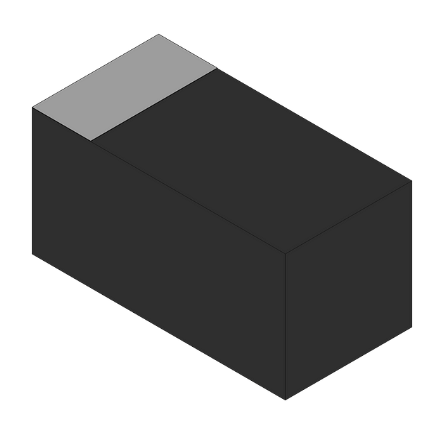
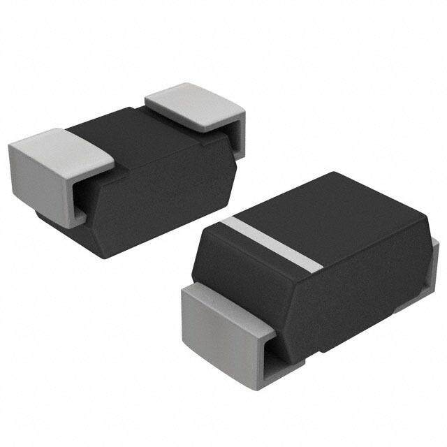
| 描述 | TVS DIODE 5VWM 12.8VC SOD962TVS 二极管 - 瞬态电压抑制器 BIDIRECT ESD 5V |
| 产品分类 | |
| 品牌 | NXP Semiconductors |
| 产品手册 | |
| 产品图片 |
|
| rohs | 符合RoHS无铅 / 符合限制有害物质指令(RoHS)规范要求 |
| 产品系列 | 二极管与整流器,TVS二极管,TVS 二极管 - 瞬态电压抑制器,NXP Semiconductors PESD5V0V1BCSF,315- |
| mouser_ship_limit | 该产品可能需要其他文件才能进口到中国。 |
| 数据手册 | |
| 产品型号 | PESD5V0V1BCSF,315 |
| PCN封装 | |
| 不同频率时的电容 | 5.3pF @ 1MHz |
| 产品种类 | TVS 二极管 - 瞬态电压抑制器 |
| 供应商器件封装 | 2-DSN(0.60x0.30) |
| 其它名称 | 568-10746-1 |
| 击穿电压 | 10 V |
| 功率-峰值脉冲 | 8W |
| 包装 | 剪切带 (CT) |
| 单向通道 | - |
| 双向通道 | 1 |
| 商标 | NXP Semiconductors |
| 安装类型 | 表面贴装 |
| 安装风格 | SMD/SMT |
| 封装 | Reel |
| 封装/外壳 | 2-XFDFN |
| 封装/箱体 | DSN-0603-2 |
| 尺寸 | 0.3 mm W x 0.6 mm L x 0.3 mm H |
| 峰值浪涌电流 | 1 A |
| 峰值脉冲功率耗散 | 8 W |
| 工作温度 | -55°C ~ 150°C (TA) |
| 工厂包装数量 | 9000 |
| 应用 | 通用 |
| 最大工作温度 | + 150 C |
| 最小工作温度 | - 55 C |
| 极性 | Bidirectional |
| 标准包装 | 1 |
| 电压-击穿(最小值) | 6V |
| 电压-反向关态(典型值) | 5V(最小值) |
| 电压-箝位(最大值)@Ipp | 12.8V |
| 电容 | 4.3 pF |
| 电流-峰值脉冲(10/1000µs) | 1A (8/20µs) |
| 电源线路保护 | 无 |
| 端接类型 | SMD/SMT |
| 类型 | 齐纳 |
| 钳位电压 | 12.8 V |


- 商务部:美国ITC正式对集成电路等产品启动337调查
- 曝三星4nm工艺存在良率问题 高通将骁龙8 Gen1或转产台积电
- 太阳诱电将投资9.5亿元在常州建新厂生产MLCC 预计2023年完工
- 英特尔发布欧洲新工厂建设计划 深化IDM 2.0 战略
- 台积电先进制程称霸业界 有大客户加持明年业绩稳了
- 达到5530亿美元!SIA预计今年全球半导体销售额将创下新高
- 英特尔拟将自动驾驶子公司Mobileye上市 估值或超500亿美元
- 三星加码芯片和SET,合并消费电子和移动部门,撤换高东真等 CEO
- 三星电子宣布重大人事变动 还合并消费电子和移动部门
- 海关总署:前11个月进口集成电路产品价值2.52万亿元 增长14.8%


PDF Datasheet 数据手册内容提取
PESD5V0V1BCSF Ultra low profile bidirectional very low capacitance ESD protection diode Rev. 1 — 2 September 2011 Product data sheet 1. Product profile 1.1 General description Very low capacitance bidirectional ElectroStatic Discharge(ESD) protection diode in a SOD962 leadless ultra small Surface-Mounted Device(SMD) package designed to protect one signal line from the damage caused by ESD and other transients. 1.2 Features and benefits Pb-free, Restriction of Hazardous Substances(RoHS) compliant and free of halogen and antimony (Dark Green compliant) Bidirectional ESD protection of oneline Very low diode capacitance C =5.3pF d ESD protection up to 20kV according to IEC61000-4-2 Ultra small SMD package Symmetrical breakdown voltage 1.3 Applications Cellular handsets and accessories Portable electronics Communication systems Computers and peripherals 1.4 Quick reference data Table 1. Quick reference data T =25C unless otherwise specified. amb Symbol Parameter Conditions Min Typ Max Unit V reverse standoff voltage 5 - 5 V RWM C diode capacitance f=1MHz; V =0V [1] 4 5.3 6 pF d R [1] This parameter is guaranteed by design.
PESD5V0V1BCSF Nexperia Bidirectional very low capacitance ESD protection diode 2. Pinning information Table 2. Pinning Pin Description Simplified outline Graphic symbol 1 cathode (diode1) 2 cathode (diode2) 1 2 1 2 sym045 Transparent top view 3. Ordering information Table 3. Ordering information Type number Package Name Description Version PESD5V0V1BCSF - leadless ultra small package; 2terminals; SOD962 body0.60.30.3mm 4. Marking Table 4. Marking codes Type number Marking code PESD5V0V1BCSF C 5. Limiting values Table 5. Limiting values In accordance with the Absolute Maximum Rating System (IEC 60134). Symbol Parameter Conditions Min Max Unit P peak pulse power t =8/20s [1][2] - 8 W PP p I peak pulse current t =8/20s [1][2] - 1 A PP p T junction temperature - 150 C j T ambient temperature 55 +150 C amb T storage temperature 65 +150 C stg [1] Non-repetitive current pulse 8/20s exponentially decaying waveform according to IEC61000-4-5; seeFigure1. [2] Measured from pin1 to pin2. PESD5V0V1BCSF All information provided in this document is subject to legal disclaimers. © Nexperia B.V. 2017. All rights reserved Product data sheet Rev. 1 — 2 September 2011 2 of 13
PESD5V0V1BCSF Nexperia Bidirectional very low capacitance ESD protection diode Table 6. ESD maximum ratings Symbol Parameter Conditions Min Max Unit V electrostatic IEC 61000-4-2 [1][2] - 20 kV ESD discharge voltage (contactdischarge) IEC 61000-4-2 - 20 kV (airdischarge) [1] Measured from pin1 to pin2. [2] Device stressed with ten non-repetitive ESD pulses; seeFigure2. Table 7. ESD standards compliance Standard Conditions IEC 61000-4-2, level4(ESD) >15kV (air) >8kV (contact) 001aaa631 001aaa630 IPP 120 100 % IPP 100 % IPP; 8 μs 90 % (%) 80 e−t 50 % IPP; 20 μs 40 10 % tr = 0.7 ns to 1 ns t 0 0 10 20 30 40 30 ns t (μs) 60 ns Fig 1. 8/20s pulse waveform according to Fig 2. ESD pulse waveform according to IEC61000-4-5 IEC61000-4-2 PESD5V0V1BCSF All information provided in this document is subject to legal disclaimers. © Nexperia B.V. 2017. All rights reserved Product data sheet Rev. 1 — 2 September 2011 3 of 13
PESD5V0V1BCSF Nexperia Bidirectional very low capacitance ESD protection diode 6. Characteristics Table 8. Characteristics T =25C unless otherwise specified. amb Symbol Parameter Conditions Min Typ Max Unit Per diode V reverse standoff 5 - 5 V RWM voltage I reverse leakage V =5V - 1 100 nA RM RWM current V clamping voltage I =0.5A [1][2] - - 11.5 V CL PP I =1A [1][2] - - 12.8 V PP V breakdown voltage I =1mA [3] 6 - 10 V BR R I =1mA [3] 10 - 6 V R C diode capacitance f=1MHz [4] d V =0V 4 5.3 6 pF R V =2.5V - 4.3 5 pF R V =5V - 4.1 4.7 pF R L series inductance [5] - 0.05 - nH S R dynamic resistance [6] - 2.5 - dyn [1] Non-repetitive current pulse 8/20s exponential decay waveform according to IEC61000-4-5; seeFigure1. [2] Measured from pin1 to pin2. [3] Breakdown voltage is always symmetrical within the characterized range, which means no difference in breakdown voltage from pin1topin2 and vice versa. [4] This parameter is guaranteed by design. [5] Calculated from S-parameter values. [6] Non-repetitive current pulse, Transmission Line Pulse(TLP)t =100ns; square pulse; p ANS/IESDSTM5.1-2008. PESD5V0V1BCSF All information provided in this document is subject to legal disclaimers. © Nexperia B.V. 2017. All rights reserved Product data sheet Rev. 1 — 2 September 2011 4 of 13
PESD5V0V1BCSF Nexperia Bidirectional very low capacitance ESD protection diode 018aaa135 6 IPP Cd (pF) 5 IR 4 −VCL−VBR −VRWM IRM −IRM VRWM VBR VCL −IR 3 − + 2 0 1 2 3 4 5 −IPP VR (V) 006aaa676 f=1MHz; Tamb=25C Fig 3. Diode capacitance as a function of reverse Fig 4. V-Icharacteristics for a bidirectional voltage; typical values ESDprotection diode ESD TESTER 4 GHz DIGITAL RG 223/U OSCILLOSCOPE RZ 50 Ω coax 40 dB ATTENUATOR CZ 50 Ω DEVICE UNDER TEST IEC 61000-4-2 network CZ = 150 pF; RZ = 330 Ω 018aaa136 Fig 5. ESD clamping test setup PESD5V0V1BCSF All information provided in this document is subject to legal disclaimers. © Nexperia B.V. 2017. All rights reserved Product data sheet Rev. 1 — 2 September 2011 5 of 13
PESD5V0V1BCSF Nexperia Bidirectional very low capacitance ESD protection diode 018aaa137 018aaa138 25 100 VCL VCL (V) (V) 15 60 (1) 5 20 (1) -5 -20 (2) (2) -15 -60 -25 -100 -50 20 90 160 230 300 -50 20 90 160 230 300 t (ns) t (ns) (1) Positive ESD pulse waveform (1) Positive ESD pulse waveform (2) Negative ESD pulse waveform (2) Negative ESD pulse waveform Fig 6. Clamped 1kV ESD pulse waveform Fig 7. Clamped 8kV ESD pulse waveform (IEC61000-4-2 network) (IEC61000-4-2 network) PESD5V0V1BCSF All information provided in this document is subject to legal disclaimers. © Nexperia B.V. 2017. All rights reserved Product data sheet Rev. 1 — 2 September 2011 6 of 13
PESD5V0V1BCSF Nexperia Bidirectional very low capacitance ESD protection diode 7. Application information The PESD5V0V1BCSF is designed for the protection of one data or signal line from the damage caused by ESD and/or other surge pulses. The device may be used on lines where the signal polarities are both, positive and negative with respect to ground. Itprovides protection against surges with up to 8W per line. line to be protected PESD5V0V1BCSF GND 018aaa139 Fig 8. Application diagram Circuit board layout and protection device placement Circuit board layout is critical for the suppression of ESD and Electrical Fast Transient(EFT). The following guidelines are recommended: 1. Place the device as close to the input terminal or connector as possible. 2. The path length between the device and the protected line should be minimized. 3. Avoid running protected conductors in parallel with unprotected conductors. 4. Minimize all Printed-Circuit Board(PCB) conductive loops including power and ground loops. 5. Minimize the length of the transient return path to ground. 6. Avoid using shared transient return paths to a common ground point. 7. Ground planes should be used whenever possible. For multilayer PCBs, use ground vias. PESD5V0V1BCSF All information provided in this document is subject to legal disclaimers. © Nexperia B.V. 2017. All rights reserved Product data sheet Rev. 1 — 2 September 2011 7 of 13
PESD5V0V1BCSF Nexperia Bidirectional very low capacitance ESD protection diode 8. Package outline Leadless ultra small package; 2 terminals; body 0.6 x 0.3 x 0.3 mm SOD962 L 1 2 b e1 A A1 E D (2) 0 0.5 mm scale Dimensions Unit A(1) A1 b D E e1 L max 0.32 0.0076 0.25 0.325 0.625 0.15 mm nom 0.4 min 0.28 0.23 0.275 0.575 0.13 Note 1. Dimension A is including coating foil thickness. 2. The marking bar indicates the cathode. sod962_po Outline References European Issue date version IEC JEDEC JEITA projection 10-11-03 SOD962 10-11-11 Fig 9. Package outline PESD5V0V1BCSF(SOD962) PESD5V0V1BCSF All information provided in this document is subject to legal disclaimers. © Nexperia B.V. 2017. All rights reserved Product data sheet Rev. 1 — 2 September 2011 8 of 13
PESD5V0V1BCSF Nexperia Bidirectional very low capacitance ESD protection diode 9. Packing information Table 9. Packing methods The indicated -xxx are the last three digits of the 12NC ordering code.[1] Type number Package Description Packing quantity 9000 PESD5V0V1BCSF SOD962 2mm pitch, 8mm tape and reel -315 [1] For further information and the availability of packing methods, see Section13. 10. Soldering Footprint information for reflow soldering of leadless ultra small package; 2 terminals SOD962 0.85 0.4 R0.025 (8×) 0.22 0.4 (2×) 0.12 (2×) 0.2 (2×) solder land solder land plus solder paste solder paste deposit solder resist Dimensions in mm sod962_fr Reflow soldering is the required soldering method. Fig 10. Required reflow soldering footprint PESD5V0V1BCSF(SOD962) Based on results of board mount testing, Nexperia requires the following soldering guidelines: 1. Soldering footprint as indicated in Figure10: solder paste has to cover the whole solder land area. 2. Non-solder mask defined (copper-defined) solder lands. 3. Minimum stencil thickness of 100m. 4. Paste type4 or smaller sphere size. 5. Pick and placement accuracy of 50m. PESD5V0V1BCSF All information provided in this document is subject to legal disclaimers. © Nexperia B.V. 2017. All rights reserved Product data sheet Rev. 1 — 2 September 2011 9 of 13
PESD5V0V1BCSF Nexperia Bidirectional very low capacitance ESD protection diode 11. Revision history Table 10. Revision history Document ID Release date Data sheet status Change notice Supersedes PESD5V0V1BCSFv.1 20110902 Product data sheet - - PESD5V0V1BCSF All information provided in this document is subject to legal disclaimers. © Nexperia B.V. 2017. All rights reserved Product data sheet Rev. 1 — 2 September 2011 10 of 13
PESD5V0V1BCSF Nexperia Bidirectional very low capacitance ESD protection diode 12. Legal information 12.1 Data sheet status Document status[1][2] Product status[3] Definition Objective [short] data sheet Development This document contains data from the objective specification for product development. Preliminary [short] data sheet Qualification This document contains data from the preliminary specification. Product [short] data sheet Production This document contains the product specification. [1] Please consult the most recently issued document before initiating or completing a design. [2] The term ‘short data sheet’ is explained in section “Definitions”. [3] The product status of device(s) described in this document may have changed since this document was published and may differ in case of multiple devices. The latest product status information is available on the Internet at URLhttp://www.nexperia.com. 12.2 Definitions malfunction of a Nexperia product can reasonably be expected to result in personal injury, death or severe property or environmental damage. Nexperia accepts no liability for inclusion and/or use of Draft — The document is a draft version only. The content is still under Nexperia products in such equipment or applications and internal review and subject to formal approval, which may result in therefore such inclusion and/or use is at the customer’s own risk. modifications or additions. Nexperia does not give any representations or warranties as to the accuracy or completeness of Applications — Applications that are described herein for any of these information included herein and shall have no liability for the consequences of products are for illustrative purposes only. Nexperia makes no use of such information. representation or warranty that such applications will be suitable for the specified use without further testing or modification. Short data sheet — A short data sheet is an extract from a full data sheet with the same product type number(s) and title. A short data sheet is intended Customers are responsible for the design and operation of their applications for quick reference only and should not be relied upon to contain detailed and and products using Nexperia products, and Nexperia full information. For detailed and full information see the relevant full data accepts no liability for any assistance with applications or customer product sheet, which is available on request via the local Nexperia sales design. It is customer’s sole responsibility to determine whether the Nexperia office. In case of any inconsistency or conflict with the short data sheet, the product is suitable and fit for the customer’s applications and full data sheet shall prevail. products planned, as well as for the planned application and use of customer’s third party customer(s). Customers should provide appropriate Product specification — The information and data provided in a Product design and operating safeguards to minimize the risks associated with their data sheet shall define the specification of the product as agreed between applications and products. Nexperia and its customer, unless Nexperia and Nexperia does not accept any liability related to any default, customer have explicitly agreed otherwise in writing. In no event however, damage, costs or problem which is based on any weakness or default in the shall an agreement be valid in which the Nexperia product is customer’s applications or products, or the application or use by customer’s deemed to offer functions and qualities beyond those described in the third party customer(s). Customer is responsible for doing all necessary Product data sheet. testing for the customer’s applications and products using Nexperia products in order to avoid a default of the applications and 12.3 Disclaimers the products or of the application or use by customer’s third party customer(s). Nexperia does not accept any liability in this respect. Limited warranty and liability — Information in this document is believed to Limiting values — Stress above one or more limiting values (as defined in be accurate and reliable. However, Nexperia does not give any the Absolute Maximum Ratings System of IEC60134) will cause permanent representations or warranties, expressed or implied, as to the accuracy or damage to the device. Limiting values are stress ratings only and (proper) completeness of such information and shall have no liability for the operation of the device at these or any other conditions above those given in consequences of use of such information. the Recommended operating conditions section (if present) or the Characteristics sections of this document is not warranted. Constant or In no event shall Nexperia be liable for any indirect, incidental, repeated exposure to limiting values will permanently and irreversibly affect punitive, special or consequential damages (including - without limitation - lost the quality and reliability of the device. profits, lost savings, business interruption, costs related to the removal or replacement of any products or rework charges) whether or not such Terms and conditions of commercial sale — Nexperia damages are based on tort (including negligence), warranty, breach of products are sold subject to the general terms and conditions of commercial contract or any other legal theory. sale, as published at http://www.nexperia.com/profile/terms, unless otherwise Notwithstanding any damages that customer might incur for any reason agreed in a valid written individual agreement. In case an individual whatsoever, Nexperia’s aggregate and cumulative liability towards agreement is concluded only the terms and conditions of the respective customer for the products described herein shall be limited in accordance agreement shall apply. Nexperia hereby expressly objects to with the Terms and conditions of commercial sale of Nexperia. applying the customer’s general terms and conditions with regard to the purchase of Nexperia products by customer. Right to make changes — Nexperia reserves the right to make changes to information published in this document, including without No offer to sell or license — Nothing in this document may be interpreted or limitation specifications and product descriptions, at any time and without construed as an offer to sell products that is open for acceptance or the grant, notice. This document supersedes and replaces all information supplied prior conveyance or implication of any license under any copyrights, patents or to the publication hereof. other industrial or intellectual property rights. Suitability for use — Nexperia products are not designed, Export control — This document as well as the item(s) described herein authorized or warranted to be suitable for use in life support, life-critical or may be subject to export control regulations. Export might require a prior safety-critical systems or equipment, nor in applications where failure or authorization from national authorities. PESD5V0V1BCSF All information provided in this document is subject to legal disclaimers. © Nexperia B.V. 2017. All rights reserved Product data sheet Rev. 1 — 2 September 2011 11 of 13
PESD5V0V1BCSF Nexperia Bidirectional very low capacitance ESD protection diode Quick reference data — The Quick reference data is an extract of the product for such automotive applications, use and specifications, and (b) product data given in the Limiting values and Characteristics sections of this whenever customer uses the product for automotive applications beyond document, and as such is not complete, exhaustive or legally binding. Nexperia’s specifications such use shall be solely at customer’s own risk, and (c) customer fully indemnifies Nexperia for any Non-automotive qualified products — Unless this data sheet expressly liability, damages or failed product claims resulting from customer design and states that this specific Nexperia product is automotive qualified, use of the product for automotive applications beyond Nexperia’s the product is not suitable for automotive use. It is neither qualified nor tested standard warranty and Nexperia’s product specifications. in accordance with automotive testing or application requirements. Nexperia accepts no liability for inclusion and/or use of non-automotive qualified products in automotive equipment or applications. 12.4 Trademarks In the event that customer uses the product for design-in and use in automotive applications to automotive specifications and standards, customer Notice: All referenced brands, product names, service names and trademarks (a) shall use the product without Nexperia’s warranty of the are the property of their respective owners. 13. Contact information For more information, please visit: http://www.nexperia.com For sales office addresses, please send an email to: salesaddresses@nexperia.com PESD5V0V1BCSF All information provided in this document is subject to legal disclaimers. © Nexperia B.V. 2017. All rights reserved Product data sheet Rev. 1 — 2 September 2011 12 of 13
PESD5V0V1BCSF Nexperia Bidirectional very low capacitance ESD protection diode 14. Contents 1 Product profile. . . . . . . . . . . . . . . . . . . . . . . . . . 1 1.1 General description . . . . . . . . . . . . . . . . . . . . . 1 1.2 Features and benefits. . . . . . . . . . . . . . . . . . . . 1 1.3 Applications . . . . . . . . . . . . . . . . . . . . . . . . . . . 1 1.4 Quick reference data . . . . . . . . . . . . . . . . . . . . 1 2 Pinning information. . . . . . . . . . . . . . . . . . . . . . 2 3 Ordering information. . . . . . . . . . . . . . . . . . . . . 2 4 Marking. . . . . . . . . . . . . . . . . . . . . . . . . . . . . . . . 2 5 Limiting values. . . . . . . . . . . . . . . . . . . . . . . . . . 2 6 Characteristics. . . . . . . . . . . . . . . . . . . . . . . . . . 4 7 Application information. . . . . . . . . . . . . . . . . . . 7 8 Package outline. . . . . . . . . . . . . . . . . . . . . . . . . 8 9 Packing information . . . . . . . . . . . . . . . . . . . . . 9 10 Soldering . . . . . . . . . . . . . . . . . . . . . . . . . . . . . . 9 11 Revision history. . . . . . . . . . . . . . . . . . . . . . . . 10 12 Legal information. . . . . . . . . . . . . . . . . . . . . . . 11 12.1 Data sheet status . . . . . . . . . . . . . . . . . . . . . . 11 12.2 Definitions. . . . . . . . . . . . . . . . . . . . . . . . . . . . 11 12.3 Disclaimers. . . . . . . . . . . . . . . . . . . . . . . . . . . 11 12.4 Trademarks. . . . . . . . . . . . . . . . . . . . . . . . . . . 12 13 Contact information. . . . . . . . . . . . . . . . . . . . . 12 14 Contents. . . . . . . . . . . . . . . . . . . . . . . . . . . . . . 13 © Nexperia B.V. 2017. All rights reserved For more information, please visit: http://www.nexperia.com For sales office addresses, please send an email to: salesaddresses@nexperia.com Date of release: 02 September 2011