 Datasheet下载
- 型号: SD05.TCT
- 制造商: SEMTECH
- 库位|库存: xxxx|xxxx
- 要求:
| 数量阶梯 | 香港交货 | 国内含税 |
| +xxxx | $xxxx | ¥xxxx |
查看当月历史价格
查看今年历史价格
SD05.TCT产品简介:
ICGOO电子元器件商城为您提供SD05.TCT由SEMTECH设计生产,在icgoo商城现货销售,并且可以通过原厂、代理商等渠道进行代购。 SD05.TCT价格参考¥1.62-¥1.62。SEMTECHSD05.TCT封装/规格:TVS - 二极管, 。您可以下载SD05.TCT参考资料、Datasheet数据手册功能说明书,资料中有SD05.TCT 详细功能的应用电路图电压和使用方法及教程。
Semtech Corporation的SD05.TCT是一款瞬态电压抑制(TVS)二极管,主要用于保护电子设备免受静电放电(ESD)、电快速瞬变脉冲群(EFT)和其他瞬态电压尖峰的损害。以下是其主要应用场景:

1. 消费电子设备:SD05.TCT广泛应用于智能手机、平板电脑、笔记本电脑等便携式电子设备中,用于保护敏感的输入输出接口(如USB、HDMI、耳机插孔等)免受静电和瞬态电压的影响。

2. 通信设备:在路由器、调制解调器、交换机等网络设备中,SD05.TCT可以保护数据传输接口(如以太网端口、Wi-Fi模块等)免受雷击感应电压和电源波动的影响,确保设备的稳定运行。

3. 工业自动化:在工业控制系统中,SD05.TCT可以用于保护传感器、执行器、通信总线(如RS-485、CAN总线等)免受电磁干扰(EMI)和瞬态电压的影响,提高系统的可靠性和稳定性。

4. 汽车电子:在汽车电子系统中,SD05.TCT可以保护车载信息娱乐系统、导航系统、摄像头模块等免受电池电压波动、负载突降和其他瞬态事件的影响,确保车辆电子系统的正常工作。

5. 医疗设备:在医疗设备中,SD05.TCT可以保护患者监护仪、超声波设备、心电图机等关键设备免受静电和瞬态电压的影响,确保设备的安全性和可靠性。

6. 电源管理:在电源适配器、充电器等电源管理设备中,SD05.TCT可以保护电源输入和输出端口免受电压瞬变的影响,防止过压损坏内部电路。

总之,SD05.TCT通过其高效的瞬态电压抑制能力,能够有效保护各种电子设备的关键接口和电路,确保设备在复杂电磁环境下的稳定性和可靠性。
| 参数 | 数值 |
| 产品目录 | |
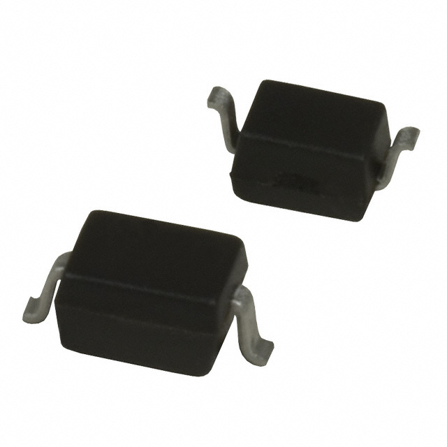
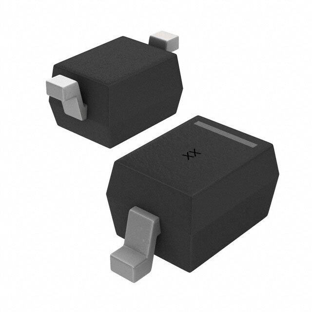
| 描述 | TVS DIODE 5VWM 14.5VC SOD323 |
| 产品分类 | |
| 品牌 | Semtech |
| 数据手册 | |
| 产品图片 |
|
| 产品型号 | SD05.TCT |
| rohs | 无铅 / 符合限制有害物质指令(RoHS)规范要求 |
| 产品系列 | - |
| 不同频率时的电容 | 350pF @ 1MHz |
| 产品目录页面 | |
| 供应商器件封装 | SOD-323 |
| 其它名称 | SD05CT |
| 功率-峰值脉冲 | 350W |
| 包装 | 剪切带 (CT) |
| 单向通道 | 1 |
| 双向通道 | - |
| 安装类型 | 表面贴装 |
| 封装/外壳 | SC-76,SOD-323 |
| 工作温度 | -55°C ~ 125°C (TJ) |
| 应用 | 通用 |
| 标准包装 | 1 |
| 电压-击穿(最小值) | 6V |
| 电压-反向关态(典型值) | 5V(最小值) |
| 电压-箝位(最大值)@Ipp | 14.5V |
| 电流-峰值脉冲(10/1000µs) | 24A (8/20µs) |
| 电源线路保护 | 无 |
| 类型 | 齐纳 |


- 商务部:美国ITC正式对集成电路等产品启动337调查
- 曝三星4nm工艺存在良率问题 高通将骁龙8 Gen1或转产台积电
- 太阳诱电将投资9.5亿元在常州建新厂生产MLCC 预计2023年完工
- 英特尔发布欧洲新工厂建设计划 深化IDM 2.0 战略
- 台积电先进制程称霸业界 有大客户加持明年业绩稳了
- 达到5530亿美元!SIA预计今年全球半导体销售额将创下新高
- 英特尔拟将自动驾驶子公司Mobileye上市 估值或超500亿美元
- 三星加码芯片和SET,合并消费电子和移动部门,撤换高东真等 CEO
- 三星电子宣布重大人事变动 还合并消费电子和移动部门
- 海关总署:前11个月进口集成电路产品价值2.52万亿元 增长14.8%


PDF Datasheet 数据手册内容提取
SD05 and SD12 Single Line TVS Diode for ESD Protection in Portable Electronics PPRROOTTEECCTTIIOONN PPRROODDUUCCTTSS Description Features The SDxx TVS diodes are designed to replace multilayer (cid:139) 350 Watts peak pulse power (t = 8/20µs) p varistors (MLVs) in portable applications such as cell (cid:139) Transient protection for data lines to phones, notebook computers, and PDA’s. They offer IEC 61000-4-2 (ESD) ±25kV (air), ±10kV (contact) superior electrical characteristics such as lower clamp- IEC 61000-4-4 (EFT) 40A (5/50ns) ing voltage and no device degradation when compared IEC 61000-4-5 (Lightning) 24A (8/20µs) to MLVs. The SDxx series TVS diodes are designed to (cid:139) Small package for use in portable electronics protect sensitive semiconductor components from (cid:139) Suitable replacement for MLV’s in ESD protection damage or upset due to electrostatic discharge (ESD) applications and other voltage induced transient events. (cid:139) Protects one I/O or power line (cid:139) Low clamping voltage The SDxx is in a SOD-323 package and will protect one (cid:139) Working voltages: 5V and 12V unidirectional line. They are available with working (cid:139) Low leakage current voltages of 5 volts (SD05) and 12 volts (SD12). These (cid:139) Solid-state silicon-avalanche technology devices will fit on the same PCB pad area as an 0805 MLV device. They give the designer the flexibility to Mechanical Characteristics protect one line in applications where arrays are not (cid:139) EIAJ SOD-323 package practical. Additionally, it may be “sprinkled” around the (cid:139) Molding compound flammability rating: UL 94V-0 board in applications where board space is at a pre- (cid:139) Marking : Marking code, cathode band mium. (cid:139) Packaging : Tape and Reel per EIA 481 They may be used to meet the ESD immunity require- Applications ments of IEC 61000-4-2, Level 4 (±15kV air, ±8kV (cid:139) Cell Phone Handsets and Accessories contact discharge). (cid:139) Microprocessor based equipment (cid:139) Personal Digital Assistants (PDA’s) (cid:139) Notebooks, Desktops, and Servers (cid:139) Portable Instrumentation (cid:139) Pagers Peripherals Schematic & PIN Configuration SOD-323 (Top View) Revision 07/12/04 1 www.semtech.com
SD05 and SD12 PPRROOTTEECCTTIIOONN PPRROODDUUCCTTSS Absolute Maximum Rating Rating Symbol Value Units PeakPulsePower(t =8/20µs) P 350 Watts p pk ESDVoltage(HBM WaveformperIEC61000-4-2) V 30 kV ESD Lead Soldering Temperature T 260(10sec.) °C L Operating Temperature T -55to+125 °C J StorageTemperature T -55to+150 °C STG Electrical Characteristics SD05 Parameter Symbol Conditions Minimum Typical Maximum Units ReverseStand-Off Voltage V 5 V RWM ReverseBreakdown Voltage V I =1mA 6 V BR t ReverseLeakageCurrent I V =5V, T=25°C 10 µA R RWM Clamping Voltage V I =5A, t =8/20µs 9.8 V C PP p Clamping Voltage V I =24A, t =8/20µs 14.5 V C PP p Peak PulseCurrent I t =8/20µs 24 A PP p Junction Capacitance C V =0V, f =1MHz 350 pF j R SD12 Parameter Symbol Conditions Minimum Typical Maximum Units ReverseStand-Off Voltage V 12 V RWM ReverseBreakdown Voltage V I =1mA 13.3 V BR t ReverseLeakageCurrent I V =12V, T=25°C 1 µA R RWM Clamping Voltage V I =5A, t =8/20µs 19 V C PP p Clamping Voltage V I =15A, t =8/20µs 25 V C PP p Peak PulseCurrent I t =8/20µs 15 A PP p Junction Capacitance C V =0V, f =1MHz 150 pF j R 2004 Semtech Corp. 2 www.semtech.com
SD05 and SD12 PPRROOTTEECCTTIIOONN PPRROODDUUCCTTSS Typical Characteristics Non-Repetitive Peak Pulse Power vs. Pulse Time Power Derating Curve 10 110 100 W) 90 wer - P (kpk 1 Power or IPP 678000 Po ed 50 e at s R 40 k Pul 0.1 % of 30 ea 20 P 10 0 0.01 0 25 50 75 100 125 150 0.1 1 10 100 1000 Ambient Temperature - TA (oC) Pulse Duration - t (µs) p Pulse Waveform Clamping Voltage vs. Peak Pulse Current 110 100 Waveform 30 Parameters Waveform 90 tr = 8µs 25 Parameters nt of IPP 678000 e-t td = 20µs oltage - V (V)C 1250 SD12 tdtr == 280µµss e 50 V Perc 40 td = IPP/2 mping 10 SD05 30 a Cl 20 5 10 0 0 0 5 10 15 20 25 30 0 5 10 15 20 25 30 Peak Pulse Current - IPP (A) Time (µs) Capacitance vs. Reverse Voltage Forward Voltage vs. Forward Current 7.00 350 f = 1MHz 6.00 300 ce - C (pF)j220500 SD05 oltage -V (V)F45..0000 SD12 SD05 an150 d V 3.00 cit war apa100 For 2.00 Waveform C SD12 Parameters: 50 1.00 tr = 8µs td = 10µs 0 0.00 0 2 4 6 8 10 12 14 0 5 10 15 20 25 30 35 40 45 Reverse Voltage - VR (V) Forward Current - IF (A) 2004 Semtech Corp. 3 www.semtech.com
SD05 and SD12 PPRROOTTEECCTTIIOONN PPRROODDUUCCTTSS Applications Information Device Connection Options Device Schematic and Pin Configuration The SDxx TVS diodes are designed to protect one data, I/O, or power supply line. The device is designed to replace multi-layer varistors (MLVs) in portable applications. It is easily implemented on existing 0805 MLV pads and is only slightly larger than 0603 MLV pads. The device is unidirectional and may be used on lines where the signal polarity is above ground. The cathode band should be placed towards the line that is to be protected. Size Comparison to 0805 MLV Circuit Board Layout Recommendations for Suppres- sion of ESD. Good circuit board layout is critical for the suppression of fast rise-time transients such as ESD. The following guidelines are recommended (Refer to application note SI99-01 for more detailed information): (cid:122) Place the TVS near the input terminals or connectors to restrict transient coupling. (cid:122) Minimize the path length between the TVS and the protected line. SOD-323 0805 MLV (cid:122) The ESD transient return path to ground should Note: Nominal dimensions in inches be kept as short as possible. (cid:122) Place a TVS and decoupling capacitor between power and ground of components that may be Component Placement Comparison vulnerable to electrostatic discharges to the ground plane. (cid:122) Minimize all conductive loops including power and ground loops. (cid:122) Use multilayer boards when possible. (cid:122) Minimize interconnecting line lengths (cid:122) Never run critical signals near board edges. (cid:122) Fill unused portions of the PCB with ground plane. 0805 MLV on SOD-323 on 0805 SOD-323 on Recommended Matte Tin Lead Finish 0805 Solder Pad MLV Pad (SOD-323) Solder Pad Matte tin has become the industry standard lead-free replacement for SnPb lead finishes. A matte tin finish is composed of 100% tin solder with large grains. Since the solder volume on the leads is small com- pared to the solder paste volume that is placed on the land pattern of the PCB, the reflow profile will be determined by the requirements of the solder paste. Therefore, these devices are compatible with both lead-free and SnPb assembly techniques. In addition, unlike other lead-free compositions, matte tin does not have any added alloys that can cause degradation of the solder joint. 2004 Semtech Corp. 4 www.semtech.com
SD05 and SD12 PPRROOTTEECCTTIIOONN PPRROODDUUCCTTSS Outline Drawing Land Pattern 2004 Semtech Corp. 5 www.semtech.com
SD05 and SD12 PPRROOTTEECCTTIIOONN PPRROODDUUCCTTSS Marking Codes Marking Part Number Code SD05 5U SD12 6U Ordering Information Part Qtyper Lead Finish ReelSize Number Reel SD05.TC SnPb 3,000 7” SD12.TC SnPb 3,000 7” SD05.TCT Pb free 3,000 7” SD12.TCT Pb free 3,000 7” Contact Information Semtech Corporation Protection Products Division 200 Flynn Rd., Camarillo, CA 93012 Phone: (805)498-2111 FAX (805)498-3804 2004 Semtech Corp. 6 www.semtech.com