ICGOO在线商城 > 集成电路(IC) > 数据采集 - ADCs/DAC - 专用型 > PCM1804DB
 Datasheet下载
- 型号: PCM1804DB
- 制造商: Texas Instruments
- 库位|库存: xxxx|xxxx
- 要求:
| 数量阶梯 | 香港交货 | 国内含税 |
| +xxxx | $xxxx | ¥xxxx |
查看当月历史价格
查看今年历史价格
PCM1804DB产品简介:
ICGOO电子元器件商城为您提供PCM1804DB由Texas Instruments设计生产,在icgoo商城现货销售,并且可以通过原厂、代理商等渠道进行代购。 PCM1804DB价格参考¥22.66-¥42.10。Texas InstrumentsPCM1804DB封装/规格:数据采集 - ADCs/DAC - 专用型, ADC,音频 24 b 192k I²S 28-SSOP。您可以下载PCM1804DB参考资料、Datasheet数据手册功能说明书,资料中有PCM1804DB 详细功能的应用电路图电压和使用方法及教程。
PCM1804DB是德州仪器(Texas Instruments)生产的一款专用型数据采集ADC(模数转换器),主要用于音频信号处理领域。该器件具备高精度、低噪声和低失真的特点,适用于需要高质量音频输入的设备。

 主要应用场景:

1. 专业音频设备:
   - PCM1804DB广泛应用于专业音频设备中,如录音机、调音台、音频接口等。它能够提供高达24位分辨率和高达192kHz的采样率,确保音频信号在数字化过程中保持高保真度。

2. 消费级音频产品:
   - 在消费级音频产品中,PCM1804DB可用于高端耳机放大器、便携式音乐播放器、家庭影院系统等。其低功耗设计使得它在便携式设备中也有很好的应用前景,能够在保证音频质量的同时延长电池寿命。

3. 语音识别与通信设备:
   - 由于其高信噪比和低失真特性,PCM1804DB也适用于语音识别和通信设备。例如,在智能音箱、电话会议系统和车载通信系统中,它可以确保语音信号的清晰传输,提升用户体验。

4. 医疗设备中的音频采集:
   - 在医疗设备中,如听诊器或超声波设备,PCM1804DB可以用于高质量的音频信号采集。它的高精度和低噪声特性有助于提高诊断的准确性。

5. 工业自动化与监控系统:
   - 在工业环境中,PCM1804DB可以用于声音监测和分析系统,如噪音水平监测、机械故障预测等。它能够精确地捕捉环境中的声音变化,帮助工程师进行数据分析和故障诊断。

 总结:
PCM1804DB凭借其高性能和低功耗的特点,适用于多种需要高质量音频信号采集的应用场景,包括专业音频设备、消费级音频产品、语音识别与通信设备、医疗设备以及工业自动化与监控系统。
| 参数 | 数值 |
| ADC输入端数量 | 2 |
| 产品目录 | 集成电路 (IC)半导体 |
| 描述 | IC ADC DLTASGMA AUD 24BIT 28SSOP音频模/数转换器 IC Full Diff Anlg Inp 24-Bit 192KHz Ster |
| DevelopmentKit | DEM-DAI1804 |
| 产品分类 | |
| 品牌 | Texas Instruments |
| 产品手册 | http://www.ti.com/litv/sles022c |
| 产品图片 |
|
| rohs | 符合RoHS无铅 / 符合限制有害物质指令(RoHS)规范要求 |
| 产品系列 | 音频 IC,音频模/数转换器 IC,Texas Instruments PCM1804DB- |
| 数据手册 | |
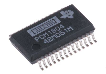
| 产品型号 | PCM1804DB |
| 产品培训模块 | http://www.digikey.cn/PTM/IndividualPTM.page?site=cn&lang=zhs&ptm=13240 |
| 产品目录页面 | |
| 产品种类 | 音频模/数转换器 IC |
| 供应商器件封装 | 28-SSOP |
| 信噪比 | 111 dB |
| 其它名称 | 296-12455-5 |
| 分辨率 | 24 bit |
| 分辨率(位) | 24 b |
| 制造商产品页 | http://www.ti.com/general/docs/suppproductinfo.tsp?distId=10&orderablePartNumber=PCM1804DB |
| 功耗 | 265 mW |
| 包装 | 管件 |
| 单位重量 | 285.800 mg |
| 商标 | Texas Instruments |
| 安装类型 | 表面贴装 |
| 安装风格 | SMD/SMT |
| 封装 | Tube |
| 封装/外壳 | 28-SSOP(0.209",5.30mm 宽) |
| 封装/箱体 | SSOP-28 |
| 工作温度 | -10°C ~ 70°C |
| 工作电源电压 | 5 V |
| 工厂包装数量 | 47 |
| 数据接口 | 串行 |
| 最大功率耗散 | 290 mW |
| 最大工作温度 | + 70 C |
| 最小工作温度 | - 10 C |
| 标准包装 | 47 |
| 电压-电源 | 3 V ~ 3.6 V,4.75 V ~ 5.25 V |
| 电压源 | 模拟和数字 |
| 电源电压-最大 | 5.25 V |
| 电源电压-最小 | 4.75 V |
| 类型 | ADC, 音频 |
| 系列 | PCM1804 |
| 转换器数量 | 2 |
| 转换速率 | 192 kHz |
| 配用 | /product-detail/zh/DEM-DAI1804/DEM-DAI1804-ND/1898340 |
| 采样率(每秒) | 192k |


- 商务部:美国ITC正式对集成电路等产品启动337调查
- 曝三星4nm工艺存在良率问题 高通将骁龙8 Gen1或转产台积电
- 太阳诱电将投资9.5亿元在常州建新厂生产MLCC 预计2023年完工
- 英特尔发布欧洲新工厂建设计划 深化IDM 2.0 战略
- 台积电先进制程称霸业界 有大客户加持明年业绩稳了
- 达到5530亿美元!SIA预计今年全球半导体销售额将创下新高
- 英特尔拟将自动驾驶子公司Mobileye上市 估值或超500亿美元
- 三星加码芯片和SET,合并消费电子和移动部门,撤换高东真等 CEO
- 三星电子宣布重大人事变动 还合并消费电子和移动部门
- 海关总署:前11个月进口集成电路产品价值2.52万亿元 增长14.8%


PDF Datasheet 数据手册内容提取
(cid:2)(cid:17)(cid:14)(cid:14)(cid:20)(cid:2)(cid:14)(cid:13)(cid:18)(cid:12) (cid:4)(cid:14)(cid:13)(cid:8)(cid:17)(cid:7)(cid:16)(cid:15) (cid:10)(cid:14)(cid:13)(cid:11) (cid:5)(cid:9)(cid:19)(cid:6)(cid:15) (cid:3)(cid:12)(cid:15)(cid:16)(cid:14)(cid:17)(cid:11)(cid:9)(cid:12)(cid:16)(cid:15) PCM1804 SLES022C–DECEMBER2001–REVISEDOCTOBER2007 FULL DIFFERENTIAL ANALOG INPUT 24-BIT, 192-kHz STEREO A/D CONVERTER FEATURES APPLICATIONS 1 • 24-BitDelta-SigmaStereoA/DConverter • AVAmplifier 23 • HighPerformance: • MDPlayer – DynamicRange:112dB(Typical) • DigitalVTR • DigitalMixer – SNR:111dB(Typical) • DigitalRecorder – THD+N:–102dB(Typical) • High-PerformanceLinearPhaseAntialias DESCRIPTION DigitalFilter: The PCM1804 is a high-performance, single-chip – Pass-BandRipple:±0.005dB stereo A/D converter with fully differential analog – Stop-BandAttenuation:–100dB voltage input. The PCM1804 uses a precision • FullyDifferentialAnalogInput:±2.5V delta-sigma modulator and includes a linear phase • AudioInterface:Master-orSlave-Mode antialias digital filter and high-pass filter (HPF) that removes dc offset from the input signal. The Selectable PCM1804 is suitable for a wide variety of mid- to • DataFormats:Left-Justified,I2S,Standard high-grade consumer and professional applications, 24-Bit,andDSD where excellent performance and 5-V analog supply • Function: and3.3-Vdigitalpower-supplyoperation are required. The PCM1804 can achieve both PCM audio and – PeakDetection DSD format due to the precision delta-sigma – High-PassFilter(HPF):–3dBat1Hz, modulator. The PCM1804 is fabricated using an fS=48kHz advanced CMOS process and is available in a small • SamplingRateupto192kHz 28-pinSSOPpackage. • SystemClock:128f ,256f ,384f , S S S 512f ,or768f S S • DualPowerSupplies: – 5VforAnalog – 3.3VforDigital • PowerDissipation:225mW • Small28-PinSSOP • DSDOutput:1Bit,64f S 1 Pleasebeawarethatanimportantnoticeconcerningavailability,standardwarranty,anduseincriticalapplicationsof TexasInstrumentssemiconductorproductsanddisclaimerstheretoappearsattheendofthisdatasheet. SystemTwo,AudioPrecisionaretrademarksofAudioPrecision,Inc. 2 Allothertrademarksarethepropertyoftheirrespectiveowners. 3 PRODUCTIONDATAinformationiscurrentasofpublicationdate. Copyright©2001–2007,TexasInstrumentsIncorporated Products conform to specifications per the terms of the Texas Instruments standard warranty. Production processing does not necessarilyincludetestingofallparameters.
PCM1804 www.ti.com SLES022C–DECEMBER2001–REVISEDOCTOBER2007 This device contains circuits to protect its inputs and outputs against damage due to high static voltages or electrostatic fields. These circuits have been qualified to protect this device against electrostatic discharges (ESD) of up to 2 kV according to MIL-STD-883C, Method 3015; however, it is advised that precautions be taken to avoid application of any voltage higher than maximum-ratedvoltagestothesehigh-impedancecircuits.Duringstorageorhandling,thedeviceleadsshouldbeshortedtogether orthedeviceshouldbeplacedinconductivefoam.Inacircuit,unusedinputsshouldalwaysbeconnectedtoanappropriatelogic voltagelevel,preferablyeitherV orground.Specificguidelinesforhandlingdevicesofthistypearecontainedinthepublication CC ElectrostaticDischarge(ESD)(SSYA008),availablefromTexasInstruments. PIN ASSIGNMENTS PCM1804 PACKAGE (TOP VIEW) V L 1 28 V R REF REF AGNDL 2 27 AGNDR V L 3 26 V R COM COM V L+ 4 25 V R+ IN IN V L− 5 24 V R− IN IN FMT0 6 23 AGND FMT1 7 22 V CC S/M 8 21 OVFL OSR0 9 20 OVFR OSR1 10 19 RST OSR2 11 18 SCKI BYPAS 12 17 LRCK/DSDBCK DGND 13 16 BCK/DSDL VDD 14 15 DATA/DSDR P0007-02 2 SubmitDocumentationFeedback Copyright©2001–2007,TexasInstrumentsIncorporated ProductFolderLink(s):PCM1804
PCM1804 www.ti.com SLES022C–DECEMBER2001–REVISEDOCTOBER2007 FUNCTIONALBLOCKDIAGRAM OSR0 CLK SCKI OSR1 Control OSR2 VINL+ Delta-Sigma Decimation Modulator (L) HPF S/M VINL− Filter (L) FMT0 VCOML FMT1 AGNDL VREFL VREFL Serial LRCK/DSDBCK Output Interface BCK/DSDL VREFR VREFR AGNDR DATA/DSDR VCOMR VINR+ Delta-Sigma Decimation HPF OVFL Filter (R) Modulator (R) VINR− OVFR BYPAS Power Supply RST VCC AGND DGND VDD B0029-01 Copyright©2001–2007,TexasInstrumentsIncorporated SubmitDocumentationFeedback 3 ProductFolderLink(s):PCM1804
PCM1804 www.ti.com SLES022C–DECEMBER2001–REVISEDOCTOBER2007 TerminalFunctions TERMINAL I/O DESCRIPTIONS NAME PIN AGND 23 – Analogground AGNDL 2 – AnaloggroundforV L REF AGNDR 27 – AnaloggroundforV R REF BCK/DSDL 16 I/O Bitclockinput/outputinPCMmode.L-channelaudiodataoutputinDSDmode. (1) BYPAS 12 I HPFbypasscontrol.High:HPFdisabled,Low:HPFenabled (1) DATA/DSDR 15 O L-channelandR-channelaudiodataoutputinPCMmode.R-channelaudiodataoutputinDSDmode.(DSD output,wheninDSDmode) DGND 13 – Digitalground FMT0 6 I Audiodataformat0.SeeTable5. (2) FMT1 7 I Audiodataformat1.SeeTable5. (2) LRCK/DSDBCK 17 I/O Samplingclockinput/outputinPCMandDSDmodes. (1) OSR0 9 I Oversamplingratio0.SeeTable1andTable2. (2) OSR1 10 I Oversamplingratio1.SeeTable1andTable2. (2) OSR2 11 I Oversamplingratio2.SeeTable1andTable2. (2) OVFL 21 O OverflowsignalofL-channelinPCMmode.ThisisavailableinPCMmodeonly. OVFR 20 O OverflowsignalofR-channelinPCMmode.ThisisavailableinPCMmodeonly. RST 19 I Reset,power-downinput,active-low (2) SCKI 18 I Systemclockinput;128f ,256f ,384f ,512f ,or768f . (3) S S S S S S/M 8 I Slave/mastermodeselection.SeeTable4. (2) V 22 – Analogpowersupply CC V L 3 – L-channelanalogcommon-modevoltage(2.5V) COM V R 26 – R-channelanalogcommon-modevoltage(2.5V) COM V 14 – Digitalpowersupply DD V L– 5 I L-channelanaloginput,negativepin IN V L+ 4 I L-channelanaloginput,positivepin IN V R– 24 I R-channelanaloginput,negativepin IN V R+ 25 I R-channelanaloginput,positivepin IN V L 1 – L-channelvoltagereferenceoutput,requirescapacitorsfordecouplingtoAGND REF V R 28 – R-channelvoltagereferenceoutput,requirescapacitorsfordecouplingtoAGND REF (1) Schmitt-triggerinput (2) Schmitt-triggerinputwithinternalpulldown(51kμtypically),5-Vtolerant. (3) Schmitt-triggerinput,5-Vtolerant. 4 SubmitDocumentationFeedback Copyright©2001–2007,TexasInstrumentsIncorporated ProductFolderLink(s):PCM1804
PCM1804 www.ti.com SLES022C–DECEMBER2001–REVISEDOCTOBER2007 ABSOLUTE MAXIMUM RATINGS overoperatingfree-airtemperaturerange(unlessotherwisenoted)(1) V –0.3Vto6.5V CC Supplyvoltage V –0.3Vto4V DD Groundvoltagedifferences AGND,AGNDL,AGNDR,DGND ±0.1V Supplyvoltagedifference V ,V V –V <3V CC DD CC DD FMT0,FMT1,S/M,OSR0,OSR1,OSR2,SCKI,RST –0.3Vto6.5V Digitalinputvoltage BYPAS,DATA/DSDR,BCK/DSDL,LRCK/DSDBCK,OVFL,OVFR –0.3Vto(V +0.3V) DD Analoginputvoltage V L,V R,V L,V R,V L+,V R+,V L–,V R– –0.3Vto(V +0.3V) REF REF COM COM IN IN IN IN CC Inputcurrent(anypinsexceptsupplies) ±10mA T Ambienttemperatureunderbias –40(cid:176) Cto125(cid:176) C A T Storagetemperature –55(cid:176) Cto150(cid:176) C stg T Junctiontemperature 150(cid:176) C J Leadtemperature(soldering) 260(cid:176) C,5s Packagetemperature(IRreflow,peak) 260(cid:176) C (1) Stressesbeyondthoselistedunder"absolutemaximumratings”maycausepermanentdamagetothedevice.Thesearestressratings only,andfunctionaloperationofthedeviceattheseoranyotherconditionsbeyondthoseindicatedunder"recommendedoperating conditions”isnotimplied.Exposuretoabsolute-maximum-ratedconditionsforextendedperiodsmayaffectdevicereliability. RECOMMENDED OPERATING CONDITIONS overoperatingfree-airtemperaturerange MIN NOM MAX UNIT Analogsupplyvoltage,V 4.75 5 5.25 V CC Digitalsupplyvoltage,V 3 3.3 3.6 V DD Analoginputvoltage,full-scale(–0dB),differentialinput 5 Vp-p Digitalinputlogicfamily TTLcompatible Systemclock 8.192 36.864 MHz Digitalinputclockfrequency Samplingclock 32 192 kHz Digitaloutputloadcapacitance 10 pF Operatingfree-airtemperature,T –10 70 (cid:176) C A Copyright©2001–2007,TexasInstrumentsIncorporated SubmitDocumentationFeedback 5 ProductFolderLink(s):PCM1804
PCM1804 www.ti.com SLES022C–DECEMBER2001–REVISEDOCTOBER2007 ELECTRICAL CHARACTERISTICS AllspecificationsatT =25(cid:176) C,V =5V,V =3.3V,mastermode,single-speedmode,f =48kHz,systemclock=256f , A CC DD S S 24-bitdata,unlessotherwisenoted. PCM1804DB PARAMETER TESTCONDITIONS UNIT MIN TYP MAX Resolution 24 Bits DATAFORMAT Audiodatainterfaceformat Standard,I2S,left-justified Audiodatabitlength 24 Bits MSBfirst, Audiodataformat 2scomplement,DSD DIGITALINPUT/OUTPUT Logicfamily TTLcompatible (1) (2) 2 5.5 V High-levelinputvoltage Vdc IH (3) 2 V DD V Low-levelinputvoltage (1) (2) (3) 0.8 Vdc IL V =V (1) 65 100 IN DD I High-levelinputcurrent V =V (2) ±10 μA IH IN DD V =V (3) ±100 IN DD V =0V (1) (2) ±10 IN I Low-levelinputcurrent μA IL V =0V (3) ±50 IN V High-leveloutputvoltage I =–1mA (4) 2.4 Vdc OH OH V Low-leveloutputvoltage I =1mA (4) 0.4 Vdc OL OL CLOCKFREQUENCY f Samplingfrequency 32 192 kHz S 256f ,singlerate (5) 12.288 S 384f ,singlerate (5) 18.432 S 512f ,singlerate (5) 24.576 S 768f ,singlerate (5) 36.864 S Systemclockfrequency MHz 256f ,dualrate (6) 24.576 S 384f ,dualrate (6) 36.864 S 128f ,quadrate (7) 24.576 S 192f ,quadrate (7) 36.864 S DCACCURACY Gainmismatch,channel- ±3 %ofFSR to-channel Gainerror(V =–0.5dB) ±4 %ofFSR IN Bipolarzeroerror HPFbypass ±0.2 %ofFSR (1) Pins6–11,19:FMT0,FMT1,S/M,OSR0,OSR1,OSR2,RST[Schmitt-triggerinputwithinternalpulldown(51kμtypically),5-Vtolerant] (2) Pin18:SCKI(Schmitt-triggerinput,5-Vtolerant) (3) Pins12,16–17:BYPAS,BCK/DSDL,LRCK/DSDBCK(inslavemode,Schmitt-triggerinput) (4) Pins15–17,20,and21:DATA/DSDR,BCK/DSDL,LRCK/DSDBCK(inmastermode),OVFR,OVFL (5) Singlerate,f =48kHz S (6) Dualrate,f =96kHz S (7) Quadrate,f =192kHz S 6 SubmitDocumentationFeedback Copyright©2001–2007,TexasInstrumentsIncorporated ProductFolderLink(s):PCM1804
PCM1804 www.ti.com SLES022C–DECEMBER2001–REVISEDOCTOBER2007 ELECTRICAL CHARACTERISTICS (continued) AllspecificationsatT =25(cid:176) C,V =5V,V =3.3V,mastermode,single-speedmode,f =48kHz,systemclock=256f , A CC DD S S 24-bitdata,unlessotherwisenoted. PCM1804DB PARAMETER TESTCONDITIONS UNIT MIN TYP MAX DYNAMICPERFORMANCE (8) V =–0.5dB –102 –95 IN f =48kHz,systemclock=256f S S V =–60dB –49 IN V =–0.5dB –101 IN Totalharmonicdistortion fS=96kHz,systemclock=256fS THD+N V =–60dB –47 dB plusnoise IN V =–0.5dB –101 IN f =192kHz,systemclock=128f S S V =–60dB –47 IN V =–0.5dB DSDmode –100 IN f =48kHz,systemclock=256f 106 112 S S Dynamicrange VIN=–60dB fS=96kHz,systemclock=256fS 112 dB (A-weighted) f =192kHz,systemclock=128f 112 S S DSDmode 112 f =48kHz,systemclock=256f 105 111 S S f =96kHz,systemclock=256f 111 S S SNR(A-weighted) dB f =192kHz,systemclock=128f 111 S S DSDmode 111 f =48kHz,systemclock=256f 97 109 S S Channelseparation f =96kHz,systemclock=256f 107 dB S S f =192kHz,systemclock=128f 107 S S ANALOGINPUT Inputvoltage Differentialinput ±2.5 V Centervoltage 2.5 Vdc Inputimpedance Single-ended 10 kμ DIGITALFILTERPERFORMANCE Pass-bandedge Singlerate,dualrate 0.453f Hz S Stop-bandedge Singlerate,dualrate 0.547f Hz S Pass-bandripple Singlerate,dualrate ±0.005 dB Stop-bandattenuation Singlerate,dualrate –100 dB Pass-bandedge(–0.005 Quadrate 0.375f Hz dB) S Pass-bandedge(–3dB) Quadrate 0.49f Hz S Stop-bandedge Quadrate 0.77f Hz S Pass-bandripple Quadrate ±0.005 dB Stop-bandattenuation Quadrate –135 dB Groupdelay Singlerate,dualrate 37/f s S Groupdelay Quadrate 9.5/f s S HPFfrequencyresponse –3dB f /48000 Hz S (8) f =1kHz,usingSystemTwo™audiomeasurementsystembyAudioPrecision™inRMSmode,with20-kHzLPFand400-HzHPFin IN calculationforsinglerate,orwith40-kHzLPFincalculationfordualandquadrates. Copyright©2001–2007,TexasInstrumentsIncorporated SubmitDocumentationFeedback 7 ProductFolderLink(s):PCM1804
PCM1804 www.ti.com SLES022C–DECEMBER2001–REVISEDOCTOBER2007 ELECTRICAL CHARACTERISTICS (continued) AllspecificationsatT =25(cid:176) C,V =5V,V =3.3V,mastermode,single-speedmode,f =48kHz,systemclock=256f , A CC DD S S 24-bitdata,unlessotherwisenoted. PCM1804DB PARAMETER TESTCONDITIONS UNIT MIN TYP MAX POWERSUPPLYREQUIREMENTS V 4.75 5 5.25 CC Supplyvoltagerange Vdc V 3 3.3 3.6 DD I V =5V (9) (10) (11) 35 45 CC CC V =3.3V (9) (12) 15 20 DD Supplycurrent mA I V =3.3V (10) (12) 27 DD DD V =3.3V (11) (12) 18 DD Operation,V =5V,V =3.3V (9) (12) 225 290 CC DD Operation,V =5V,V =3.3V (10) (12) 265 CC DD P Powerdissipation mW D Operation,V =5V,V =3.3V (11) (12) 235 CC DD Powerdown,V =5V,V =3.3V 5 CC DD TEMPERATURERANGE Operationtemperature –10 70 (cid:176) C θ Thermalresistance 100 (cid:176) C/W JA (9) Singlerate,f =48kHz S (10) Dualrate,f =96kHz S (11) Quadrate,f =192kHz S (12) MinimumloadonDATA/DSDR(pin15) 8 SubmitDocumentationFeedback Copyright©2001–2007,TexasInstrumentsIncorporated ProductFolderLink(s):PCM1804
PCM1804 www.ti.com SLES022C–DECEMBER2001–REVISEDOCTOBER2007 TYPICAL PERFORMANCE CURVES - SINGLE RATE AllspecificationsatT =25(cid:176) C,V =3.3V,V =5V,mastermode,f =48kHz,systemclock=256f ,24-bitdata,unless A CC DD S S otherwisenoted. TOTALHARMONICDISTORTION+NOISE DYNAMICRANGEANDSNR vs vs TEMPERATURE TEMPERATURE B) B) 120 0.5 d −90 −35 60 d − − B ( B ( d d − − B on + Noise −95 −40 on + Noise d SNR − d 115 Dynamic Range Distorti −100 −0.5 dB −45 Distorti nge an 110 SNR c c a otal Harmoni −105 −60 dB −50 otal Harmoni Dynamic R 105 T T − − N N D+ −110 −55 D+ TH −20 0 20 40 60 80 TH 100 T − Temperature − °C −20 0 20 40 60 80 G001 T − Temperature − °C G002 Figure1. Figure2. TOTALHARMONICDISTORTION+NOISE DYNAMICRANGEANDSNR vs vs SUPPLYVOLTAGE SUPPLYVOLTAGE B) B) 120 0.5 d −90 −35 60 d − − B ( B ( d d − − B on + Noise −95 −40 on + Noise d SNR − d 115 Dynamic Range Distorti −100 −0.5 dB −45 Distorti nge an 110 SNR c c a otal Harmoni −105 −60 dB −50 otal Harmoni Dynamic R 105 T T − − N N D+ −110 −55 D+ TH 4.50 4.75 5.00 5.25 5.50 TH 100 VCC − Supply Voltage − V 4.50 4.75 5.00 5.25 5.50 G003 VCC − Supply Voltage − V G004 Figure3. Figure4. Copyright©2001–2007,TexasInstrumentsIncorporated SubmitDocumentationFeedback 9 ProductFolderLink(s):PCM1804
PCM1804 www.ti.com SLES022C–DECEMBER2001–REVISEDOCTOBER2007 TYPICAL PERFORMANCE CURVES - SINGLE RATE (continued) AllspecificationsatT =25(cid:176) C,V =3.3V,V =5V,mastermode,f =48kHz,systemclock=256f ,24-bitdata,unless A CC DD S S otherwisenoted. TOTALHARMONICDISTORTION+NOISE DYNAMICRANGEANDSNR vs vs SAMPLINGFREQUENCY SAMPLINGFREQUENCY B) B) 120 0.5 d −90 −35 60 d − − B ( B ( d d − − B on + Noise −95 −40 on + Noise d SNR − d 115 Dynamic Range Distorti −100 −0.5 dB −45 Distorti nge an 110 SNR c c a otal Harmoni −105 −60 dB −50 otal Harmoni Dynamic R 105 T T − − N N D+ −110 −55 D+ TH 32 44.1 48 TH 100 fS − Sampling Frequency − kHz 32 44.1 48 G005 fS − Sampling Frequency − kHz G006 Figure5. Figure6. TOTALHARMONICDISTORTION+NOISE vs SIGNALLEVEL 0 B d − e s −20 oi N + n o −40 rti o st Di c −60 ni o m r Ha −80 al ot T N − −100 + D H T −120 −100 −80 −60 −40 −20 0 Signal Level − dB G009 Figure7. 10 SubmitDocumentationFeedback Copyright©2001–2007,TexasInstrumentsIncorporated ProductFolderLink(s):PCM1804
PCM1804 www.ti.com SLES022C–DECEMBER2001–REVISEDOCTOBER2007 TYPICAL PERFORMANCE CURVES - SINGLE RATE (continued) AllspecificationsatT =25(cid:176) C,V =3.3V,V =5V,mastermode,f =48kHz,systemclock=256f ,24-bitdata,unless A CC DD S S otherwisenoted. AMPLITUDE AMPLITUDE vs vs FREQUENCY FREQUENCY 0 0 Output Spectrum: −20 −20 −0.5 dB, N = 8192 −40 −40 Output Spectrum: B −60 B −60 d d −60 dB, − − e e N = 8192 d −80 d −80 u u plit plit m −100 m −100 A A −120 −120 −140 −140 −160 −160 0 12000 24000 0 12000 24000 f − Frequency − Hz f − Frequency − Hz G007 G008 Figure8. Figure9. TYPICAL PERFORMANCE CURVES - DUAL RATE AllspecificationsatT =25(cid:176) C,V =3.3V,V =5V,mastermode,and24-bitdata,unlessotherwisenoted. A CC DD AMPLITUDE AMPLITUDE vs vs FREQUENCY FREQUENCY 0 0 fS = 96 kHz, fS = 96 kHz, −20 System Clock = 256 fS −20 System Clock = 256 fS −40 −40 Output Spectrum: Output Spectrum: B −60 B −60 d −0.5 dB, d −60 dB, − − e N = 8192 e N = 8192 d −80 d −80 u u plit plit m −100 m −100 A A −120 −120 −140 −140 −160 −160 0 24000 48000 0 24000 48000 f − Frequency − Hz f − Frequency − Hz G010 G011 Figure10. Figure11. Copyright©2001–2007,TexasInstrumentsIncorporated SubmitDocumentationFeedback 11 ProductFolderLink(s):PCM1804
PCM1804 www.ti.com SLES022C–DECEMBER2001–REVISEDOCTOBER2007 TYPICAL PERFORMANCE CURVES - QUAD RATE AllspecificationsatT =25(cid:176) C,V =3.3V,V =5V,mastermode,24-bitdata,unlessotherwisenoted. A CC DD AMPLITUDE AMPLITUDE vs vs FREQUENCY FREQUENCY 0 0 fS = 192 kHz, fS = 192 kHz, −20 System Clock = 128 fS −20 System Clock = 128 fS −40 −40 Output Spectrum: Output Spectrum: B −60 B −60 d −0.5 dB, d −60 dB, − − e N = 8192 e N = 8192 d −80 d −80 u u plit plit m −100 m −100 A A −120 −120 −140 −140 −160 −160 0 48000 96000 0 48000 96000 f − Frequency − Hz f − Frequency − Hz G012 G013 Figure12. Figure13. TYPICAL PERFORMANCE CURVES - DSD MODE AllspecificationsatT =25(cid:176) C,V =3.3V,V =5V,mastermode,f =44.1kHz,systemclock=16.9344MHz,unless A CC DD S otherwisenoted. AMPLITUDE AMPLITUDE vs vs FREQUENCY FREQUENCY 0 0 −20 −20 −40 −40 B −60 B −60 d d e − Output Spectrum: e − Output Spectrum: d −80 −0.5 dB, d −80 −60 dB, u u plit N = 8192 plit N = 8192 m −100 m −100 A A −120 −120 −140 −140 −160 −160 0 11025 22050 0 11025 22050 f − Frequency − Hz f − Frequency − Hz G014 G015 Figure14. Figure15. 12 SubmitDocumentationFeedback Copyright©2001–2007,TexasInstrumentsIncorporated ProductFolderLink(s):PCM1804
PCM1804 www.ti.com SLES022C–DECEMBER2001–REVISEDOCTOBER2007 TYPICAL PERFORMANCE CURVES OF INTERNAL FILTER LINEAR PHASE ANTIALIAS DIGITAL FILTER FREQUENCY RESPONSE - Single-Rate OVERALLCHARACTERISTICS STOP-BANDATTENUATIONCHARACTERISTICS FORSINGLE-RATEFILTER FORSINGLE-RATEFILTER 50 0 fS = 48 kHz −10 fS = 48 kHz −20 0 −30 −40 −50 B B d −50 d −60 − − e e −70 d d mplitu −100 mplitu −−9800 A A −100 −110 −150 −120 −130 −140 −200 −150 0.0 0.5 1.0 1.5 2.0 2.5 3.0 3.5 4.0 0.00 0.25 0.50 0.75 1.00 Normalized Frequency − (cid:1) fS Normalized Frequency − (cid:1) fS G016 G017 Figure16. Figure17. PASS-BANDRIPPLECHARACTERISTICS TRANSIENTBANDCHARACTERISTICS FORSINGLE-RATEFILTER FORSINGLE-RATEFILTER 0.02 0 fS = 48 kHz fS = 48 kHz −1 0.00 −2 −3 −0.02 B B d d −4 − − e e d −0.04 d −5 u u mplit mplit −6 −6.04 dB at 0.5 fS A A −0.06 −7 −8 −0.08 −9 −0.10 −10 0.0 0.1 0.2 0.3 0.4 0.5 0.6 0.45 0.47 0.49 0.51 0.53 0.55 Normalized Frequency − (cid:1) fS Normalized Frequency − (cid:1) fS G018 G019 Figure18. Figure19. Copyright©2001–2007,TexasInstrumentsIncorporated SubmitDocumentationFeedback 13 ProductFolderLink(s):PCM1804
PCM1804 www.ti.com SLES022C–DECEMBER2001–REVISEDOCTOBER2007 TYPICAL PERFORMANCE CURVES OF INTERNAL FILTER (continued) LINEAR PHASE ANTIALIAS DIGITAL FILTER FREQUENCY RESPONSE - Dual-Rate OVERALLCHARACTERISTICS STOP-BANDATTENUATIONCHARACTERISTICS FORDUAL-RATEFILTER FORDUAL-RATEFILTER 50 0 −10 fS = 96 kHz fS = 96 kHz −20 0 −30 −40 −50 B B d −50 d −60 − − e e −70 d d mplitu −100 mplitu −−9800 A A −100 −110 −150 −120 −130 −140 −200 −150 0.0 0.2 0.4 0.6 0.8 1.0 1.2 1.4 1.6 1.8 2.0 0.00 0.25 0.50 0.75 1.00 Normalized Frequency − (cid:1) fS Normalized Frequency − (cid:1) fS G020 G021 Figure20. Figure21. PASS-BANDRIPPLECHARACTERISTICS TRANSIENTBANDCHARACTERISTICS FORDUAL-RATEFILTER FORDUAL-RATEFILTER 0.02 0 fS = 96 kHz fS = 96 kHz −1 0.00 −2 −3 −0.02 B B d d −4 − − e e d −0.04 d −5 u u mplit mplit −6 −6.02 dB at 0.5 fS A A −0.06 −7 −8 −0.08 −9 −0.10 −10 0.0 0.1 0.2 0.3 0.4 0.5 0.6 0.45 0.47 0.49 0.51 0.53 0.55 Normalized Frequency − (cid:1) fS Normalized Frequency − (cid:1) fS G022 G023 Figure22. Figure23. 14 SubmitDocumentationFeedback Copyright©2001–2007,TexasInstrumentsIncorporated ProductFolderLink(s):PCM1804
PCM1804 www.ti.com SLES022C–DECEMBER2001–REVISEDOCTOBER2007 TYPICAL PERFORMANCE CURVES OF INTERNAL FILTER (continued) LINEAR PHASE ANTIALIAS DIGITAL FILTER FREQUENCY RESPONSE - Quad-Rate OVERALLCHARACTERISTICS STOP-BANDATTENUATIONCHARACTERISTICS FORQUAD-RATEFILTER FORQUAD-RATEFILTER 50 0 −10 fS = 192 kHz fS = 192 kHz −20 0 −30 −40 −50 B B d −50 d −60 − − e e −70 d d mplitu −100 mplitu −−9800 A A −100 −110 −150 −120 −130 −140 −200 −150 0.0 0.1 0.2 0.3 0.4 0.5 0.6 0.7 0.8 0.9 1.0 0.00 0.25 0.50 0.75 1.00 Normalized Frequency − (cid:1) fS Normalized Frequency − (cid:1) fS G024 G025 Figure24. Figure25. PASS-BANDRIPPLECHARACTERISTICS TRANSIENTBANDCHARACTERISTICS FORQUAD-RATEFILTER FORQUAD-RATEFILTER 0.02 0 fS = 192 kHz fS = 192 kHz −1 0.00 −2 −3 −0.02 B B d d −4 − − e e d −0.04 d −5 u u mplit mplit −6 −3.9 dB at 0.5 fS A −0.06 A −7 −8 −0.08 −9 −0.10 −10 0.0 0.1 0.2 0.3 0.4 0.5 0.6 0.45 0.47 0.49 0.51 0.53 0.55 Normalized Frequency − (cid:1) fS Normalized Frequency − (cid:1) fS G026 G027 Figure26. Figure27. Copyright©2001–2007,TexasInstrumentsIncorporated SubmitDocumentationFeedback 15 ProductFolderLink(s):PCM1804
PCM1804 www.ti.com SLES022C–DECEMBER2001–REVISEDOCTOBER2007 TYPICAL PERFORMANCE CURVES OF INTERNAL FILTER (continued) HIGH-PASS FILTER (HPF) FREQUENCY RESPONSE STOP-BANDCHARACTERISTICS PASS-BANDCHARACTERISTICS 0 0.2 −10 0.0 −20 −30 −0.2 B B d −40 d − − e e d −50 d −0.4 u u mplit −60 mplit A A −0.6 −70 −80 −0.8 −90 −100 −1.0 0.0 0.1 0.2 0.3 0.4 0.0 0.5 1.0 1.5 2.0 2.5 3.0 3.5 4.0 Normalized Frequency − (cid:1) fS/1000 Normalized Frequency − (cid:1) fS/1000 G028 G029 Figure28. Figure29. PRINCIPLES OF OPERATION THEORY OF OPERATION The PCM1804 consists of a band-gap reference, a delta-sigma modulator with full-differential architecture for L-channel and R-channel, a decimation filter with a high-pass filter, and a serial interface circuit. Figure 30 illustrates the total architecture of the PCM1804. An on-chip, high-precision reference with 10-μF external capacitor(s)providesallthereferencevoltageneededinthePCM1804,anditdefinesthefull-scale voltage range of both channels. Full-differential architecture provides a wide dynamic range and excellent power-supply rejection performance. The input signal is sampled at · 128, · 64, and · 32 oversampling rates according to the overasmplingratiocontrol,OSR[0:2].Thesingle rate, dual rate, and quad rate eliminate the external sample-hold amplifier. Figure 31 illustrates how for each oversampling ratio the PCM1804 decimates the modulator output down to PCM data when the modulator is running at 6.144 MHz. The delta-sigma modulation randomizes the modulator outputs and reduces the idle tone level. The oversampled data stream from the delta-sigma modulator is converted to a 1-f , 24-bit digital signal, while removing high-frequency noise components using a decimation S filter. The dc components of the signal are removed by the HPF, and the HPF output is converted to a time-multiplexed serial signal through the serial interface, which provides flexible serial formats and master/slave modes. The PCM1804 also has a DSD output mode. The PCM1804 can output the signal directly from the modulatorstoDSDL(pin16)andDSDR(pin15). 16 SubmitDocumentationFeedback Copyright©2001–2007,TexasInstrumentsIncorporated ProductFolderLink(s):PCM1804
PCM1804 www.ti.com SLES022C–DECEMBER2001–REVISEDOCTOBER2007 PRINCIPLES OF OPERATION (continued) OSR0 CLK SCKI OSR1 Control OSR2 VINL+ Delta-Sigma Decimation Modulator (L) HPF S/M VINL− Filter (L) FMT0 VCOML FMT1 AGNDL VREFL VREFL Serial LRCK/DSDBCK Output Interface BCK/DSDL VREFR VREFR AGNDR DATA/DSDR VCOMR VINR+ Delta-Sigma Decimation HPF OVFL Filter (R) Modulator (R) VINR− OVFR BYPAS Power Supply RST VCC AGND DGND VDD B0029-01 Figure30.TotalBlockDiagramofPCM1804 0 Quad-Rate Filter −20 −40 B Dual-Rate Filter d −60 − e Modulator d Single- plitu −80 FRilateter m A −100 −120 −140 −160 0 48 96 144 192 f − Frequency − kHz G030 Figure31.SpectrumofModulatorOutputandDecimationFilter Copyright©2001–2007,TexasInstrumentsIncorporated SubmitDocumentationFeedback 17 ProductFolderLink(s):PCM1804
PCM1804 www.ti.com SLES022C–DECEMBER2001–REVISEDOCTOBER2007 PRINCIPLES OF OPERATION (continued) SYSTEM CLOCK INPUT The PCM1804 supports 128 f , 192 f (only in master mode at quad rate), 256 f , 384 f , 512 f , and 768 f as a S S S S S S system clock, where f is the audio sampling frequency. The system clock must be supplied on SCKI (pin 18). S Table 3 shows the relationship of typical sampling frequency and the system clock frequency, and Figure 32 shows system clock timing. In master mode, the system clock rate is selected by OSR2 (pin 11), OSR1 (pin 10), and OSR0 (pin 9) as shown in Table 1. In slave mode, the system clock rate is automatically detected. In DSD mode, OSR2 (pin 11), OSR1 (pin 10), OSR0 (pin 9), and the system clock frequency are fixed as shown in Table1andTable3. tw(SCKH) tw(SCKL) SCKI 2 V SCKI 0.8 V T0005B07 PARAMETER MIN UNIT t Systemclockpulseduration,HIGH 11 ns w(SCKH) t Systemclockpulseduration,LOW 11 ns w(SCKL) Figure32.SystemClockInputTiming POWER-ON AND RESET FUNCTIONS The PCM1804 has both an internal power-on-reset circuit and RST (pin 19). For internal power-on reset, initialization (reset) is performed automatically at the time when the power supply V exceeds 2 V (typical) and DD V exceeds 4 V (typical). RST accepts external forced reset, and a low level on RST initiates the reset CC sequence. Because an internal pulldown resistor terminates RST, no connection of RST is equivalent to a low-levelinput.Becausethesystem clock is used as a clock signal for the reset circuit, the system clock must be supplied as soon as power is supplied; more specifically, at least three system clocks are required prior to V > DD 2V,V >4V,andRST=high.WhileV <2V(typical),V <4 V (typical), or RST = low, and 1/f (maximum) CC DD CC S count after V > 2 V (typical),V > 4 V (typical) and RST = high, the PCM1804 stays in the reset state and the DD CC digital output is forced to zero. The digital output is valid after the reset state is released and the time of 1116/f S haspassed.Figure 33and Figure 34illustrate the internal power-on-reset and external-reset timing, respectively. Figure35 illustrates the digital output for power-on reset and RST control. The PCM1804 needs RST = low when controlpinsarechangedorinslavemodewhenSCKI,LRCK,andBCKarechanged. POWER-DOWN FUNCTION The PCM1804 has a power-down feature that is controlled by RST (pin 19). Entering the power-down mode is done by keeping the RST input level low for more than 65536/f . In the master mode, the SCKI (pin 18) is used S as the clock signal for the power-down counter. While in the slave mode, SCKI (pin 18) and LRCK (pin17) are used as the clock signal. The clock(s) must be supplied until the power-down sequence completes. As soon as RSTgoeshigh,thePCM1804starts the reset-release sequence described in the Power-On and Reset Functions section. OVERSAMPLING RATIO The oversampling ratio is selected by OSR2 (pin 11), OSR1 (pin 10), and OSR0 (pin 9) as shown in Table 1 and Table2.ThePCM1804needsRST=lowwhenlogiclevelsontheOSR2,OSR1,andOSR0pinsarechanged. 18 SubmitDocumentationFeedback Copyright©2001–2007,TexasInstrumentsIncorporated ProductFolderLink(s):PCM1804
PCM1804 www.ti.com SLES022C–DECEMBER2001–REVISEDOCTOBER2007 Table1.OversamplingRatioinMasterMode OSR2 OSR1 OSR0 OVERSAMPLINGRATIO SYSTEMCLOCKRATE Low Low Low Singlerate(· 128f ) 768f S S Low Low High Singlerate(· 128f ) 512f S S Low High Low Singlerate(· 128f ) 384f S S Low High High Singlerate(· 128f ) 256f S S High Low Low Dualrate(· 64f ) 384f S S High Low High Dualrate(· 64f ) 256f S S High High Low Quadrate(· 32f ) 192f S S High High High Quadrate(· 32f ) 128f S S High Low Low DSDmode(· 64f ) 384f S S High Low High DSDmode(· 64f ) 256f S S Table2.OversamplingRatioinSlaveMode OSR2 OSR1 OSR0 OVERSAMPLINGRATIO SYSTEMCLOCKRATE Low Low Low Singlerate(· 128f ) Automaticallydetected S Low Low High Dualrate(· 64f ) Automaticallydetected S Low High Low Quadrate(· 32f )(1) Automaticallydetected S Low High High Reserved – High Low Low Reserved – High Low High Reserved – High High Low Reserved – High High High Reserved – (1) Onlyatthe128-f systemclockrate S Table3.SamplingFrequencyandSystemClockFrequency SAMPLING SYSTEMCLOCKFREQUENCY(MHz) OVERSAMPLINGRATIO FREQUENCY(kHz) 128f 192f (1) 256f 384f 512f 768f S S S S S S 32 – – 8.192 12.288 16.384 24.576 Singlerate(2) 44.1 – – 11.2896 16.9344 22.5792 33.8688 48 – – 12.288 18.432 24.576 36.864 88.2 – – 22.5792 33.8688 – – Dualrate(3) 96 – – 24.576 36.864 – – 176.4 22.5792 33.8688 – – – – Quadrate(4) 192 24.576 36.864 – – – – DSDmode(3) 44.1 – – 11.2896 16.9344 – – (1) Onlyavailableinmastermodeatthequadrate (2) Modulatorisrunningat128f . S (3) Modulatorisrunningat64f . S (4) Modulatorisrunningat32f . S Copyright©2001–2007,TexasInstrumentsIncorporated SubmitDocumentationFeedback 19 ProductFolderLink(s):PCM1804
PCM1804 www.ti.com SLES022C–DECEMBER2001–REVISEDOCTOBER2007 4.4 V / 2.2 V VCC, VDD 4 V / 2 V 3.6 V / 1.8 V Reset Reset Removal Internal Reset 1024 System Clock + 1/fS (Max) System Clock T0014-07 Figure33.InternalPower-On-ResetTiming RST t(RST) RST Pulse Duration (t(RST)) = 40 ns (Min) Reset Reset Removal Internal Reset 1/fS (Max) System Clock T0015-05 Figure34.ExternalResetTiming Power ON RST ON Reset Removal Internal Reset Reset Ready / Operation 1116/fS Data(1) Zero Data Converted Data(2) T0051-01 (1) IntheDSDmode,DSDLisalsocontrolledlikeDSDR. (2) TheHPFtransientresponseappearsinitially. Figure35.ADCDigitalOutputforPower-OnResetandRSTControl 20 SubmitDocumentationFeedback Copyright©2001–2007,TexasInstrumentsIncorporated ProductFolderLink(s):PCM1804
PCM1804 www.ti.com SLES022C–DECEMBER2001–REVISEDOCTOBER2007 AUDIO DATA INTERFACE The PCM1804 interfaces the audio system through BCK/DSDL (pin 16), LRCK/DSDBCK (pin 17), and DATA/DSDR (pin 15). The PCM1804 needs RST = low when in the interface mode and/or the data format are changed. INTERFACE MODE The PCM1804 supports master mode and slave mode as interface modes, which are selected by S/M (pin 8) as shown in Table 4. In master mode, the PCM1804 provides the timing of the serial audio data communications between the PCM1804 and the digital audio processor or external circuit. While in slave mode, the PCM1804 receivesthetimingfordatatransferfromanexternalcontroller.SlavemodeisnotavailableforDSD. Table4.InterfaceMode S/M MODE Low Mastermode High Slavemode DATA FORMAT The PCM1804 supports four audio data formats in both master and slave modes, and these data formats are selectedbyFMT0(pin6)andFMT1(pin7)asshowninTable5. Table5.DataFormat FMT1 FMT0 FORMAT MASTER SLAVE Low Low PCM,left-justified,24-bit Yes Yes Low High PCM,I2S,24-bit Yes Yes High Low PCM,standard,24-bit Yes Yes High High DSD Yes – Copyright©2001–2007,TexasInstrumentsIncorporated SubmitDocumentationFeedback 21 ProductFolderLink(s):PCM1804
PCM1804 www.ti.com SLES022C–DECEMBER2001–REVISEDOCTOBER2007 INTERFACE TIMING FOR PCM Figure36throughFigure38illustratetheinterfacetimingforPCM. (1) Left-Justified Data Format; L-Channel = High, R-Channel = Low 1/fS LRCK L-Channel R-Channel BCK DATA 1 2 3 22 23 24 1 2 3 22 23 24 1 2 (2) I2S Data Format; L-Channel = Low, R-Channel = High 1/fS LRCK L-Channel R-Channel BCK DATA 1 2 3 22 23 24 1 2 3 22 2324 1 2 (3) Standard Data Format; L-Channel = High, R-Channel = Low 1/fS LRCK L-Channel R-Channel BCK DATA 22 23 24 1 2 3 22 23 24 1 2 3 22 23 24 T0009-03 NOTE: LRCKandBCKworkasoutputsinmastermodeandasinputsinslavemode. Figure36.AudioDataFormatforPCM 22 SubmitDocumentationFeedback Copyright©2001–2007,TexasInstrumentsIncorporated ProductFolderLink(s):PCM1804
PCM1804 www.ti.com SLES022C–DECEMBER2001–REVISEDOCTOBER2007 t(LRCP) LRCK 0.5 VDD tw(BCKL) t(CKLR) tw(BCKH) BCK 0.5 VDD t(BCKP) t(CKDO) t(LRDO) DATA 0.5 VDD T0018-03 PARAMETERS MIN TYP MAX UNIT t BCKperiod 1/(64f )(3) (BCKP) S t BCKpulseduration,HIGH 32 ns w(BCKH) t BCKpulseduration,LOW 32 ns w(BCKL) t Delaytime,BCKfallingedgetoLRCKvalid –5 15 ns (CKLR) t LRCKperiod 1/f (LRCP) S t Delaytime,BCKfallingedgetoDATAvalid –5 15 ns (CKDO) t Delaytime,LRCKedgetoDATAvalid –5 15 ns (LRDO) t Risingtimeofallsignals(1)(2) 10 ns r t Fallingtimeofallsignals(1)(2) 10 ns f (1) Risingandfallingtimesaremeasuredfrom10%to90%ofIN/OUTsignalswing. (2) Loadcapacitanceofallsignalsis10pF. (3) t isfixedat1/(64f )incaseofmastermode. (BCKP) S Figure37.AudioDataInterfaceTimingforPCM(MasterMode:LRCKandBCKWorkasOutputs) Copyright©2001–2007,TexasInstrumentsIncorporated SubmitDocumentationFeedback 23 ProductFolderLink(s):PCM1804
PCM1804 www.ti.com SLES022C–DECEMBER2001–REVISEDOCTOBER2007 t(LRCP) LRCK 1.4 V tw(BCKL) t(LRSU) tw(BCKH) t(LRHD) BCK 1.4 V t(BCKP) t(CKDO) t(LRDO) DATA 0.5 VDD T0017-03 PARAMETERS MIN TYP MAX UNIT t BCKperiod 1/(64f ) 1/(48f ) (BCKP) S S t BCKpulseduration,HIGH 32 ns w(BCKH) t BCKpulseduration,LOW 32 ns w(BCKL) t LRCKsetuptimetoBCKrisingedge 12 ns (LRSU) t LRCKholdtimetoBCKrisingedge 12 ns (LRHD) t LRCKperiod 1/f (LRCP) S t Delaytime,BCKfallingedgetoDATAvalid 5 25 ns (CKDO) t Delaytime,LRCKedgetoDATAvalid 5 25 ns (LRDO) t Risingtimeofallsignals(1)(2) 10 ns r t Fallingtimeofallsignals(1)(2) 10 ns f (1) Risingandfallingtimesaremeasuredfrom10%to90%ofIN/OUTsignalsswing. (2) LoadcapacitanceofDATA/DSDRsignalis10pF. Figure38.AudioDataInterfaceTimingforPCM(SlaveMode:LRCKandBCKWorkasInputs) INTERFACE TIMING FOR DSD Figure39andFigure40illustratetheinterfacetimingforDSD. DSDBCK DSDL Dn−3 Dn−2 Dn−1 Dn Dn+1 Dn+2 Dn+3 DSDR Dn−3 Dn−2 Dn−1 Dn Dn+1 Dn+2 Dn+3 T0052−01 Figure39.AudioDataFormat 24 SubmitDocumentationFeedback Copyright©2001–2007,TexasInstrumentsIncorporated ProductFolderLink(s):PCM1804
PCM1804 www.ti.com SLES022C–DECEMBER2001–REVISEDOCTOBER2007 tw(BCKH) tw(BCKL) t(CKDO) DSDBCK 0.5 VDD t(BCKP) DSDL DSDR 0.5 VDD T0053−01 PARAMETERS MIN TYP MAX UNIT t DSDBCKperiod 354 ns (BCKP) t DSDBCKpulseduration,HIGH 177 ns w(BCKH) t DSDBCKpulseduration,LOW 177 ns w(BCKL) t DelaytimeDSDBCKfallingedgetoDSDL,DSDRvalid –5 15 ns (CKDO) t Risingtimeofallsignals(1)(2) 10 ns r t Fallingtimeofallsignals(1)(2) 10 ns f (1) Risingandfallingtimesaremeasuredfrom10%to90%ofIN/OUTsignalswing. (2) LoadcapacitanceofDSDBCK/DSDL/DSDRsignalis10pF. Figure40.AudioDataInterfaceTimingforDSD(MasterModeOnly) SYNCHRONIZATION WITH DIGITAL AUDIO SYSTEM FOR PCM In slave mode, the PCM1804 operates under LRCK synchronized with the system clock SCKI. The PCM1804 does not need a specific phase relationship between LRCK and SCKI, but does require the synchronization of LRCKandSCKI. If the relationship between LRCK and SCKI changes more than ±6 BCK during one sample period due to LRCK or SCKI jitter, internal operation of the ADC halts within 1/f and digital output is forced into BPZ code until S resynchronizationbetweenLRCKandSCKIiscompleted. In case of changes less than ±5 BCK, resynchronization does not occur and the previously described digital outputcontrolanddiscontinuitydonotoccur. Figure 41 illustrates ADC digital output for loss of synchronization and resynchronization. During undefined data, thePCM1804maygeneratesomenoiseintheaudiosignal.Also, the transitions of normal to undefined data and undefined or zero data to normal cause a discontinuity of data on the digital output. This can generate noise in theaudiosignal.Inmastermode,synchronizationlossneveroccurs. HIGH-PASS FILTER (HPF) BYPASS CONTROL FOR PCM The built-in function for dc component rejection can be bypassed by BYPAS (pin 12) control. In bypass mode, the dc component of the input analog signal and the internal dc offset are also converted and output in the digital outputdata. HPFBypassControl BYPASPIN HPFMODE Low Normal(high-pass)mode High Bypass(through)mode Copyright©2001–2007,TexasInstrumentsIncorporated SubmitDocumentationFeedback 25 ProductFolderLink(s):PCM1804
PCM1804 www.ti.com SLES022C–DECEMBER2001–REVISEDOCTOBER2007 OVERFLOW FLAG FOR PCM The PCM1804 has two overflow flag pins, OVFR (pin 20) and OVFL (pin 21). The pins go to high as soon as the analoginputgoesacrossthefull-scalerange.Thehigh level is held for 1.016 s at maximum, and returns to low if theanaloginputdoesnotgoacrossthefull-scalerangefortheperiod. Synchronization Lost Resynchronization State of Synchronization Synchronous Asynchronous Synchronous 1/fS 90/fS Undefined DATA(1) Normal Data Zero Data Converted Data(2) Data T0020-06 (1) Appliesonlyforslavemode;thelossofsynchronizationneveroccursinmastermode. (2) TheHPFtransientresponseappearsinitially. Figure41.ADCDigitalOutputforLossofSynchronizationandResynchronization 26 SubmitDocumentationFeedback Copyright©2001–2007,TexasInstrumentsIncorporated ProductFolderLink(s):PCM1804
PCM1804 www.ti.com SLES022C–DECEMBER2001–REVISEDOCTOBER2007 TYPICAL CIRCUIT CONNECTION DIAGRAM Figure42illustratesatypicalcircuitconnectiondiagraminthePCMdataformatoperation. PCM1804 C1 C2 + 1 28 + VREFL VREFR 2 27 AGNDL AGNDR C3 + 3 26 +C4 VCOML VCOMR 4 25 + VINL+ VINR+ + L-Channel In R-Channel In 5 24 − VINL− VINR− − 6 23 FMT0 AGND C6 5 V Format [1:0] 7 22 + FMT1 VCC 8 21 Master/Slave S/M OVFL Overflow 9 20 OSR0 OVFR Control 10 19 Oversampling OSR1 RST Reset Ratio [2:0] 11 18 OSR2 SCKI System Clock 12 17 HPF Bypass BYPAS LRCK/DSDBCK L/R Clock Audio Data 13 16 Processor 3.3 V DGND BCK/DSDL Data Clock C5 +14 15 VDD DATA/DSDR Data Out S0058-01 A. C1,C2,C5,andC6:Bypasscapacitors,0.1-μFceramicand10-μFtantalum,dependingonlayoutandpowersupply B. C3,C4:Bypasscapacitor,0.1-μFtantalum,dependingonlayoutandpowersupply Figure42.TypicalCircuitConnectionDiagramforPCM Copyright©2001–2007,TexasInstrumentsIncorporated SubmitDocumentationFeedback 27 ProductFolderLink(s):PCM1804
PCM1804 www.ti.com SLES022C–DECEMBER2001–REVISEDOCTOBER2007 Figure43illustratesatypicalcircuitconnectiondiagramintheDSDdataformatoperation. PCM1804 C1 C2 + 1 28 + VREFL VREFR 2 27 AGNDL AGNDR C3 + 3 26 +C4 VCOML VCOMR 4 25 + VINL+ VINR+ + L-Channel In R-Channel In 5 24 − VINL− VINR− − 6 23 FMT0 AGND C6 5 V Format [1:0] 7 22 + FMT1 VCC 8 21 Master/Slave S/M OVFL Overflow 9 20 OSR0 OVFR Control 10 19 Oversampling OSR1 RST Reset Ratio [2:0] 11 18 OSR2 SCKI System Clock 12 17 HPF Bypass BYPAS LRCK/DSDBCK Data Clock Audio Data 13 16 Processor 3.3 V DGND BCK/DSDL L-Channel Data Out C5 +14 15 VDD DATA/DSDR R-Channel Data Out S0058-02 A. C1,C2,C5,andC6:Bypasscapacitors,0.1-μFceramicand10-μFtantalum,dependingonlayoutandpowersupply B. C3andC4:Bypasscapacitors,0.1-μFtantalum,dependingonlayoutandpowersupply Figure43.TypicalCircuitConnectionDiagramforDSD 28 SubmitDocumentationFeedback Copyright©2001–2007,TexasInstrumentsIncorporated ProductFolderLink(s):PCM1804
PCM1804 www.ti.com SLES022C–DECEMBER2001–REVISEDOCTOBER2007 APPLICATION INFORMATION BOARD DESIGN AND LAYOUT CONSIDERATIONS V ,V Pins CC DD Thedigitalandanalogpowersupplylines to the PCM1804 should be bypassed to the corresponding ground pins with 0.1-μF ceramic and 10-μF tantalum capacitors placed as close to the pins as possible to maximize the dynamic performance of the ADC. Although the PCM1804 has two power lines to maximize the potential of dynamic performance, using one common power supply is recommended to avoid unexpected power-supply troublelikelatch-uporpower-supplysequence. V Pins IN Use of 0.01-μF film capacitors between V L+ and V L– and between V R+ and V R– is strongly IN IN IN IN recommendedtoremovehigher-frequencynoisefromthedelta-sigmainputsection. V X,V XInputs REF COM Use0.1-μFceramicand10-μFtantalumcapacitorsbetweenV L,V R,andcorrespondingAGNDx,to ensure REF REF low-source impedance at ADC references. Use 0.1-μF tantalum capacitors between V L, V R and COM COM corresponding AGNDx to ensure low source impedance of common voltage. These capacitors should be located as close as possible to the V L, V R, V L, and V R pins to reduce dynamic errors on references and REF REF COM COM commonvoltage.Thedcvoltagelevelofthesepinsis2.5V. DATA/DSDR,BCK/DSDL,andLRCK/DSDBCKPins The DATA/DSDR, BCK/DSDL, and LRCK/DSDBCK pins in master mode have large load drive capability. Locating the buffer near the PCM1804 and minimizing the load capacitance, minimizes the digital-analog crosstalkandmaximizesthedynamicperformanceoftheADC. SystemClock The quality of the system clock can influence dynamic performance, as the PCM1804 operates based on a system clock. Therefore, it might be necessary to consider the system clock duty, jitter, and the time difference betweensystemclocktransitionandBCK/DSDLorLRCK/DSDBCKtransitioninslavemode. ResetControl If capacitors larger than 10 μF are used on V L and V R, an external reset control with a delay time REF REF correspondingtotheV LandV Rresponseisrequired.Also,itworksasapower-downcontrol. REF REF APPLICATION CIRCUIT FOR SINGLE-ENDED INPUT An application diagram for a single-ended input circuit is shown in Figure 44. The maximum signal input voltage and differential gain of this circuit is designed as Vinmax = 8.28 Vpp, Ad = 0.3. Differential gain (Ad) is given by R3/R1(R4/R2) in a circuit configured as a normal inverted-gain amplifier. Resistor R5(R6) in the feedback loop gives low-impedance drive operation and noise filtering for the analog input of the PCM1804. The circuit techniqueusingR5(R6)isrecommended. Copyright©2001–2007,TexasInstrumentsIncorporated SubmitDocumentationFeedback 29 ProductFolderLink(s):PCM1804
PCM1804 www.ti.com SLES022C–DECEMBER2001–REVISEDOCTOBER2007 R3 = 1 kW 4.7 kW C(1) 4.7 kW 10 m F PCM1804 Analog In _ R1 = 3.3 kW _ R5 = 47 W + + VIN− + OPA2134 1/2 OPA2134 1/2 VCOM 0.1 m F R4 = 1 kW 0.01 m F C(1) 10 m F R2 = 3.3 kW _ R6 = 47 W + VIN+ + OPA2134 1/2 S0059-01 (1) Acapacitorvalueof1800pFisrecommended,unlessaninputsignalgreaterthan–6dBFSat100kHzorhigheris appliedintheDSDmode.Inthatcase,3300pFisrecommended. Figure44.ApplicationCircuitforSingle-EndedInputCircuit(PCM) VIN+ DS Modulator VIN− _ VCOM VREF BGR + _ + S0060-01 Figure45.EquivalentCircuitofInternalReference(V ,V ) COM REF 30 SubmitDocumentationFeedback Copyright©2001–2007,TexasInstrumentsIncorporated ProductFolderLink(s):PCM1804
PACKAGE OPTION ADDENDUM www.ti.com 6-Feb-2020 PACKAGING INFORMATION Orderable Device Status Package Type Package Pins Package Eco Plan Lead/Ball Finish MSL Peak Temp Op Temp (°C) Device Marking Samples (1) Drawing Qty (2) (6) (3) (4/5) PCM1804DB ACTIVE SSOP DB 28 47 Green (RoHS NIPDAU Level-1-260C-UNLIM -10 to 70 PCM1804 & no Sb/Br) PCM1804DBG4 ACTIVE SSOP DB 28 47 Green (RoHS NIPDAU Level-1-260C-UNLIM -10 to 70 PCM1804 & no Sb/Br) PCM1804DBR ACTIVE SSOP DB 28 2000 Green (RoHS NIPDAU Level-1-260C-UNLIM -10 to 70 PCM1804 & no Sb/Br) PCM1804DBRG4 ACTIVE SSOP DB 28 2000 Green (RoHS NIPDAU Level-1-260C-UNLIM -10 to 70 PCM1804 & no Sb/Br) (1) The marketing status values are defined as follows: ACTIVE: Product device recommended for new designs. LIFEBUY: TI has announced that the device will be discontinued, and a lifetime-buy period is in effect. NRND: Not recommended for new designs. Device is in production to support existing customers, but TI does not recommend using this part in a new design. PREVIEW: Device has been announced but is not in production. Samples may or may not be available. OBSOLETE: TI has discontinued the production of the device. (2) RoHS: TI defines "RoHS" to mean semiconductor products that are compliant with the current EU RoHS requirements for all 10 RoHS substances, including the requirement that RoHS substance do not exceed 0.1% by weight in homogeneous materials. Where designed to be soldered at high temperatures, "RoHS" products are suitable for use in specified lead-free processes. TI may reference these types of products as "Pb-Free". RoHS Exempt: TI defines "RoHS Exempt" to mean products that contain lead but are compliant with EU RoHS pursuant to a specific EU RoHS exemption. Green: TI defines "Green" to mean the content of Chlorine (Cl) and Bromine (Br) based flame retardants meet JS709B low halogen requirements of <=1000ppm threshold. Antimony trioxide based flame retardants must also meet the <=1000ppm threshold requirement. (3) MSL, Peak Temp. - The Moisture Sensitivity Level rating according to the JEDEC industry standard classifications, and peak solder temperature. (4) There may be additional marking, which relates to the logo, the lot trace code information, or the environmental category on the device. (5) Multiple Device Markings will be inside parentheses. Only one Device Marking contained in parentheses and separated by a "~" will appear on a device. If a line is indented then it is a continuation of the previous line and the two combined represent the entire Device Marking for that device. (6) Lead/Ball Finish - Orderable Devices may have multiple material finish options. Finish options are separated by a vertical ruled line. Lead/Ball Finish values may wrap to two lines if the finish value exceeds the maximum column width. Important Information and Disclaimer:The information provided on this page represents TI's knowledge and belief as of the date that it is provided. TI bases its knowledge and belief on information provided by third parties, and makes no representation or warranty as to the accuracy of such information. Efforts are underway to better integrate information from third parties. TI has taken and Addendum-Page 1
PACKAGE OPTION ADDENDUM www.ti.com 6-Feb-2020 continues to take reasonable steps to provide representative and accurate information but may not have conducted destructive testing or chemical analysis on incoming materials and chemicals. TI and TI suppliers consider certain information to be proprietary, and thus CAS numbers and other limited information may not be available for release. In no event shall TI's liability arising out of such information exceed the total purchase price of the TI part(s) at issue in this document sold by TI to Customer on an annual basis. OTHER QUALIFIED VERSIONS OF PCM1804 : •Automotive: PCM1804-Q1 NOTE: Qualified Version Definitions: •Automotive - Q100 devices qualified for high-reliability automotive applications targeting zero defects Addendum-Page 2
PACKAGE MATERIALS INFORMATION www.ti.com 24-Mar-2020 TAPE AND REEL INFORMATION *Alldimensionsarenominal Device Package Package Pins SPQ Reel Reel A0 B0 K0 P1 W Pin1 Type Drawing Diameter Width (mm) (mm) (mm) (mm) (mm) Quadrant (mm) W1(mm) PCM1804DBR SSOP DB 28 2000 330.0 16.4 8.2 10.5 2.5 12.0 16.0 Q1 PackMaterials-Page1
PACKAGE MATERIALS INFORMATION www.ti.com 24-Mar-2020 *Alldimensionsarenominal Device PackageType PackageDrawing Pins SPQ Length(mm) Width(mm) Height(mm) PCM1804DBR SSOP DB 28 2000 367.0 367.0 38.0 PackMaterials-Page2
PACKAGE OUTLINE DB0028A SSOP - 2 mm max height SCALE 1.500 SMALL OUTLINE PACKAGE C 8.2 TYP 7.4 A 0.1 C PIN 1 INDEX AREA SEATING PLANE 26X 0.65 28 1 2X 10.5 8.45 9.9 NOTE 3 14 15 0.38 28X 0.22 5.6 0.15 C A B B 5.0 NOTE 4 2 MAX 0.25 (0.15) TYP SEE DETAIL A GAGE PLANE 0 -8 0.95 0.05 MIN 0.55 DETA 15AIL A TYPICAL 4214853/B 03/2018 NOTES: 1. All linear dimensions are in millimeters. Any dimensions in parenthesis are for reference only. Dimensioning and tolerancing per ASME Y14.5M. 2. This drawing is subject to change without notice. 3. This dimension does not include mold flash, protrusions, or gate burrs. Mold flash, protrusions, or gate burrs shall not exceed 0.15 mm per side. 4. This dimension does not include interlead flash. Interlead flash shall not exceed 0.25 mm per side. 5. Reference JEDEC registration MO-150. www.ti.com
EXAMPLE BOARD LAYOUT DB0028A SSOP - 2 mm max height SMALL OUTLINE PACKAGE 28X (1.85) SYMM (R0.05) TYP 1 28X (0.45) 28 26X (0.65) SYMM 14 15 (7) LAND PATTERN EXAMPLE EXPOSED METAL SHOWN SCALE: 10X SOLDER MASK METAL METAL UNDER SOLDER MASK OPENING SOLDER MASK OPENING EXPOSED METAL EXPOSED METAL 0.07 MAX 0.07 MIN ALL AROUND ALL AROUND NON-SOLDER MASK SOLDER MASK DEFINED DEFINED (PREFERRED) SOLDE15.000 R MASK DETAILS 4214853/B 03/2018 NOTES: (continued) 6. Publication IPC-7351 may have alternate designs. 7. Solder mask tolerances between and around signal pads can vary based on board fabrication site. www.ti.com
EXAMPLE STENCIL DESIGN DB0028A SSOP - 2 mm max height SMALL OUTLINE PACKAGE 28X (1.85) SYMM (R0.05) TYP 1 28X (0.45) 28 26X (0.65) SYMM 14 15 (7) SOLDER PASTE EXAMPLE BASED ON 0.125 mm THICK STENCIL SCALE: 10X 4214853/B 03/2018 NOTES: (continued) 8. Laser cutting apertures with trapezoidal walls and rounded corners may offer better paste release. IPC-7525 may have alternate design recommendations. 9. Board assembly site may have different recommendations for stencil design. www.ti.com
IMPORTANTNOTICEANDDISCLAIMER TI PROVIDES TECHNICAL AND RELIABILITY DATA (INCLUDING DATASHEETS), DESIGN RESOURCES (INCLUDING REFERENCE DESIGNS), APPLICATION OR OTHER DESIGN ADVICE, WEB TOOLS, SAFETY INFORMATION, AND OTHER RESOURCES “AS IS” AND WITH ALL FAULTS, AND DISCLAIMS ALL WARRANTIES, EXPRESS AND IMPLIED, INCLUDING WITHOUT LIMITATION ANY IMPLIED WARRANTIES OF MERCHANTABILITY, FITNESS FOR A PARTICULAR PURPOSE OR NON-INFRINGEMENT OF THIRD PARTY INTELLECTUAL PROPERTY RIGHTS. These resources are intended for skilled developers designing with TI products. You are solely responsible for (1) selecting the appropriate TI products for your application, (2) designing, validating and testing your application, and (3) ensuring your application meets applicable standards, and any other safety, security, or other requirements. These resources are subject to change without notice. TI grants you permission to use these resources only for development of an application that uses the TI products described in the resource. Other reproduction and display of these resources is prohibited. No license is granted to any other TI intellectual property right or to any third party intellectual property right. TI disclaims responsibility for, and you will fully indemnify TI and its representatives against, any claims, damages, costs, losses, and liabilities arising out of your use of these resources. TI’s products are provided subject to TI’s Terms of Sale (www.ti.com/legal/termsofsale.html) or other applicable terms available either on ti.com or provided in conjunction with such TI products. TI’s provision of these resources does not expand or otherwise alter TI’s applicable warranties or warranty disclaimers for TI products. Mailing Address: Texas Instruments, Post Office Box 655303, Dallas, Texas 75265 Copyright © 2020, Texas Instruments Incorporated