ICGOO在线商城 > 集成电路(IC) > 时钟/计时 - 实时时钟 > PCF2127AT/1,512

 Datasheet下载
- 型号: PCF2127AT/1,512
- 制造商: NXP Semiconductors
- 库位|库存: xxxx|xxxx
- 要求:
| 数量阶梯 | 香港交货 | 国内含税 |
| +xxxx | $xxxx | ¥xxxx |
查看当月历史价格
查看今年历史价格
PCF2127AT/1,512产品简介:
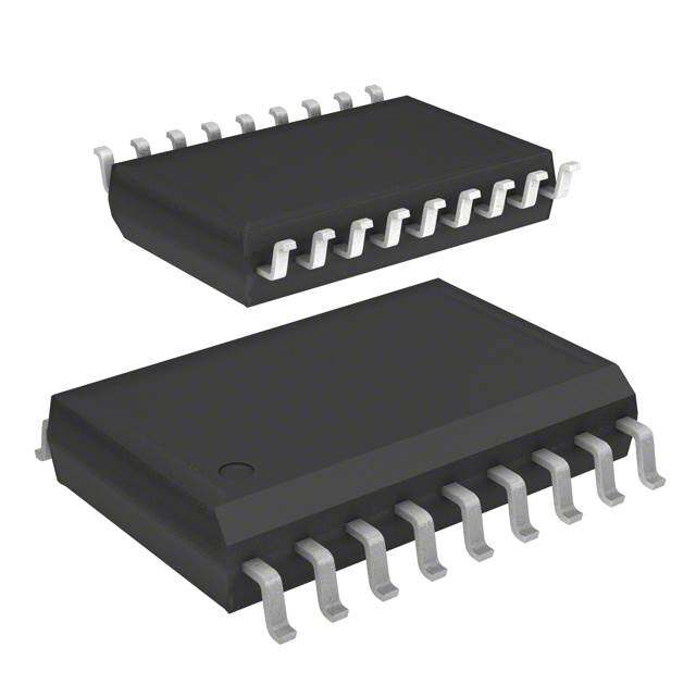
ICGOO电子元器件商城为您提供PCF2127AT/1,512由NXP Semiconductors设计生产,在icgoo商城现货销售,并且可以通过原厂、代理商等渠道进行代购。 PCF2127AT/1,512价格参考。NXP SemiconductorsPCF2127AT/1,512封装/规格:时钟/计时 - 实时时钟, Real Time Clock (RTC) IC Clock/Calendar 512B I²C, 2-Wire Serial 20-SOIC (0.295", 7.50mm Width)。您可以下载PCF2127AT/1,512参考资料、Datasheet数据手册功能说明书,资料中有PCF2127AT/1,512 详细功能的应用电路图电压和使用方法及教程。
| 参数 | 数值 |
| 产品目录 | 集成电路 (IC) |
| 描述 | IC RTC CLK/CAL I2C/SPI 20-SOIC |
| 产品分类 | |
| 品牌 | NXP Semiconductors |
| 数据手册 | |
| 产品图片 |
|
| 产品型号 | PCF2127AT/1,512 |
| PCN过时产品 | |
| rohs | 无铅 / 符合限制有害物质指令(RoHS)规范要求 |
| 产品系列 | - |
| 产品目录页面 | |
| 供应商器件封装 | 20-SO |
| 其它名称 | 568-4961-5 |
| 包装 | 管件 |
| 存储容量 | 512B |
| 安装类型 | 表面贴装 |
| 封装/外壳 | 20-SOIC(0.295",7.50mm 宽) |
| 工作温度 | -40°C ~ 85°C |
| 接口 | I²C,2 线串口,SPI |
| 日期格式 | YY-MM-DD-dd |
| 时间格式 | HH:MM:SS(12/24 小时) |
| 标准包装 | 38 |
| 特性 | 警报器,闰年,方波输出,SRAM,TCXO/晶体,监视计时器 |
| 特色产品 | http://www.digikey.com/cn/zh/ph/NXP/RTC.htmlhttp://www.digikey.com/cn/zh/ph/NXP/I2C.html |
| 电压-电源 | 1.8 V ~ 4.2 V |
| 电压-电源,电池 | 1.8 V ~ 4.2 V |
| 电流-计时(最大) | 1.5µA @ 3.3V |
| 类型 | 时钟/日历 |


- 商务部:美国ITC正式对集成电路等产品启动337调查
- 曝三星4nm工艺存在良率问题 高通将骁龙8 Gen1或转产台积电
- 太阳诱电将投资9.5亿元在常州建新厂生产MLCC 预计2023年完工
- 英特尔发布欧洲新工厂建设计划 深化IDM 2.0 战略
- 台积电先进制程称霸业界 有大客户加持明年业绩稳了
- 达到5530亿美元!SIA预计今年全球半导体销售额将创下新高
- 英特尔拟将自动驾驶子公司Mobileye上市 估值或超500亿美元
- 三星加码芯片和SET,合并消费电子和移动部门,撤换高东真等 CEO
- 三星电子宣布重大人事变动 还合并消费电子和移动部门
- 海关总署:前11个月进口集成电路产品价值2.52万亿元 增长14.8%


PDF Datasheet 数据手册内容提取
PCF2127AT Integrated RTC, TCXO and quartz crystal Rev. 6 — 11 July 2013 Product data sheet 1. General description The PCF2127AT1 is a CMOS2 Real Time Clock (RTC) and calendar with an integrated Temperature Compensated Crystal (Xtal) Oscillator (TCXO) and a 32.768kHz quartz crystal optimized for very high accuracy and very low power consumption. The PCF2127AT has 512bytes of general purpose static RAM, a selectable I2C-bus or SPI-bus, a backup battery switch-over circuit, a programmable watchdog function, a timestamp function, and many other features. 2. Features and benefits Temperature Compensated Crystal Oscillator (TCXO) with integrated capacitors Typical accuracy: 3ppm from 15 C to +60C Integration of a 32.768kHz quartz crystal and oscillator in the same package Provides year, month, day, weekday, hours, minutes, seconds, and leap year correction 512bytes of general purpose static RAM Timestamp function with interrupt capability detection of two different events on one multilevel input pin (for example, for tamper detection) Two line bidirectional 400kHz Fast-mode I2C-bus interface (I =3mA at pin OL SDA/CE) 3line SPI-bus with separate data input and output (maximum speed 6.5Mbit/s) Battery backup input pin and switch-over circuitry Battery backed output voltage Battery low detection function Extra power fail detection function with input and output pins Power-On Reset Override (PORO) Oscillator stop detection function Interrupt output and system reset pin (open-drain) Programmable 1second or 1minute interrupt Programmable countdown timer with interrupt capability Programmable watchdog timer with interrupt and reset capability Programmable alarm function with interrupt capability Programmable square wave open-drain output pin 1. As well as the PCF2129. 2. The definition of the abbreviations and acronyms used in this data sheet can be found in Section20.
PCF2127AT NXP Semiconductors Integrated RTC, TCXO and quartz crystal Clock operating voltage: 1.2V to 4.2V Low supply current: typical 0.65A at V =3.0V and T =25C DD amb 3. Applications Electronic metering for electricity, water, and gas Precision timekeeping Access to accurate time of the day GPS equipment to reduce time to first fix Applications that require an accurate process timing Products with long automated unattended operation time 4. Ordering information Table 1. Ordering information Type number Package Name Description Version PCF2127AT SO20 plastic small outline package; 20leads; body width 7.5mm SOT163-1 4.1 Ordering options Table 2. Ordering options Product type number IC Sales item (12NC) Delivery form revision PCF2127AT/1[1] 1 935290953512 tube, dry pack 935290953518 tape and reel, 13 inch, dry pack PCF2127AT/2 2 935299867518 tape and reel, 13 inch, dry pack [1] Not to be used for new designs. Replacement part is PCF2127AT/2. 5. Marking Table 3. Marking codes Product type number Marking code PCF2127AT/1 PCF2127AT PCF2127AT/2 PCF2127AT PCF2127AT All information provided in this document is subject to legal disclaimers. © NXP B.V. 2013. All rights reserved. Product data sheet Rev. 6 — 11 July 2013 2 of 86
PCF2127AT NXP Semiconductors Integrated RTC, TCXO and quartz crystal 6. Block diagram INT OSCI TCXO Control_1 00h DIVIDER 32.768 kHz OSCO AND Control_2 01h TIMER Control_3 02h CLKOUT Seconds 03h Minutes 04h BBS internal TEMP 1 Hz Hours 05h VDD BATTERY BACK UP power Days 06h supply VBAT SWITCH-OVER Weekdays 07h VSS CIRCUITRY COLONGTRICOL Months 08h Years 09h OSCILLATOR RESET Second_alarm 0Ah MONITOR Minute_alarm 0Bh RST Hour_alarm 0Ch SPI-BUS ADDRESS Day_alarm 0Dh INTERFACE REGISTER Weekday_alarm 0Eh CLKOUT_ctl 0Fh SDA/CE Watchdg_tim_ctl 10h SDO SERIAL BUS Watchdg_tim_val 11h INTERFACE SDI SELECTOR Timestp_ctl 12h SCL Sec_timestp 13h IFS Min_timestp 14h PCF2127AT I2C-BUS Hour_timestp 15h INTERFACE RPU Day_timestp 16h TS Mon_timestp 17h SCL Year_timestp 18h SDO 512 BYTES Aging_offset 19h SDI STATIC RAM RAM_addr_MSB 1Ah SDA/CE RAM_addr_LSB 1Bh RAM_wrt_cmd 1Ch PFI TEMP TEMPERATURE RAM_rd_cmd 1Dh SENSOR 1.25 V (internal) PFO TEST 001aaj675 Fig 1. Block diagram of PCF2127AT PCF2127AT All information provided in this document is subject to legal disclaimers. © NXP B.V. 2013. All rights reserved. Product data sheet Rev. 6 — 11 July 2013 3 of 86
PCF2127AT NXP Semiconductors Integrated RTC, TCXO and quartz crystal 7. Pinning information 7.1 Pinning SCL 1 20 VDD SDI 2 19 VBAT SDO 3 18 BBS SDA/CE 4 17 INT IFS 5 16 RST PCF2127AT TS 6 15 PFI CLKOUT 7 14 PFO VSS 8 13 TEST n.c. 9 12 n.c. n.c. 10 11 n.c. 001aaj676 Top view. For mechanical details, see Figure53. Fig 2. Pin configuration for SO20 (PCF2127AT) 7.2 Pin description Table 4. Pin description of SO20 (PCF2127AT) Symbol Pin Description SCL 1 combined serial clock input for both I2C-bus and SPI-bus SDI 2 serial data input for SPI-bus; connect to pin V if I2C-bus is selected SS SDO 3 serial data output for SPI-bus, push-pull SDA/CE 4 combined serial data input and output for the I2C-bus and chip enable input (active LOW) for the SPI-bus IFS 5 interface selector input connect to pin V to select the SPI-bus SS connect to pin BBS to select the I2C-bus TS 6 timestamp input (active LOW) with 200k internal pull-up resistor (R ) PU CLKOUT 7 clock output (open-drain) V 8 ground supply voltage SS n.c. 9 to 12 not connected; do not connect; do not use as feed through TEST 13 do not connect; do not use as feed through PFO 14 power fail output (open-drain; active LOW) PFI 15 power fail input RST 16 reset output (open-drain; active LOW) INT 17 interrupt output (open-drain; active LOW) PCF2127AT All information provided in this document is subject to legal disclaimers. © NXP B.V. 2013. All rights reserved. Product data sheet Rev. 6 — 11 July 2013 4 of 86
PCF2127AT NXP Semiconductors Integrated RTC, TCXO and quartz crystal Table 4. Pin description of SO20 (PCF2127AT) …continued Symbol Pin Description BBS 18 output voltage (battery backed) V 19 battery supply voltage (backup) BAT connect to V if battery switch over is not used SS V 20 supply voltage DD PCF2127AT All information provided in this document is subject to legal disclaimers. © NXP B.V. 2013. All rights reserved. Product data sheet Rev. 6 — 11 July 2013 5 of 86
PCF2127AT NXP Semiconductors Integrated RTC, TCXO and quartz crystal 8. Functional description The PCF2127AT is a Real Time Clock (RTC) and calendar with an on-chip Temperature Compensated Crystal (Xtal) Oscillator (TCXO) and a 32.768kHz quartz crystal integrated into the same package (see Section8.3.2). Address and data are transferred by a selectable 400kHz Fast-mode I2C-bus or a 3line SPI-bus with separate data input and output (see Section9). The maximum speed of the SPI-bus is 6.5Mbit/s. The PCF2127AT has a backup battery input pin and backup battery switch-over circuit which monitors the main power supply. The backup battery switch-over circuit automatically switches to the backup battery when a power failure condition is detected (see Section8.6.1). Accurate timekeeping is maintained even when the main power supply is interrupted. A battery low detection circuit monitors the status of the battery (see Section8.6.3). When the battery voltage drops below a certain threshold value, a flag is set to indicate that the battery must be replaced soon. This ensures the integrity of the data during periods of battery backup. 8.1 Register overview The PCF2127AT contains an auto-incrementing address register: the built-in address register will increment automatically after each read or write of a data byte up to the register 1Bh. After register 1Bh, the auto-incrementing will wrap around to address 00h (see Figure3). address register 00h 01h 02h auto-increment 03h ... 19h 1Ah wrap around 1Bh 1Ch not reachable by auto-inc. - needs to be addressed directly 1Dh not reachable by auto-inc. - needs to be addressed directly 001aaj307 Fig 3. Handling address registers • The first three registers (memory address 00h, 01h, and 02h) are used as control registers (see Section8.2). • The registers at addresses 03h through to 09h are used as counters for the clock function (seconds up to years). The date is automatically adjusted for months with fewer than 31days, including corrections for leap years. The clock can operate in 12-hour mode with an AM/PM indication or in 24-hour mode (see Section8.9). • The registers at addresses 0Ah through 0Eh define the alarm function. It can be selected that an interrupt is generated when an alarm event occurs (see Section8.10). PCF2127AT All information provided in this document is subject to legal disclaimers. © NXP B.V. 2013. All rights reserved. Product data sheet Rev. 6 — 11 July 2013 6 of 86
PCF2127AT NXP Semiconductors Integrated RTC, TCXO and quartz crystal • The register at address 0Fh defines the temperature measurement period and the clock out mode. The temperature measurement can be selected from every 4minutes (default) down to every 30seconds (see Table10). CLKOUT frequencies of 32.768kHz (default) down to 1Hz for use as system clock, microcontroller clock, and so on, can be chosen (see Table11). • The registers at addresses 10h and 11h are used for the watchdog and countdown timer functions. The watchdog timer has four selectable source clocks allowing for timer periods from less than 1ms to greater than 4hours (see Table37). Either the watchdog timer or the countdown timer can be enabled (see Section8.11). For the watchdog timer, it is possible to select whether an interrupt or a pulse on the reset pin will be generated when the watchdog times out. For the countdown timer, it is only possible that an interrupt will be generated at the end of the countdown. • The registers at addresses 12h to 18h are used for the timestamp function. When the trigger event happens, the actual time is saved in the timestamp registers (see Section8.12). • The register at address 19h is used for the correction of the crystal aging effect (see Section8.4.1). • The registers at addresses 1Ah and 1Bh define the RAM address. The register at address 1Ch (RAM_wrt_cmd) is the RAM write command; the register at 1Dh (RAM_rd_cmd) is the RAM read command. Data is transferred to or from the RAM by the serial interface (see Section8.5). • The registers Seconds, Minutes, Hours, Days, Months, and Years are all coded in Binary Coded Decimal (BCD) format to simplify application use. Other registers are either bit-wise or standard binary. When one of the RTC registers is written or read, the content of all counters is temporarily frozen. This prevents a faulty writing or reading of the clock and calendar during a carry condition (see Section8.9.8). PCF2127AT All information provided in this document is subject to legal disclaimers. © NXP B.V. 2013. All rights reserved. Product data sheet Rev. 6 — 11 July 2013 7 of 86
PCF2127AT NXP Semiconductors Integrated RTC, TCXO and quartz crystal Table 5. Register ove rview Bit positions labeled as- are not implemented and will return a 0 when read. Bit T must always be written with logic0. Bits labeled as X are undefined at power-on and unchanged by subsequent resets. Address Register name Bit Reset value 7 6 5 4 3 2 1 0 Control registers 00h Control_1 EXT_ T STOP TSF1 POR_ 12_24 MI SI 0000 0000 TEST OVRD 01h Control_2 MSF WDTF TSF2 AF CDTF TSIE AIE CDTIE 0000 0000 02h Control_3 PWRMNG[2:0] BTSE BF BLF BIE BLIE 0000 0000 Time and date registers 03h Seconds OSF SECONDS (0 to 59) 1XXX XXXX 04h Minutes - MINUTES (0 to 59) -XXX XXXX 05h Hours - - AMPM HOURS (1 to 12) in 12h mode --XX XXXX HOURS (0 to 23) in 24h mode --XX XXXX 06h Days - - DAYS (1 to 31) --XX XXXX 07h Weekdays - - - - - WEEKDAYS (0 to 6) ---- -XXX 08h Months - - - MONTHS (1 to 12) ---X XXXX 09h Years YEARS (0 to 99) XXXX XXXX Alarm registers 0Ah Second_alarm AE_S SECOND_ALARM (0 to 59) 1XXX XXXX 0Bh Minute_alarm AE_M MINUTE_ALARM (0 to 59) 1XXX XXXX 0Ch Hour_alarm AE_H - AMPM HOUR_ALARM (1 to 12) in 12h mode 1-XX XXXX - HOUR_ALARM (0 to 23) in 24h mode 1-XX XXXX 0Dh Day_alarm AE_D - DAY_ALARM (1 to 31) 1-XX XXXX 0Eh Weekday_alarm AE_W - - - - WEEKDAY_ALARM (0 to 6) 1--- -XXX CLKOUT control register 0Fh CLKOUT_ctl TCR[1:0] - - - COF[2:0] 00-- -000 Watchdog registers 10h Watchdg_tim_ctl WD_CD[1:0] TI_TP - - - TF[1:0] 000- --11 11h Watchdg_tim_val WATCHDG_TIM_VAL[7:0] XXXX XXXX Timestamp registers 12h Timestp_ctl TSM TSOFF - 1_O_16_TIMESTP[4:0] 00-X XXXX 13h Sec_timestp - SECOND_TIMESTP (0 to 59) -XXX XXXX 14h Min_timestp - MINUTE_TIMESTP (0 to 59) -XXX XXXX 15h Hour_timestp - - AMPM HOUR_TIMESTP (1 to 12) in 12h mode --XX XXXX HOUR_TIMESTP (0 to 23) in 24h mode --XX XXXX 16h Day_timestp - - DAY_TIMESTP (1 to 31) --XX XXXX 17h Mon_timestp - - - MONTH_TIMESTP (1 to 12) ---X XXXX 18h Year_timestp YEAR_TIMESTP (0 to 99) XXXX XXXX Aging offset register 19h Aging_offset - - - - AO[3:0] ---- 1000 PCF2127AT All information provided in this document is subject to legal disclaimers. © NXP B.V. 2013. All rights reserved. Product data sheet Rev. 6 — 11 July 2013 8 of 86
PCF2127AT NXP Semiconductors Integrated RTC, TCXO and quartz crystal Table 5. Register overview …continued Bit positions labeled as- are not implemented and will return a 0 when read. Bit T must always be written with logic0. Bits labeled as X are undefined at power-on and unchanged by subsequent resets. Address Register name Bit Reset value 7 6 5 4 3 2 1 0 RAM registers 1Ah RAM_addr_MSB - - - - - - - RA8 ---- ---0 1Bh RAM_addr_LSB RA[7:0] 0000 0000 1Ch RAM_wrt_cmd X X X X X X X X XXXX XXXX 1Dh RAM_rd_cmd X X X X X X X X XXXX XXXX PCF2127AT All information provided in this document is subject to legal disclaimers. © NXP B.V. 2013. All rights reserved. Product data sheet Rev. 6 — 11 July 2013 9 of 86
PCF2127AT NXP Semiconductors Integrated RTC, TCXO and quartz crystal 8.2 Control registers The first 3 registers of the PCF2127AT, with the addresses 00h, 01h, and 02h, are used as control registers. 8.2.1 Register Control_1 Table 6. Control_1 - control and status register 1 (address 00h) bit description Bit Symbol Value Description Reference 7 EXT_TEST 0 [1] normal mode Section8.14 1 external clock test mode 6 T 0 [2] unused - 5 STOP 0 [1] RTC source clock runs Section8.15 1 RTC clock is stopped; RTC divider chain flip-flops are asynchronously set logic0; CLKOUT at 32.768kHz, 16.384kHz, or 8.192kHz is still available 4 TSF1 0 [1] no timestamp interrupt generated Section8.12.1 1 flag set when TS input is driven to an intermediate level between power supply and ground; flag must be cleared to clear interrupt 3 POR_OVRD 0 [1] Power-On Reset Override (PORO) facility Section8.8.2 disabled; set logic0 for normal operation 1 Power-On Reset Override (PORO) sequence reception enabled 2 12_24 0 [1] 24hour mode selected Table23 1 12hour mode selected 1 MI 0 [1] minute interrupt disabled Section8.13 1 minute interrupt enabled 0 SI 0 [1] second interrupt disabled 1 second interrupt enabled [1] Default value. [2] When writing to the register this bit always has to be set logic 0. PCF2127AT All information provided in this document is subject to legal disclaimers. © NXP B.V. 2013. All rights reserved. Product data sheet Rev. 6 — 11 July 2013 10 of 86
PCF2127AT NXP Semiconductors Integrated RTC, TCXO and quartz crystal 8.2.2 Register Control_2 Table 7. Control_2 - control and status register 2 (address 01h) bit description Bit Symbol Value Description Reference 7 MSF 0 [1] no minute or second interrupt generated Section8.13 1 flag set when minute or second interrupt generated; flag must be cleared to clear interrupt 6 WDTF 0 [1] no watchdog timer interrupt or reset Section8.13.4 generated 1 flag set when watchdog timer interrupt or reset generated; flag cannot be cleared by command (read-only) 5 TSF2 0 [1] no timestamp interrupt generated Section8.12.1 1 flag set when TS input is driven to ground; flag must be cleared to clear interrupt 4 AF 0 [1] no alarm interrupt generated Section8.10.6 1 flag set when alarm triggered; flag must be cleared to clear interrupt 3 CDTF 0 [1] no countdown timer interrupt generated Section8.11.4 1 flag set when countdown timer interrupt generated; flag must be cleared to clear interrupt 2 TSIE 0 [1] no interrupt generated from timestamp flag Section8.13.6 1 interrupt generated when timestamp flag set 1 AIE 0 [1] no interrupt generated from the alarm flag Section8.13.5 1 interrupt generated when alarm flag set 0 CDTIE 0 [1] no interrupt generated from countdown timer Section8.13.2 flag 1 interrupt generated when countdown timer flag set [1] Default value. PCF2127AT All information provided in this document is subject to legal disclaimers. © NXP B.V. 2013. All rights reserved. Product data sheet Rev. 6 — 11 July 2013 11 of 86
PCF2127AT NXP Semiconductors Integrated RTC, TCXO and quartz crystal 8.2.3 Register Control_3 Table 8. Control_3 - control and status register 3 (address 02h) bit description Bit Symbol Value Description Reference 7 to 5 PWRMNG[2:0] [1] control of the battery switch-over, battery low Section8.6 detection, and extra power fail detection functions 4 BTSE 0 [2] no timestamp when battery switch-over Section8.12.4 occurs 1 time-stamped when battery switch-over occurs 3 BF 0 [2] no battery switch-over interrupt generated Section8.6.1 1 flag set when battery switch-over occurs; flag must be cleared to clear interrupt 2 BLF 0 [2] battery status ok; Section8.6.3 no battery low interrupt generated 1 battery status low; flag cannot be cleared by command 1 BIE 0 [2] no interrupt generated from the battery flag Section8.13.7 (BF) 1 interrupt generated when BF is set 0 BLIE 0 [2] no interrupt generated from battery low flag Section8.13.8 (BLF) 1 interrupt generated when BLF is set [1] Values see Table18. [2] Default value. PCF2127AT All information provided in this document is subject to legal disclaimers. © NXP B.V. 2013. All rights reserved. Product data sheet Rev. 6 — 11 July 2013 12 of 86
PCF2127AT NXP Semiconductors Integrated RTC, TCXO and quartz crystal 8.3 Register CLKOUT_ctl Table 9. CLKOUT_ctl - CLKOUT control register (address 0Fh) bit description Bit Symbol Value Description 7 to 6 TCR[1:0] see Table10 temperature measurement period 5to3 - - unused 2to0 COF[2:0] see Table11 CLKOUT frequency selection 8.3.1 Temperature compensated crystal oscillator The frequency of tuning fork quartz crystal oscillators is temperature-dependent. In the PCF2127AT, the frequency deviation caused by temperature variation is corrected by adjusting the load capacitance of the crystal oscillator. The load capacitance is changed by switching between two load capacitance values using a modulation signal with a programmable duty cycle. In order to compensate the spread of the quartz parameters every chip is factory calibrated. The frequency accuracy can be evaluated by measuring the frequency of the square wave signal available at the output pin CLKOUT. However, the selection of f =32.768kHz (default value) leads to inaccurate measurements. Accurate CLKOUT frequency measurement occurs when f =16.384kHz or lower is selected (see CLKOUT Table11). 8.3.1.1 Temperature measurement The PCF2127AT has a temperature sensor circuit used to perform the temperature compensation of the frequency. The temperature is measured immediately after power-on and then periodically with a period set by the temperature conversion rate TCR[1:0] in the register CLKOUT_ctl. Table 10. Temperature measurement period TCR[1:0] Temperature measurement period 00 [1] 4min 01 2min 10 1min 11 30seconds [1] Default value. 8.3.2 Clock output A programmable square wave is available at pinCLKOUT. Operation is controlled by the COF[2:0] control bits in register CLKOUT_ctl. Frequencies of 32.768kHz (default) down to 1Hz can be generated for use as system clock, microcontroller clock, charge pump input, or for calibrating the oscillator. CLKOUT is an open-drain output and enabled at power-on. When disabled, the output is high-impedance. The duty cycle of the selected clock is not controlled, however, due to the nature of the clock generation all but the 32.768kHz frequencies will be 50:50. PCF2127AT All information provided in this document is subject to legal disclaimers. © NXP B.V. 2013. All rights reserved. Product data sheet Rev. 6 — 11 July 2013 13 of 86
PCF2127AT NXP Semiconductors Integrated RTC, TCXO and quartz crystal Table 11. CLKOUT frequency selection COF[2:0] CLKOUT frequency (Hz) Typical duty cycle[1] 000[2][3] 32768 60:40 to 40:60 001 16384 50:50 010 8192 50:50 011 4096 50:50 100 2048 50:50 101 1024 50:50 110 1 50:50 111 CLKOUT = high-Z - [1] Duty cycle definition: %HIGH-level time: %LOW-level time. [2] Default value. [3] The specified accuracy of the RTC can be only achieved with CLKOUT frequencies not equal to 32.768kHz or if CLKOUT is disabled. PCF2127AT All information provided in this document is subject to legal disclaimers. © NXP B.V. 2013. All rights reserved. Product data sheet Rev. 6 — 11 July 2013 14 of 86
PCF2127AT NXP Semiconductors Integrated RTC, TCXO and quartz crystal 8.4 Register Aging_offset Table 12. Aging_offset - crystal aging offset register (address 19h) bit description Bit Symbol Value Description 7 to 4 - - unused 3 to 0 AO[3:0] see Table13 aging offset value 8.4.1 Crystal aging correction The PCF2127AT has an offset register Aging_offset to correct the crystal aging effects3. The accuracy of the frequency of a quartz crystal depends on its aging. The aging offset adds an adjustment, positive or negative, in the temperature compensation circuit which allows correcting the aging effect. At 25 C, the aging offset bits allow a frequency correction of typically 1ppm per AO[3:0] value, from 7ppm to +8ppm. Table 13. Frequency correction at 25C, typical AO[3:0] ppm Decimal Binary 0 0000 +8 1 0001 +7 2 0010 +6 3 0011 +5 4 0100 +4 5 0101 +3 6 0110 +2 7 0111 +1 8 1000 [1] 0 9 1001 1 10 1010 2 11 1011 3 12 1100 4 13 1101 5 14 1110 6 15 1111 7 [1] Default value. 3. For further information, refer to the application note Ref. 3 “AN10857”. PCF2127AT All information provided in this document is subject to legal disclaimers. © NXP B.V. 2013. All rights reserved. Product data sheet Rev. 6 — 11 July 2013 15 of 86
PCF2127AT NXP Semiconductors Integrated RTC, TCXO and quartz crystal 8.5 General purpose 512 bytes static RAM The PCF2127AT contains a general purpose 512bytes static RAM. This integrated SRAM is battery backed and can therefore be used to store data which is essential for the application to survive a power outage. 9bits, RA[8:0], define the RAM address pointer in registers RAM_addr_MSB and RAM_addr_LSB. The register address pointer increments after each read or write automatically up to 1Bh and then wraps around to address 00h (see Figure3 on page6). Data is transferred to or from the RAM by the interface. To write to the RAM, the register RAM_wrt_cmd, to read from the RAM the register RAM_rd_cmd must be addressed explicitly. 8.5.1 Register RAM_addr_MSB Table 14. RAM_addr_MSB - RAM address MSB register (address 1Ah) bit description Bit Symbol Description 7 to 1 - unused 0 RA8 RAM address, MSB (9th bit) 8.5.2 Register RAM_addr_LSB Table 15. RAM_addr_LSB - RAM address LSB register (address 1Bh) bit description Bit Symbol Description 7 to 0 RA[7:0] RAM address, LSB (1st to 8th bit) 8.5.3 Register RAM_wrt_cmd Table 16. RAM_wrt_cmd - RAM write command register (address 1Ch) bit description Bit Symbol Description 7 to 0 - data to be written into RAM 8.5.4 Register RAM_rd_cmd Table 17. RAM_rd_cmd - RAM read command register (address 1Dh) bit description Bit Symbol Description 7 to 0 - data to be read from RAM PCF2127AT All information provided in this document is subject to legal disclaimers. © NXP B.V. 2013. All rights reserved. Product data sheet Rev. 6 — 11 July 2013 16 of 86
PCF2127AT NXP Semiconductors Integrated RTC, TCXO and quartz crystal 8.5.5 Operation examples 8.5.5.1 Writing to the RAM 1. Set RAM address: – Select register RAM_addr_MSB (send address 1Ah). – Set value for bit RA8 (data byte of register 1Ah). Note: register address will be incremented automatically to 1Bh. – Set value for array RA[7:0] (data byte of register 1Bh). 2. Send RAM write command: – Select register RAM_wrt_cmd (send address 1Ch). 3. Write data into the RAM: – Write n data byte into RAM. For details, see Figure44 on page62. 8.5.5.2 Reading from the RAM 1. Set RAM address: – Select register RAM_addr_MSB (send address 1Ah). – Set value for bit RA8 (data byte of register 1Ah). Note: register address will be incremented automatically to 1Bh. – Set value for array RA[7:0] (data byte of register 1Bh). 2. Send RAM read command: – Select register RAM_rd_cmd (send address 1Dh). 3. Read from the RAM: – Read n data byte from the RAM. For details, see Figure45 on page63. PCF2127AT All information provided in this document is subject to legal disclaimers. © NXP B.V. 2013. All rights reserved. Product data sheet Rev. 6 — 11 July 2013 17 of 86
PCF2127AT NXP Semiconductors Integrated RTC, TCXO and quartz crystal 8.6 Power management functions The PCF2127AT has two power supply pins and one power output pin: • V - the main power supply input pin DD • V - the battery backup input pin BAT • BBS - battery backed output voltage pin (equal to the internal power supply) The PCF2127AT has three power management functions implemented: • Battery switch-over function • Battery low detection function • Extra power fail detection function The power management functions are controlled by the control bits PWRMNG[2:0] in register Control_3: Table 18. Power management control bit description PWRMNG[2:0] Function 000 [1] battery switch-over function is enabled in standard mode; battery low detection function is enabled; extra power fail detection function is enabled 001 battery switch-over function is enabled in standard mode; battery low detection function is disabled; extra power fail detection function is enabled 010 battery switch-over function is enabled in standard mode; battery low detection function is disabled; extra power fail detection function is disabled 011 battery switch-over function is enabled in direct switching mode; battery low detection function is enabled; extra power fail detection function is enabled 100 battery switch-over function is enabled in direct switching mode; battery low detection function is disabled; extra power fail detection function is enabled 101 battery switch-over function is enabled in direct switching mode; battery low detection function is disabled; extra power fail detection function is disabled 110 [2] battery switch-over function is disabled - only one power supply (V ); DD battery low detection function is disabled; extra power fail detection function is enabled 111 [2] battery switch-over function is disabled - only one power supply (V ); DD battery low detection function is disabled; extra power fail detection function is disabled [1] Default value. [2] When the battery switch-over function is disabled, the PCF2127AT works only with the power supply V ; DD V must be put to ground and the battery low detection function is disabled. BAT PCF2127AT All information provided in this document is subject to legal disclaimers. © NXP B.V. 2013. All rights reserved. Product data sheet Rev. 6 — 11 July 2013 18 of 86
PCF2127AT NXP Semiconductors Integrated RTC, TCXO and quartz crystal 8.6.1 Battery switch-over function The PCF2127AT has a backup battery switch-over circuit which monitors the main power supply V . When a power failure condition is detected, it automatically switches to the DD backup battery. One of two operation modes can be selected: • Standard mode: the power failure condition happens when: V < V AND V <V DD BAT DD th(sw)bat V is the battery switch threshold voltage. Typical value is 2.5V. The battery th(sw)bat switch-over in standard mode works only for V > 2.5V. DD • Direct switching mode: the power failure condition happens when V < V . DD BAT Direct switching from V to V without requiring V to drop below V DD BAT DD th(sw)bat When a power failure condition occurs and the power supply switches to the battery, the following sequence occurs: 1. The battery switch flag BF (register Control_3) is set logic 1. 2. An interrupt is generated if the control bit BIE (register Control_3) is enabled (seeSection8.13.7). 3. If the control bit BTSE (register Control_3) is logic 1, the timestamp registers store the time and date when the battery switch occurred (see Section8.12.4). 4. The battery switch flag BF is cleared by command; it must be cleared to clear the interrupt. The interface is disabled in battery backup operation: • Interface inputs are not recognized, preventing extraneous data being written to the device • Interface outputs are high-impedance PCF2127AT All information provided in this document is subject to legal disclaimers. © NXP B.V. 2013. All rights reserved. Product data sheet Rev. 6 — 11 July 2013 19 of 86
PCF2127AT NXP Semiconductors Integrated RTC, TCXO and quartz crystal 8.6.1.1 Standard mode If V > V OR V >V , the internal power supply is V . DD BAT DD th(sw)bat DD If V < V AND V <V , the internal power supply is V . DD BAT DD th(sw)bat BAT backup battery operation VDD VBBS VBBS VBAT internal power supply (= VBBS) Vth(sw)bat (= 2.5 V) VDD (= 0 V) BF INT cleared via interface 001aaj311 V is the battery switch threshold voltage. Typical value is 2.5V. In standard mode, the th(sw)bat battery switch-over works only for VDD > 2.5V. V may be lower than V (for example V =3V, V =4.1V). DD BAT DD BAT Fig 4. Battery switch-over behavior in standard mode with bit BIE set logic 1 (enabled) PCF2127AT All information provided in this document is subject to legal disclaimers. © NXP B.V. 2013. All rights reserved. Product data sheet Rev. 6 — 11 July 2013 20 of 86
PCF2127AT NXP Semiconductors Integrated RTC, TCXO and quartz crystal 8.6.1.2 Direct switching mode If V > V the internal power supply is V . DD BAT, DD If V < V , the internal power supply is V . DD BAT BAT The direct switching mode is useful in systems where V is higher than V at all times. DD BAT This mode is not recommended if the V and V values are similar (for example, DD BAT V =3.3V, V 3.0V). In direct switching mode, the power consumption is reduced DD BAT compared to the standard mode because the monitoring of V and V is not DD th(sw)bat performed. backup battery operation VDD VBBS VBBS VBAT internal power supply (= VBBS) Vth(sw)bat (= 2.5 V) VDD (= 0 V) BF INT cleared via interface 001aaj312 Fig 5. Battery switch-over behavior in direct switching mode with bit BIE set logic 1 (enabled) 8.6.1.3 Battery switch-over disabled: only one power supply (V ) DD When the battery switch-over function is disabled: • The power supply is applied on the V pin DD • The V pin must be connected to ground BAT • The internal power supply, available at the output pin BBS, is equal to V DD • The battery flag (BF) is always logic 0 PCF2127AT All information provided in this document is subject to legal disclaimers. © NXP B.V. 2013. All rights reserved. Product data sheet Rev. 6 — 11 July 2013 21 of 86
PCF2127AT NXP Semiconductors Integrated RTC, TCXO and quartz crystal 8.6.1.4 Battery switch-over architecture The architecture of the battery switch-over circuit is shown in Figure6. comparators logic switches VDD(int) VCC Vth(sw)bat VDD VDD VDD(int) VCC LOGIC VBBS (internal Vth(sw)bat power supply) VBAT VBAT 001aag061 VDD(int) Fig 6. Battery switch-over circuit, simplified block diagram The internal power supply (available on pin BBS) is equal to V or V . It has to be DD BAT assured that there are decoupling capacitors on the pins V , V , and BBS. DD BAT 8.6.2 Battery backup supply The V voltage on the output pin BBS is equal to the internal power supply, depending BBS on the selected battery switch-over function mode: Table 19. Output pin BBS Battery switch-over function mode Conditions V equals BBS standard V > V OR V > V V DD BAT DD th(sw)bat DD V < V AND V < V V DD BAT DD th(sw)bat BAT direct switching V > V V DD BAT DD V < V V DD BAT BAT disabled only V available, V DD DD V must be put to ground BAT The output pin BBS can be used as a supply for external devices with battery backup needs, such as SRAM (see Ref. 3 “AN10857”). For this case, Figure7 shows the typical driving capability when V is driven from V . BBS DD PCF2127AT All information provided in this document is subject to legal disclaimers. © NXP B.V. 2013. All rights reserved. Product data sheet Rev. 6 — 11 July 2013 22 of 86
PCF2127AT NXP Semiconductors Integrated RTC, TCXO and quartz crystal 001aaj327 0 VBBS − VDD (mV) −200 VDD = 4.2 V −400 VDD = 3 V −600 VDD = 2 V −800 0 2 4 6 8 IBBS (mA) Fig 7. Typical driving capability of V : (V V ) with respect to the output load BBS BBS DD current I BBS 8.6.3 Battery low detection function The PCF2127AT has a battery low detection circuit which monitors the status of the battery V . BAT When V drops below the threshold value V (typically 2.5V), the BLF flag BAT th(bat)low (register Control_3) is set to indicate that the battery is low and that it must be replaced. Monitoring of the battery voltage also occurs during battery operation. An unreliable battery cannot prevent that the supply voltage drops below V (typical low 1.2V) and with that the data integrity gets lost. When V drops below the threshold value V , the following sequence occurs (see BAT th(bat)low Figure8): 1. The battery low flag BLF is set logic 1. 2. An interrupt is generated if the control bit BLIE (register Control_3) is enabled (seeSection8.13.8). 3. The flag BLF remains logic1 until the battery is replaced. BLF cannot be cleared by command. It is cleared automatically by the battery low detection circuit when the battery is replaced. PCF2127AT All information provided in this document is subject to legal disclaimers. © NXP B.V. 2013. All rights reserved. Product data sheet Rev. 6 — 11 July 2013 23 of 86
PCF2127AT NXP Semiconductors Integrated RTC, TCXO and quartz crystal VDD = VBBS internal power supply (= VBBS) VBAT Vth(bat)low (= 2.5 V) VBAT BLF INT 001aaj322 Fig 8. Battery low detection behavior with bit BLIE set logic 1 (enabled) 8.6.4 Extra power fail detection function The PCF2127AT has an extra power fail detection circuit which compares the voltage at the power fail input pin PFI to an internal reference voltage equal to 1.25V. If V < 1.25V, the power fail output PFO is driven LOW. PFO is an open-drain, active PFI LOW output which requires an external pull-up resistor in any application. The extra power fail detection function is typically used as a low voltage detection for the main power supply V (see Figure9). DD VDD PCF2127AT R1 RPU 1.25 V (internal) 15 PFI 14 PFO R2 VSS 001aaj678 Fig 9. Typical application of the extra power fail detection function Usually R1 and R2 should be chosen such that the voltage at pin PFI • is higher than 1.25V at start-up • falls below 1.25V when V falls below a desired threshold voltage, V , defined DD th(uvp) by Equation1: PCF2127AT All information provided in this document is subject to legal disclaimers. © NXP B.V. 2013. All rights reserved. Product data sheet Rev. 6 — 11 July 2013 24 of 86
PCF2127AT NXP Semiconductors Integrated RTC, TCXO and quartz crystal R V = ----1--+1 1.25V (1) thuvp R 2 V value is usually set to a value that there are several milliseconds before V falls th(uvp) DD below the minimum operating voltage of the system, in order to allow the microcontroller to perform early backup operations. If the extra power fail detection function is not used, pin PFI must be connected to V and SS pin PFO must be left open circuit. 8.6.4.1 Extra power fail detection when the battery switch over function is enabled • When the power switches to the backup battery supply V , the power fail BAT comparator is switched off and the power fail output at pin PFO goes (or remains) LOW • When the power switches back to the main V , the pin PFO is not driven LOW DD anymore and is pulled HIGH through the external pull-up resistance for a certain time (t = 15.63ms to 31.25ms) and then the power fail comparator is enabled again rec For illustration, see Figure10 and Figure11. VDD Vth(uvp) VBAT internal power supply (= VBBS) VBBS VBBS Vth(sw)bat (= 2.5 V) VDD (= 0 V) comparator comparator comparator enabled disabled enabled PF0 trec = [15.63 : 31.25] ms 001aaj319 Fig 10. PFO signal behavior when battery switch-over is enabled in standard mode and V >(V ,V ) th(uvp) BAT th(sw)bat PCF2127AT All information provided in this document is subject to legal disclaimers. © NXP B.V. 2013. All rights reserved. Product data sheet Rev. 6 — 11 July 2013 25 of 86
PCF2127AT NXP Semiconductors Integrated RTC, TCXO and quartz crystal VDD VBBS internal power supply (= VBBS) VBBS VBAT Vth(uvp) Vth(sw)bat (= 2.5 V) VDD (= 0 V) comparator comparator comparator enabled disabled enabled PF0 trec 001aaj320 Fig 11. PFO signal behavior when battery switch-over is enabled in direct switching mode and V < V th(uvp) BAT 8.6.4.2 Extra power fail detection when the battery switch-over function is disabled If the battery switch-over function is disabled and the power fail comparator is enabled, the power fail output at pin PFO depends only on the result of the comparison between V and 1.25V: PFI • If V > 1.25V, PFO = HIGH (through the external pull-up resistor) PFI • If V < 1.25V, PFO = LOW PFI VDD Vth(uvp) Vth(sw)bat (= 2.5 V) comparator always enabled PF0 001aaj321 Fig 12. PFO signal behavior when battery switch-over is disabled PCF2127AT All information provided in this document is subject to legal disclaimers. © NXP B.V. 2013. All rights reserved. Product data sheet Rev. 6 — 11 July 2013 26 of 86
PCF2127AT NXP Semiconductors Integrated RTC, TCXO and quartz crystal 8.7 Oscillator stop detection function The PCF2127AT has an on-chip oscillator detection circuit which monitors the status of the oscillation: whenever the oscillation stops, a reset occurs and the oscillator stop flag OSF (in register Seconds) is set logic 1. • Power-on: a. The oscillator is not running, the chip is in reset (pin RST is LOW and flag OSFis logic 1). b. When the oscillator starts running and is stable after power-on, the chip exits from reset (pin RSTisHIGH). c. The flag OSF is still logic1 and can be cleared (OSFset logic0) by command. • Power supply failure: a. When the power supply of the chip (V , see Section8.6.2) drops below a certain BBS value (V ), typically 1.2V, the oscillator stops running and a reset occurs. low b. When the power supply returns to normal operation, the oscillator starts running again, the chip exits from reset. c. The flag OSF is still logic1 and can be cleared (OSFset logic0) by command. VDD VDD VBBS VBAT VBBS VBBS Vth(sw)bat (= 2.5 V) VBBS battery discharge internal power supply Vlow (= 1.2 V) VBAT VSS VSS (1) (2) OSF 001aaj409 (1) Theoretical state of the signals since there is no power. (2) The oscillator stop flag (OSF), set logic 1, indicates that the oscillation has stopped and a reset has occurred since the flag was last cleared (OSF set logic 0). In this case, the integrity of the clock information is not guaranteed. The OSF flag is cleared by command. Fig 13. Power failure event due to battery discharge: reset occurs PCF2127AT All information provided in this document is subject to legal disclaimers. © NXP B.V. 2013. All rights reserved. Product data sheet Rev. 6 — 11 July 2013 27 of 86
PCF2127AT NXP Semiconductors Integrated RTC, TCXO and quartz crystal 8.8 Reset function The PCF2127AT has a Power-On Reset (POR) and a Power-On Reset Override (PORO) function implemented. 8.8.1 Power-On Reset (POR) The POR is active whenever the oscillator is stopped. The oscillator is also considered to be stopped during the time between power-on and stable crystal resonance (see Figure14). This time may be in the range of 200ms to 2s depending on temperature and supply voltage. Whenever an internal reset occurs, the oscillator stop flag is set (OSFset logic1). chip in reset chip not in reset VDD oscillation RST t 013aaa243 Fig 14. Dependency between POR and oscillator After POR, the following mode is entered: • 32.768kHz CLKOUT active • Power-On Reset Override (PORO) available to be set • 24hour mode is selected • Battery switch-over is enabled • Battery low detection is enabled • Extra power fail detection is enabled The register values after power-on are shown in Table5. 8.8.2 Power-On Reset Override (PORO) The POR duration is directly related to the crystal oscillator start-up time. Due to the long start-up times experienced by these types of circuits, a mechanism has been built in to disable the POR and therefore speed up the on-board test of the device. PCF2127AT All information provided in this document is subject to legal disclaimers. © NXP B.V. 2013. All rights reserved. Product data sheet Rev. 6 — 11 July 2013 28 of 86
PCF2127AT NXP Semiconductors Integrated RTC, TCXO and quartz crystal osc stopped OSCILLATOR 0 = stopped, 1 = running reset SCL RESET OVERRIDE 0 = override inactive 1 = override active SDA/CE CLEAR 0 = clear override mode POR_OVRD 1 = override possible 001aaj324 Fig 15. Power-On Reset (POR) system The setting of the PORO mode requires that POR_OVRD in register Control_1 is set logic1 and that the signals at the interface pins SDA/CE and SCL are toggled as illustrated in Figure16. All timings shown are required minimum. power up 8 ms minimum 500 ns minimum 2000 ns SDA/CE SCL reset override 001aaj326 Fig 16. Power-On Reset Override (PORO) sequence, valid for both I2C-bus and SPI-bus Once the override mode is entered, the device is immediately released from the reset state and the set-up operation can commence. The PORO mode is cleared by writing logic0 to POR_OVRD. POR_OVRD must be logic1 before a re-entry into the override mode is possible. Setting POR_OVRD logic0 during normal operation has no effect except to prevent accidental entry into the PORO mode. PCF2127AT All information provided in this document is subject to legal disclaimers. © NXP B.V. 2013. All rights reserved. Product data sheet Rev. 6 — 11 July 2013 29 of 86
PCF2127AT NXP Semiconductors Integrated RTC, TCXO and quartz crystal 8.9 Time and date function Most of these registers are coded in the Binary Coded Decimal (BCD) format. 8.9.1 Register Seconds Table 20. Seconds - seconds and clock integrity register (address 03h) bit description Bit Symbol Value Place value Description 7 OSF 0 - clock integrity is guaranteed 1[1] - clock integrity is not guaranteed: oscillator has stopped and chip reset has occurred since flag was last cleared 6to4 SECONDS 0to5 ten’s place actual seconds coded in BCD format 3to0 0to9 unit place [1] Start-up value. Table 21. Seconds coded in BCD format Seconds value in Upper-digit (ten’s place) Digit (unit place) decimal Bit6 Bit5 Bit4 Bit3 Bit2 Bit1 Bit0 00 0 0 0 0 0 0 0 01 0 0 0 0 0 0 1 02 0 0 0 0 0 1 0 : : : : : : : : 09 0 0 0 1 0 0 1 10 0 0 1 0 0 0 0 : : : : : : : : 58 1 0 1 1 0 0 0 59 1 0 1 1 0 0 1 8.9.2 Register Minutes Table 22. Minutes - minutes register (address 04h) bit description Bit Symbol Value Place value Description 7 - - - unused 6to4 MINUTES 0to5 ten’s place actual minutes coded in BCD format 3to0 0to9 unit place PCF2127AT All information provided in this document is subject to legal disclaimers. © NXP B.V. 2013. All rights reserved. Product data sheet Rev. 6 — 11 July 2013 30 of 86
PCF2127AT NXP Semiconductors Integrated RTC, TCXO and quartz crystal 8.9.3 Register Hours Table 23. Hours - hours register (address 05h) bit description Bit Symbol Value Place value Description 7to6 - - - unused 12 hour mode[1] 5 AMPM 0 - indicates AM 1 - indicates PM 4 HOURS 0to1 ten’s place actual hours coded in BCD format when in 12 hour mode 3to0 0to9 unit place 24 hour mode[1] 5to4 HOURS 0to2 ten’s place actual hours coded in BCD format when in 24 hour mode 3to0 0to9 unit place [1] Hour mode is set by the bit 12_24 in register Control_1. 8.9.4 Register Days Table 24. Days - days register (address 06h) bit description Bit Symbol Value Place value Description 7to6 - - - unused 5to4 DAYS[1] 0to3 ten’s place actual day coded in BCD format 3to0 0to9 unit place [1] If the year counter contains a value which is exactly divisible by4, including the year00, the RTC compensates for leap years by adding a 29th day to February. 8.9.5 Register Weekdays Table 25. Weekdays - weekdays register (address 07h) bit description Bit Symbol Value Description 7to3 - - unused 2to0 WEEKDAYS 0to6 actual weekday value, see Table26 Although the association of the weekdays counter to the actual weekday is arbitrary, the PCF2127AT will assume that Sunday is 000 and Monday is 001 for the purposes of determining the increment for calendar weeks. Table 26. Weekday assignments Day[1] Bit 2 1 0 Sunday 0 0 0 Monday 0 0 1 Tuesday 0 1 0 Wednesday 0 1 1 Thursday 1 0 0 Friday 1 0 1 Saturday 1 1 0 [1] Definition may be reassigned by the user. PCF2127AT All information provided in this document is subject to legal disclaimers. © NXP B.V. 2013. All rights reserved. Product data sheet Rev. 6 — 11 July 2013 31 of 86
PCF2127AT NXP Semiconductors Integrated RTC, TCXO and quartz crystal 8.9.6 Register Months Table 27. Months - months register (address 08h) bit description Bit Symbol Value Place value Description 7to5 - - - unused 4 MONTHS 0to1 ten’s place actual month coded in BCD format, see Table28 3to0 0to9 unit place Table 28. Month assignments in BCD format Month Upper-digit Digit (unit place) (ten’s place) Bit 4 Bit 3 Bit 2 Bit 1 Bit 0 January 0 0 0 0 1 February 0 0 0 1 0 March 0 0 0 1 1 April 0 0 1 0 0 May 0 0 1 0 1 June 0 0 1 1 0 July 0 0 1 1 1 August 0 1 0 0 0 September 0 1 0 0 1 October 1 0 0 0 0 November 1 0 0 0 1 December 1 0 0 1 0 8.9.7 Register Years Table 29. Years - years register (address 09h) bit description Bit Symbol Value Place value Description 7to4 YEARS 0to9 ten’s place actual year coded in BCD format 3to0 0to9 unit place 8.9.8 Setting and reading the time Figure17 shows the data flow and data dependencies starting from the 1 Hz clock tick. During read/write operations, the time counting circuits (memory locations 03h through 09h) are blocked. This prevents • Faulty reading of the clock and calendar during a carry condition • Incrementing the time registers during the read cycle PCF2127AT All information provided in this document is subject to legal disclaimers. © NXP B.V. 2013. All rights reserved. Product data sheet Rev. 6 — 11 July 2013 32 of 86
PCF2127AT NXP Semiconductors Integrated RTC, TCXO and quartz crystal 1 Hz tick SECONDS MINUTES 12_24 hour mode HOURS LEAP YEAR CALCULATION DAYS WEEKDAY MONTHS YEARS 001aaf901 Fig 17. Data flow of the time function After this read/write access is completed, the time circuit is released again. Any pending request to increment the time counters that occurred during the read/write access is serviced. A maximum of 1 request can be stored; therefore, all accesses must be completed within 1 second (see Figure18). t < 1 s START SLAVE ADDRESS DATA DATA STOP 013aaa215 Fig 18. Access time for read/write operations As a consequence of this method, it is very important to make a read or write access in one go, that is, setting or reading seconds through to years should be made in one single access. Failing to comply with this method could result in the time becoming corrupted. As an example, if the time (seconds through to hours) is set in one access and then in a second access the date is set, it is possible that the time may increment between the two accesses. A similar problem exists when reading. A roll-over may occur between reads thus giving the minutes from one moment and the hours from the next. Therefore it is advised to read all time and date registers in one access. PCF2127AT All information provided in this document is subject to legal disclaimers. © NXP B.V. 2013. All rights reserved. Product data sheet Rev. 6 — 11 July 2013 33 of 86
PCF2127AT NXP Semiconductors Integrated RTC, TCXO and quartz crystal 8.10 Alarm function When one or more of the alarm bit fields are loaded with a valid second, minute, hour, day, or weekday and its corresponding alarm enable bit (AE_x) is logic 0, then that information is compared with the actual second, minute, hour, day, and weekday (see Figure19). check now signal example AE_S AE_S = 1 SECOND ALARM = 1 SECOND TIME 0 AE_M MINUTE ALARM = MINUTE TIME AE_H HOUR ALARM = set alarm flag AF(1) HOUR TIME AE_D DAY ALARM = DAY TIME AE_W WEEKDAY ALARM = 013aaa236 WEEKDAY TIME (1) Only when all enabled alarm settings are matching. Fig 19. Alarm function block diagram The generation of interrupts from the alarm function is described in Section8.13.5. 8.10.1 Register Second_alarm Table 30. Second_alarm - second alarm register (address 0Ah) bit description Bit Symbol Value Place value Description 7 AE_S 0 - second alarm is enabled 1[1] - second alarm is disabled 6to4 SECOND_ALARM 0to5 ten’s place second alarm information coded in BCD format 3to0 0to9 unit place [1] Default value. PCF2127AT All information provided in this document is subject to legal disclaimers. © NXP B.V. 2013. All rights reserved. Product data sheet Rev. 6 — 11 July 2013 34 of 86
PCF2127AT NXP Semiconductors Integrated RTC, TCXO and quartz crystal 8.10.2 Register Minute_alarm Table 31. Minute_alarm - minute alarm register (address 0Bh) bit description Bit Symbol Value Place value Description 7 AE_M 0 - minute alarm is enabled 1[1] - minute alarm is disabled 6to4 MINUTE_ALARM 0to5 ten’s place minute alarm information coded in BCD format 3to0 0to9 unit place [1] Default value. 8.10.3 Register Hour_alarm Table 32. Hour_alarm - hour alarm register (address 0Ch) bit description Bit Symbol Value Place value Description 7 AE_H 0 - hour alarm is enabled 1[1] - hour alarm is disabled 6 - - - unused 12 hour mode[2] 5 AMPM 0 - indicates AM 1 - indicates PM 4 HOUR_ALARM 0to1 ten’s place hour alarm information coded in BCD format when in 12 hour mode 3to0 0to9 unit place 24 hour mode[2] 5to4 HOUR_ALARM 0to2 ten’s place hour alarm information coded in BCD format when in 24 hour mode 3to0 0to9 unit place [1] Default value. [2] Hour mode is set by the bit 12_24 in register Control_1. 8.10.4 Register Day_alarm Table 33. Day_alarm - day alarm register (address 0Dh) bit description Bit Symbol Value Place value Description 7 AE_D 0 - day alarm is enabled 1[1] - day alarm is disabled 6 - - - unused 5to4 DAY_ALARM 0to3 ten’s place day alarm information coded in BCD format 3to0 0to9 unit place [1] Default value. PCF2127AT All information provided in this document is subject to legal disclaimers. © NXP B.V. 2013. All rights reserved. Product data sheet Rev. 6 — 11 July 2013 35 of 86
PCF2127AT NXP Semiconductors Integrated RTC, TCXO and quartz crystal 8.10.5 Register Weekday_alarm Table 34. Weekday_alarm - weekday alarm register (address 0Eh) bit description Bit Symbol Value Description 7 AE_W 0 weekday alarm is enabled 1[1] weekday alarm is disabled 6to3 - - unused 2to0 WEEKDAY_ALARM 0to6 weekday alarm information [1] Default value. 8.10.6 Alarm flag When all enabled comparisons first match, the alarm flag AF (register Control_2) is set. AF will remain set until cleared by command. Once AF has been cleared, it will only be set again when the time increments to match the alarm condition once more. For clearing the flags, see Section8.11.6 Alarm registers which have their alarm enable bit AE_x at logic 1 are ignored. minutes counter 44 45 46 minute alarm 45 AF INT when AIE = 1 001aaf903 Example where only the minute alarm is used and no other interrupts are enabled. Fig 20. Alarm flag timing diagram PCF2127AT All information provided in this document is subject to legal disclaimers. © NXP B.V. 2013. All rights reserved. Product data sheet Rev. 6 — 11 July 2013 36 of 86
PCF2127AT NXP Semiconductors Integrated RTC, TCXO and quartz crystal 8.11 Timer functions The PCF2127AT has two different timer functions, a watchdog timer and a countdown timer. The timers can be selected by using the control bits WD_CD[1:0] in the register Watchdg_tim_ctl. • The watchdog timer has four selectable source clocks. It can, for example, be used to detect a microcontroller with interrupt and reset capability which is out of control (see Section8.11.3) • The countdown timer has four selectable source clocks allowing for countdown periods from less than 1 ms to more than 4 hours (see Section8.11.4) To control the timer functions and timer output, the registers Control_2, Watchdg_tim_ctl, and Watchdg_tim_val are used. 8.11.1 Register Watchdg_tim_ctl Table 35. Watchdg_tim_ctl - watchdog timer control register (address 10h) bit description Bit Symbol Value Description 7to6 WD_CD[1:0] 00[1] watchdog timer disabled; countdown timer disabled 01 watchdog timer disabled; countdown timer enabled if CDTIE is set logic 1, the interrupt pin INT is activated when the countdown timed out 10 watchdog timer enabled; the interrupt pin INT is activated when timed out; countdown timer not available 11 watchdog timer enabled; the reset pin RST is activated when timed out; countdown timer not available 5 TI_TP 0[1] the interrupt pin INT is configured to generate a permanent active signal when MSF and/or CDTF is set 1 the interrupt pin INT is configured to generate a pulsed signal when MSF flag and/or CDTF flag is set (see Figure25) 4to2 - - unused 1to0 TF[1:0] timer source clock for watchdog and countdown timer 00 4.096 kHz 01 64 Hz 10 1 Hz 11[1] 1⁄ Hz 60 [1] Default value. PCF2127AT All information provided in this document is subject to legal disclaimers. © NXP B.V. 2013. All rights reserved. Product data sheet Rev. 6 — 11 July 2013 37 of 86
PCF2127AT NXP Semiconductors Integrated RTC, TCXO and quartz crystal 8.11.2 Register Watchdg_tim_val Table 36. Watchdg_tim_val - watchdog timer value register (address 11h) bit description Bit Symbol Value Description 7to0 WATCHDG_TIM_VAL[7:0] 00toFF timer period in seconds: n CountdownPeriod = --------------------------------------------------------------- SourceClockFrequency where n is the timer value Table 37. Programmable watchdog or countdown timer TF[1:0] Timer source Units Minimum timer Units Maximum timer Units clock frequency period (n = 1) period (n = 255) 00 4.096 kHz 244 s 62.256 ms 01 64 Hz 15.625 ms 3.984 s 10 1 Hz 1 s 255 s 11 1⁄ Hz 60 s 15300 s 60 8.11.3 Watchdog timer function The watchdog timer function is enabled or disabled by the WD_CD[1:0] bits of the register Watchdg_tim_ctl (see Table35). The two bits TF[1:0] in register Watchdg_tim_ctl determine one of the four source clock frequencies for the watchdog timer: 4.096 kHz, 64 Hz, 1 Hz, or 1⁄ Hz (see Table37). 60 When the watchdog timer function is enabled, the 8-bit timer in register Watchdg_tim_val determines the watchdog timer period (see Table36). The watchdog timer counts down from the software programmed 8-bit binary value n in register Watchdg_tim_val. When the counter reaches 1, the watchdog timer flag WDTF (register Control_2) is set logic 1. If WDTFis logic1 and: • if WD_CD[1:0] = 10 an interrupt will be generated • if WD_CD[1:0]= 11 a reset will be generated The counter does not automatically reload. When WD_CD[1:0]=10 or WD_CD[1:0]=11 and the microcontroller unit (MCU) loads a watchdog timer value n: • the flag WDTF is reset • INT or RST is cleared • the watchdog timer starts again Loading the counter with 0 will: • reset the flag WDTF • clear INT or RST • stop the watchdog timer PCF2127AT All information provided in this document is subject to legal disclaimers. © NXP B.V. 2013. All rights reserved. Product data sheet Rev. 6 — 11 July 2013 38 of 86
PCF2127AT NXP Semiconductors Integrated RTC, TCXO and quartz crystal Remark: WDTF is read only and cannot be cleared by command. WDTF can be cleared by: • loading a value in register Watchdg_tim_val • reading of the register Control_2 Writing a logic 0 or logic 1 to WDTF has no effect. MCU watchdog n = 1 n timer value WDTF INT 001aag062 Counter reached 1, WDTF is set logic 1, and an interrupt is generated. Fig 21. WD_CD[1:0] = 10: watchdog activates an interrupt when timed out • When the watchdog timer counter reaches 1, the watchdog timer flag WDTF is set logic1 • When a minute or second interrupt occurs, the minute/second flag MSF is set logic1 (see Section8.13.1) MCU watchdog n = 1 n timer value WDTF RST tw(rst) 001aag063 Counter reached 1, WDTF is set logic 1, reset pulse on the RST pin is generated for a time equal to tw(rst). Fig 22. WD_CD[1:0] = 11: watchdog activates a reset pulse when timed out PCF2127AT All information provided in this document is subject to legal disclaimers. © NXP B.V. 2013. All rights reserved. Product data sheet Rev. 6 — 11 July 2013 39 of 86
PCF2127AT NXP Semiconductors Integrated RTC, TCXO and quartz crystal Table 38. Specification of t w(rst) WD_CD[1:0] TF[1:0] t w(rst) 11 00 244 s 01 15.625 ms 10 15.625 ms 11 15.625 ms 8.11.4 Countdown timer function The countdown timer function is controlled by the WD_CD[1:0] bits in register Watchdg_tim_ctl (see Table35). The timer counts down from the software programmed 8 bit binary value n in register Watchdg_tim_val. When the counter reaches 1 • the countdown timer flag CDTF is set • the counter automatically reloads • and the next time period starts Loading the counter with 0 effectively stops the timer. Reading the timer returns the actual value of the countdown counter. countdown value, n XX 03 timer source clock countdown counter XX 03 02 01 03 02 01 03 02 01 03 WD/CD [1:0] 00 01 CDTF INT n n duration of first timer period after enable may range from n−1 to n+1 001aag071 In this example, it is assumed that the countdown timer flag (CDTF) is cleared before the next countdown period expires and that INT is set to pulsed mode. Fig 23. General countdown timer behavior If a new value of n is written before the end of the actual timer period, this value takes immediate effect. It is not recommended to change n without first disabling the counter by setting WD_CD[1:0] = 00. The update of n is asynchronous to the timer clock. Therefore changing it on the fly could result in a corrupted value loaded into the countdown counter. This can result in an undetermined countdown period for the first period. The countdown value n will, however, be correctly stored and correctly loaded on subsequent timer periods. PCF2127AT All information provided in this document is subject to legal disclaimers. © NXP B.V. 2013. All rights reserved. Product data sheet Rev. 6 — 11 July 2013 40 of 86
PCF2127AT NXP Semiconductors Integrated RTC, TCXO and quartz crystal If this mode is enabled and the countdown timer flag CDTF is set, an interrupt signal on INT will be generated. See Section8.13.2 for details on how the interrupt can be controlled. When starting the countdown timer for the first time, only the first period will not have a fixed duration. The amount of inaccuracy for the first timer period will depend on the chosen source clock, see Table39. Table 39. First period delay for timer counter Timer source clock Minimum timer period Maximum timer period 4.096 kHz n n + 1 64 Hz n n + 1 1 Hz (n 1) + 1⁄ Hz n + 1⁄ Hz 64 64 1⁄ Hz (n 1) + 1⁄ Hz n + 1⁄ Hz 60 64 64 At the end of every countdown, the timer sets the countdown timer flag (CDTF). CDTF may only be cleared by command. The assertedCDTF can be used to generate an interrupt (INT). The interrupt may be generated as a pulsed signal every countdown period or as a permanently active signal which follows the condition ofCDTF. TI_TP is used to control this mode selection. The interrupt output may be disabled with the CDTIE bit, see Table7. When reading the timer, the actual countdown value is returned and not the initial valuen. Since it is not possible to freeze the countdown timer counter during read back, it is recommended to read the register twice and check for consistent results. 8.11.5 Pre-defined timers: second and minute interrupt PCF2127AT has two pre-defined timers which are used to generate an interrupt either once per second or once per minute. The pulse generator for the minute or second interrupt operates from an internal 64 Hz clock. It is independent of the watchdog or countdown timers. Each of these timers can be enabled by the bits SI (second interrupt) and MI (minute interrupt) in register Control_1. 8.11.6 Clearing flags The flags MSF, CDTF, AF and TSFx can be cleared by command. To prevent one flag being overwritten while clearing another, a logic AND is performed during the write access. A flag is cleared by writing logic 0 while a flag is not cleared by writing logic1. Writing logic1 will result in the flag value remaining unchanged. Four examples are given for clearing the flags. Clearing the flags is made by a write command: • Bits labeled with - must be written with their previous values • WDTF is read only and has to be written with logic 0 Repeatedly rewriting these bits has no influence on the functional behavior. Table 40. Flag location in register Control_2 Register Bit 7 6 5 4 3 2 1 0 Control_2 MSF WDTF TSF2 AF CDTF - - - PCF2127AT All information provided in this document is subject to legal disclaimers. © NXP B.V. 2013. All rights reserved. Product data sheet Rev. 6 — 11 July 2013 41 of 86
PCF2127AT NXP Semiconductors Integrated RTC, TCXO and quartz crystal Table 41. Example values in register Control_2 Register Bit 7 6 5 4 3 2 1 0 Control_2 1 0 1 1 1 0 0 0 The following tables show what instruction must be sent to clear the appropriate flag. T able 42. Example to clear only CDTF (bit 3) Register Bit 7 6 5 4 3 2 1 0 Control_2 1 0 1 1 0 -[1] -[1] -[1] [1] The bits labeled as - have to be rewritten with the previous values. Table 43. Example to clear only AF (bit 4) Register Bit 7 6 5 4 3 2 1 0 Control_2 1 0 1 0 1 0[1] 0[1] 0[1] [1] The bits labeled as - have to be rewritten with the previous values. Table 44. Example to clear only MSF (bit 7) Register Bit 7 6 5 4 3 2 1 0 Control_2 0 0 1 1 1 0[1] 0[1] 0[1] [1] The bits labeled as - have to be rewritten with the previous values. Table 45. Example to clear both CDTF and MSF Register Bit 7 6 5 4 3 2 1 0 Control_2 0 0 1 1 0 0[1] 0[1] 0[1] [1] The bits labeled as - have to be rewritten with the previous values. PCF2127AT All information provided in this document is subject to legal disclaimers. © NXP B.V. 2013. All rights reserved. Product data sheet Rev. 6 — 11 July 2013 42 of 86
PCF2127AT NXP Semiconductors Integrated RTC, TCXO and quartz crystal 8.12 Timestamp function The PCF2127AT has an active LOW timestamp input pin TS, internally pulled with an on-chip pull-up resistor to the internal power supply of the device. It also has a timestamp detection circuit which can detect two different events: 1. Input on pin TS is driven to an intermediate level between power supply and ground. 2. Input on pin TS is driven to ground. (cid:20) (cid:21)(cid:19) (cid:21) (cid:20)(cid:28) (cid:57)(cid:39)(cid:39)(cid:11)(cid:76)(cid:81)(cid:87)(cid:12) (cid:22) (cid:20)(cid:27) (cid:23) (cid:53)(cid:20)(cid:3)(cid:32) (cid:20)(cid:26) (cid:24) (cid:147)(cid:3)(cid:21)(cid:19)(cid:3)(cid:8) (cid:20)(cid:25) (cid:55)(cid:54) (cid:25) (cid:20)(cid:24) (cid:53)(cid:21)(cid:3)(cid:32) (cid:26) (cid:20)(cid:23) (cid:51)(cid:38)(cid:41)(cid:21)(cid:20)(cid:21)(cid:26)(cid:36)(cid:55) (cid:147)(cid:3)(cid:24)(cid:3)(cid:8) (cid:27) (cid:20)(cid:22) (cid:83)(cid:88)(cid:86)(cid:75)(cid:16)(cid:69)(cid:88)(cid:87)(cid:87)(cid:82)(cid:81)(cid:3)(cid:21) (cid:83)(cid:88)(cid:86)(cid:75)(cid:16)(cid:69)(cid:88)(cid:87)(cid:87)(cid:82)(cid:81)(cid:3)(cid:20) (cid:28) (cid:20)(cid:21) (cid:70)(cid:82)(cid:81)(cid:81)(cid:72)(cid:70)(cid:87)(cid:72)(cid:71)(cid:3)(cid:87)(cid:82) (cid:70)(cid:82)(cid:81)(cid:81)(cid:72)(cid:70)(cid:87)(cid:72)(cid:71)(cid:3)(cid:87)(cid:82) (cid:20)(cid:19) (cid:20)(cid:20) (cid:70)(cid:82)(cid:89)(cid:72)(cid:85)(cid:3)(cid:21) (cid:70)(cid:82)(cid:89)(cid:72)(cid:85)(cid:3)(cid:20) (cid:19)(cid:20)(cid:22)(cid:68)(cid:68)(cid:68)(cid:25)(cid:27)(cid:21) (cid:57)(cid:54)(cid:54) Fig 24. Timestamp detection with two push-buttons on the TS pin (for example, for tamper detection) The timestamp function is enabled by default after power-on and it can be switched off by setting the control bit TSOFF (register Timestp_ctl). A most common application of the timestamp function is described in Ref. 3 “AN10857”. See Section8.13.6 for a description of interrupt generation from the timestamp function. 8.12.1 Timestamp flag 1. When the TS input pin is driven to an intermediate level between the power supply and ground, then the following sequence occurs: a. The actual date and time are stored in the timestamp registers. b. The timestamp flag TSF1 (register Control_1) is set. c. If the TSIE bit (register Control_2) is active, an interrupt on the INT pin is generated. The TSF1 flag can be cleared by command. Clearing the flag will clear the interrupt. Once TSF1 is cleared, it will only be set again when a new negative edge on pin TS is detected. 2. When the TS input pin is driven to ground, the following sequence occurs: a. The actual date and time are stored in the timestamp registers. b. In addition to the TSF1 flag, the TSF2 flag (register Control_2) is set. c. If the TSIE bit is active, an interrupt on the INT pin is generated. PCF2127AT All information provided in this document is subject to legal disclaimers. © NXP B.V. 2013. All rights reserved. Product data sheet Rev. 6 — 11 July 2013 43 of 86
PCF2127AT NXP Semiconductors Integrated RTC, TCXO and quartz crystal The TSF1 and TSF2 flags can be cleared by command; clearing both flags will clear the interrupt. Once TSF2 is cleared, it will only be set again when TS pin is driven to ground once again. 8.12.2 Timestamp mode The timestamp function has two different modes selected by the control bit TSM (timestamp mode) in register Timestp_ctl: • If TSM is logic 0 (default): in subsequent trigger events without clearing the timestamp flags, the last timestamp event is stored • If TSM is logic 1: in subsequent trigger events without clearing the timestamp flags, the first timestamp event is stored The timestamp function also depends on the control bit BTSE in register Control_3, see Section8.12.4. 8.12.3 Timestamp registers 8.12.3.1 Register Timestp_ctl Table 46. Timestp_ctl - timestamp control register (address 12h) bit description Bit Symbol Value Description 7 TSM 0[1] in subsequent events without clearing the timestamp flags, the last event is stored 1 in subsequent events without clearing the timestamp flags, the first event is stored 6 TSOFF 0[1] timestamp function active 1 timestamp function disabled 5 - - unused 4to0 1_O_16_TIMESTP[4:0] 1⁄ second timestamp information coded in BCD format 16 [1] Default value. 8.12.3.2 Register Sec_timestp Table 47. Sec_timestp - second timestamp register (address 13h) bit description Bit Symbol Value Place value Description 7 - - - unused 6to4 SECOND_TIMESTP 0to5 ten’s place second timestamp information coded in BCD format 3to0 0to9 unit place 8.12.3.3 Register Min_timestp Table 48. Min_timestp - minute timestamp register (address 14h) bit description Bit Symbol Value Place value Description 7 - - - unused 6to4 MINUTE_TIMESTP 0to5 ten’s place minute timestamp information coded in BCD format 3to0 0to9 unit place PCF2127AT All information provided in this document is subject to legal disclaimers. © NXP B.V. 2013. All rights reserved. Product data sheet Rev. 6 — 11 July 2013 44 of 86
PCF2127AT NXP Semiconductors Integrated RTC, TCXO and quartz crystal 8.12.3.4 Register Hour_timestp Table 49. Hour_timestp - hour timestamp register (address 15h) bit description Bit Symbol Value Place value Description 7to6 - - - unused 12 hour mode[1] 5 AMPM 0 - indicates AM 1 - indicates PM 4 HOUR_TIMESTP 0to1 ten’s place hour timestamp information coded in BCD format when in 12 hour mode 3to0 0to9 unit place 24 hour mode[1] 5to4 HOUR_TIMESTP 0to2 ten’s place hour timestamp information coded in BCD format when in 24 hour mode 3to0 0to9 unit place [1] Hour mode is set by the bit 12_24 in register Control_1. 8.12.3.5 Register Day_timestp Table 50. Day_timestp - day timestamp register (address 16h) bit description Bit Symbol Value Place value Description 7to6 - - - unused 5to4 DAY_TIMESTP 0to3 ten’s place day timestamp information coded in BCD format 3to0 0to9 unit place 8.12.3.6 Register Mon_timestp Table 51. Mon_timestp - month timestamp register (address 17h) bit description Bit Symbol Value Place value Description 7to5 - - - unused 4 MONTH_TIMESTP 0to1 ten’s place month timestamp information coded in BCD format 3to0 0to9 unit place 8.12.3.7 Register Year_timestp Table 52. Year_timestp - year timestamp register (address 18h) bit description Bit Symbol Value Place value Description 7to4 YEAR_TIMESTP 0to9 ten’s place year timestamp information coded in BCD format 3to0 0to9 unit place PCF2127AT All information provided in this document is subject to legal disclaimers. © NXP B.V. 2013. All rights reserved. Product data sheet Rev. 6 — 11 July 2013 45 of 86
PCF2127AT NXP Semiconductors Integrated RTC, TCXO and quartz crystal 8.12.4 Dependency between Battery switch-over and timestamp The timestamp function depends on the control bit BTSE in register Control_3: Table 53. Battery switch-over and timestamp BTSE BF Description 0 - [1] the battery switch-over does not affect the timestamp registers 1 If a battery switch-over event occurs: 0 [1] the timestamp registers store the time and date when the switch-over occurs; after this event occurred BF is set logic 1 1 the timestamp registers are not modified; in this condition subsequent battery switch-over events or falling edges on pin TS are not registered [1] Default value. PCF2127AT All information provided in this document is subject to legal disclaimers. © NXP B.V. 2013. All rights reserved. Product data sheet Rev. 6 — 11 July 2013 46 of 86
PCF2127AT NXP Semiconductors Integrated RTC, TCXO and quartz crystal 8.13 Interrupt output, INT SI MSF: MINUTE to interface: SECONDS COUNTER SECOND FLAG read MSF 0 SI/MI MI SET CLEAR 1 MINUTES COUNTER PULSE GENERATOR 1 TRIGGER CLEAR from interface: clear MSF TI_TP INT pin CDTF: WD_CD[1:0] = 01 COUNTDOWN to interface: TIMER FLAG read CDTF 0 CDTIE COUNTDOWN SET COUNTER CLEAR 1 PULSE GENERATOR 2 TRIGGER CLEAR from interface: clear CDTF WDTF: WD_CD[1:0] = 01 WATCHDOG to interface: WD_CD[1:0] = 00 TIMER FLAG read WDTF WATCHDOG SET COUNTER CLEAR MCU loading watchdog counter AF: ALARM to interface: AIE FLAG read AF set alarm SET flag, AF CLEAR from interface: clear AF TSFx: TIMESTAMP to interface: TSIE FLAG read TSFx set timestamp SET flag, TSFx CLEAR from interface: clear TSFx BF: BATTERY to interface: BIE FLAG read BF set battery SET flag, BF CLEAR from interface: clear BF BLF: BATTERY to interface: BLIE LOW FLAG read BLF set battery SET low flag, BLF CLEAR from battery low detection circuit: clear BF 001aag070 When SI, MI, CDTIE, WD_CD, AIE, TSIE, BIE, BLIE are all disabled, INT will remain high-impedance. Fig 25. Interrupt block diagram PCF2127AT has an interrupt output pin INT which is open-drain, active LOW. Interrupts may be sourced from different places: • second or minute timer • countdown timer PCF2127AT All information provided in this document is subject to legal disclaimers. © NXP B.V. 2013. All rights reserved. Product data sheet Rev. 6 — 11 July 2013 47 of 86
PCF2127AT NXP Semiconductors Integrated RTC, TCXO and quartz crystal • watchdog timer • alarm • timestamp • battery switch-over • battery low detection The control bit TI_TP (register Watchdg_tim_ctl) is used to configure whether the interrupts generated from the second/minute timer (flag MSF in register Control_2) and the countdown timer (flag CDTF in register Control_2) are pulsed signals or a permanently active signal. All the other interrupt sources generate a permanently active interrupt signal which follows the status of the corresponding flags. When the interrupt sources are all disabled, INT remains high-impedance. • The flags MSF, CDTF, AF, TSFx, and BF can be cleared by command. • The flag WDTF is read only. How it can be cleared is explained in Section8.11.6. • The flag BLF is read only. It is cleared automatically from the battery low detection circuit when the battery is replaced. 8.13.1 Minute and second interrupts Minute and second interrupts are generated by predefined timers. The timers can be enabled independently from one another by the bits MI and SI in register Control_1. However, a minute interrupt enabled on top of a second interrupt will not be distinguishable since it will occur at the same time. The minute/second flag MSF (register Control_2) is set logic 1 when either the seconds or the minutes counter increments according to the enabled interrupt (see Table54). The MSF flag can be read and cleared by command. Table 54. Effect of bits MI and SI on pin INT and bit MSF MI SI Result on INT Result on MSF 0 0 no interrupt generated MSF never set 1 0 an interrupt once per minute MSF set when minutes counter increments 0 1 an interrupt once per second MSF set when seconds counter increments 1 1 an interrupt once per second MSF set when seconds counter increments When MSF is set logic1: • If TI_TPis logic1, the interrupt is generated as a pulsed signal. • If TI_TPis logic0, the interrupt is permanently active signal that remains until MSF is cleared. PCF2127AT All information provided in this document is subject to legal disclaimers. © NXP B.V. 2013. All rights reserved. Product data sheet Rev. 6 — 11 July 2013 48 of 86
PCF2127AT NXP Semiconductors Integrated RTC, TCXO and quartz crystal seconds counter 58 59 59 00 00 01 minutes counter 11 12 INT when SI enabled MSF when SI enabled INT when only MI enabled MSF when only MI enabled 001aaf905 In this example, bit TI_TP is logic 1 and the MSF flag is not cleared after an interrupt. Fig 26. INT example for SI and MI when TI_TP is logic 1 seconds counter 58 59 59 00 00 01 minutes counter 11 12 INT when SI enable MSF when SI enable INT when only MI enabled MSF when only MI enabled 001aag072 In this example, bit TI_TP is logic 0 and the MSF flag is cleared after an interrupt. Fig 27. INT example for SI and MI when TI_TP is logic 0 The pulse generator for the minute/second interrupt operates from an internal 64 Hz clock and generates a pulse of 1⁄ seconds in duration. 64 8.13.2 Countdown timer interrupts The generation of interrupts from the countdown timer is controlled by the CDTIE bit (register Control_2). The interrupt may be generated as a pulsed signal at every countdown period or as a permanently active signal which follows the status of the countdown timer flag CDTF. Bit TI_TP is used to control this bit. PCF2127AT All information provided in this document is subject to legal disclaimers. © NXP B.V. 2013. All rights reserved. Product data sheet Rev. 6 — 11 July 2013 49 of 86
PCF2127AT NXP Semiconductors Integrated RTC, TCXO and quartz crystal 8.13.3 INT pulse shortening The pulse generator for the countdown timer interrupt also uses an internal clock, but this time it is dependent on the selected source clock for the countdown timer and on the countdown value n. As a consequence, the width of the interrupt pulse varies (see Table55). Table 55. INT operation (bit TI_TP=1) Source clock (Hz) INT period (s) n = 1 [1] n > 1 4096 1⁄ 1⁄ 8192 4096 64 1⁄ 1⁄ 128 64 1 1⁄ 1⁄ 64 64 1⁄ 1⁄ 1⁄ 60 64 64 [1] n = loaded countdown value. Timer stopped when n = 0. If the MSF or CDTF flag (register Control_2) is cleared before the end of the INT pulse, then the INT pulse is shortened. This allows the source of a system interrupt to be cleared immediately when it is serviced, that is, the system does not have to wait for the completion of the pulse before continuing, see Figure28 and Figure29. Instructions for clearing bit MSF and bit CDTF can be found in Section8.11.6. seconds counter 58 59 MSF INT (1) SCL 8th clock instruction CLEAR INSTRUCTION 001aaf908 (1) Indicates normal duration of INT pulse. The timing shown for clearing bit MSF is also valid for the non-pulsed interrupt mode, that is, when TI_TP is logic0, where the INT pulse may be shortened by setting both bits MI and SI logic0. Fig 28. Example of shortening the INT pulse by clearing the MSF flag PCF2127AT All information provided in this document is subject to legal disclaimers. © NXP B.V. 2013. All rights reserved. Product data sheet Rev. 6 — 11 July 2013 50 of 86
PCF2127AT NXP Semiconductors Integrated RTC, TCXO and quartz crystal countdown counter 01 n CDTF INT (1) SCL 8th clock instruction CLEAR INSTRUCTION 001aaf909 (1) Indicates normal duration of INT pulse. The timing shown for clearing CDTF is also valid for the non-pulsed interrupt mode, that is, when TI_TP is logic0, where the INT pulse may be shortened by setting CDTIE logic 0. Fig 29. Example of shortening the INT pulse by clearing the CDTF flag 8.13.4 Watchdog timer interrupts The generation of interrupts from the watchdog timer is controlled using the WD_CD[1:0] bits (register Watchdg_tim_ctl). The interrupt is generated as an active signal which follows the status of the watchdog timer flag WDTF (register Control_2). No pulse generation is possible for watchdog timer interrupts. The interrupt is cleared when the flag WDTF is reset. WDTF is a read only bit and cannot be cleared by command. Instructions for clearing it can be found in Section8.11.6. 8.13.5 Alarm interrupts Generation of interrupts from the alarm function is controlled by the bit AIE (register Control_2). If AIE is enabled, the INT pin will follow the status of bit AF (register Control_2). Clearing AF will immediately clear INT. No pulse generation is possible for alarm interrupts. minute counter 44 45 minute alarm 45 AF INT SCL 8th clock instruction CLEAR INSTRUCTION 001aaf910 Example where only the minute alarm is used and no other interrupts are enabled. Fig 30. AF timing diagram PCF2127AT All information provided in this document is subject to legal disclaimers. © NXP B.V. 2013. All rights reserved. Product data sheet Rev. 6 — 11 July 2013 51 of 86
PCF2127AT NXP Semiconductors Integrated RTC, TCXO and quartz crystal 8.13.6 Timestamp interrupts Interrupt generation from the timestamp function is controlled using the TSIE bit (register Control_2). If TSIE is enabled, the INT pin follows the status of the flags TSFx. Clearing the flags TSFx immediately clears INT. No pulse generation is possible for timestamp interrupts. 8.13.7 Battery switch-over interrupts Generation of interrupts from the battery switch-over is controlled by the BIE bit (register Control_3). If BIE is enabled, the INT pin follows the status of bit BF in register Control_3 (see Table53). Clearing BF immediately clears INT. No pulse generation is possible for battery switch-over interrupts. 8.13.8 Battery low detection interrupts Generation of interrupts from the battery low detection is controlled by the BLIE bit (register Control_3). If BLIE is enabled, the INT pin will follow the status of bit BLF (register Control_3). The interrupt is cleared when the battery is replaced (BLFis logic0) or when bit BLIE is disabled (BLIEis logic0). BLF is read only and therefore cannot be cleared by command. PCF2127AT All information provided in this document is subject to legal disclaimers. © NXP B.V. 2013. All rights reserved. Product data sheet Rev. 6 — 11 July 2013 52 of 86
PCF2127AT NXP Semiconductors Integrated RTC, TCXO and quartz crystal 8.14 External clock test mode A test mode is available which allows on-board testing. In this mode, it is possible to set up test conditions and control the operation of the RTC. The test mode is entered by setting bitEXT_TEST logic1 (register Control_1). Then pinCLKOUT becomes an input. The test mode replaces the internal clock signal (64 Hz) with the signal applied to pinCLKOUT. Every64 positive edges applied to pinCLKOUT generate an increment of one second. The signal applied to pinCLKOUT should have a minimum pulse width of 300ns and a maximum period of 1000ns. The internal clock, now sourced from CLKOUT, is divided down by a 26divider chain called prescaler (see Table56). The prescaler can be set into a known state by using bitSTOP. When bit STOP is logic 1, the prescaler is reset to0. STOP must be cleared before the prescaler can operate again. From a stop condition, the first 1second increment will take place after 32positive edges on pin CLKOUT. Thereafter, every 64positive edges will cause a 1second increment. Remark: Entry into test mode is not synchronized to the internal 64Hz clock. When entering the test mode, no assumption as to the state of the prescaler can be made. Operating example: 1. Set EXT_TEST test mode (register Control_1, EXT_TESTis logic1). 2. Set bit STOP (register Control_1, STOPis logic1). 3. Set time registers to desired value. 4. Clear STOP (register Control_1, STOPis logic0). 5. Apply 32clock pulses to CLKOUT. 6. Read time registers to see the first change. 7. Apply 64clock pulses to CLKOUT. 8. Read time registers to see the second change. Repeat 7and8 for additional increments. PCF2127AT All information provided in this document is subject to legal disclaimers. © NXP B.V. 2013. All rights reserved. Product data sheet Rev. 6 — 11 July 2013 53 of 86
PCF2127AT NXP Semiconductors Integrated RTC, TCXO and quartz crystal 8.15 STOP bit function The function of the STOP bit is to allow for accurate starting of the time circuits. STOP will cause the upper part of the prescaler (F to F ) to be held in reset and thus no 1 Hz ticks 9 14 are generated. The time circuits can then be set and will not increment until the STOP bit is released. STOP will not affect the CLKOUT signal but the output of the prescaler in the range of 32Hz to 1Hz (see Figure31). The lower stages of the prescaler, F to F , are not reset and because the I2C-bus and the 0 8 SPI-bus are asynchronous to the crystal oscillator, the accuracy of restarting the time circuits is between 0 and one 64 Hz cycle (0.484375s and 0.500000s), see Table56 and Figure32. Table 56. First increme nt of time circuits after stop release Bit Prescaler bits[1] 1Hz tick Time Comment STOP F to F - F to F hh:mm:ss 0 8 9 14 Clock is running normally 0 010000111-010100 12:45:12 prescaler counting normally STOP bit is activated by user. F to F are not reset and values cannot be predicted externally 0 8 1 xxxxxxxxx-000000 12:45:12 prescaler is reset; time circuits are frozen New time is set by user 1 xxxxxxxxx-000000 08:00:00 prescaler is reset; time circuits are frozen STOP bit is released by user 0 xxxxxxxxx-000000 08:00:00 prescaler is now running s 0 xxxxxxxxx-100000 0 08:00:00 0 0 0 xxxxxxxxx-100000 00 08:00:00 5 0. 0 xxxxxxxxx-110000 5 - 08:00:00 7 : : 43 : 8 4 0 111111111-111110 0. 08:00:00 0 000000000-000001 08:00:01 0to1 transition of F14 increments the time circuits 0 100000000-000001 08:00:01 : : : 0 111111111-111111 08:00:01 s 1 0 000000000-000000 08:00:01 0 100000000-000000 : : : 0 111111111-111110 08:00:01 0 000000000-000001 08:00:02 0to1 transition of F14 increments the time circuits 001aaj479 [1] F is clocked at 32.768 kHz. 0 PCF2127AT All information provided in this document is subject to legal disclaimers. © NXP B.V. 2013. All rights reserved. Product data sheet Rev. 6 — 11 July 2013 54 of 86
PCF2127AT NXP Semiconductors Integrated RTC, TCXO and quartz crystal LOWER PRESCALER UPPER PRESCALER 128 Hz 32768 Hz 16384 Hz 8192 Hz 4096 Hz 64 Hz F0 F1 F2 F8 F9 F10 F13 F14 OSC 1 Hz tick RES RES RES RES stop 001aaj342 Fig 31. STOP bit functional diagram 64 Hz stop released 0 ms - 15.625 ms 001aaj343 Fig 32. STOP bit release timing PCF2127AT All information provided in this document is subject to legal disclaimers. © NXP B.V. 2013. All rights reserved. Product data sheet Rev. 6 — 11 July 2013 55 of 86
PCF2127AT NXP Semiconductors Integrated RTC, TCXO and quartz crystal 9. Interfaces The PCF2127AT has an I2C-bus or SPI-bus interface using the same pins. The selection is done by using the interface selection pin IFS (see Table57). Table 57. Interface selection input pin IFS Pin Connection Bus interface Reference IFS V SPI-bus Section9.1 SS BBS I2C-bus Section9.2 VDD VDD SCL RPU RPU SDI SCL SDO SDA CE SCL VDD SCL VDD 1 20 1 20 SDI SDI 2 19 2 19 SDO BBS SDO BBS 3 18 3 18 SDA/CE SDA/CE 4 17 4 17 IFS IFS 5PCF2127AT16 5 16 PCF2127AT 6 15 6 15 7 14 7 14 VSS VSS 8 13 8 13 9 12 9 12 10 11 10 11 VSS VSS 001aaj679 001aaj680 To select the SPI-bus interface, pin IFS has to be To select the I2C-bus interface, pin IFS has to be connected to pin V . connected to pin BBS. SS a. SPI-bus interface selection b. I2C-bus interface selection Fig 33. Interface selection PCF2127AT All information provided in this document is subject to legal disclaimers. © NXP B.V. 2013. All rights reserved. Product data sheet Rev. 6 — 11 July 2013 56 of 86
PCF2127AT NXP Semiconductors Integrated RTC, TCXO and quartz crystal 9.1 SPI-bus interface Data transfer to and from the device is made by a 3 line SPI-bus (see Table58). The data lines for input and output are split. The data input and output line can be connected together to facilitate a bidirectional data bus (see Figure34). The SPI-bus is initialized whenever the chip enable line pin SDA/CE is inactive. SDI SDI SDO SDO two wire mode single wire mode 001aai560 Fig 34. SDI, SDO configurations T able 58. Serial interface Symbol Function Description SDA/CE chip enable input; [1] when HIGH, the interface is reset; active LOW input may be higher than V DD SCL serial clock input when SDA/CE is HIGH, input may float; input may be higher than V DD SDI serial data input when SDA/CE is HIGH, input may float; input may be higher than V ; DD input data is sampled on the rising edge of SCL SDO serial data output push-pull output; drives from V to V ; SS BBS output data is changed on the falling edge of SCL [1] The chip enable must not be wired permanently LOW. 9.1.1 Data transmission The chip enable signal is used to identify the transmitted data. Each data transfer is a whole byte, with the Most Significant Bit (MSB) sent first. The transmission is controlled by the active LOW chip enable signal SDA/CE. The first byte transmitted is the command byte. Subsequent bytes will be either data to be written or data to be read (see Figure35). data bus COMMAND DATA DATA DATA SDA/CE 013aaa311 Fig 35. Data transfer overview The command byte defines the address of the first register to be accessed and the read/write mode. The address counter will auto increment after every access and will reset to zero after the last valid register is accessed. The R/W bit defines if the following bytes will be read or write information. PCF2127AT All information provided in this document is subject to legal disclaimers. © NXP B.V. 2013. All rights reserved. Product data sheet Rev. 6 — 11 July 2013 57 of 86
PCF2127AT NXP Semiconductors Integrated RTC, TCXO and quartz crystal Table 59. Command byte definition Bit Symbol Value Description 7 R/W data read or write selection 0 write data 1 read data 6to5 SA 01 subaddress; other codes will cause the device to ignore data transfer 4to0 RA 00hto1Dh register address R/W SA addr 03h seconds data 45BCD minutes data 10BCD b7 b6 b5 b4 b3 b2 b1 b0 b7 b6 b5 b4 b3 b2 b1 b0 b7 b6 b5 b4 b3 b2 b1 b0 0 0 1 0 0 0 1 1 0 1 0 0 0 1 0 1 0 0 0 1 0 0 0 0 SCL SDI SDA/CE address xx 03 04 05 counter 001aaj348 In this example, the Seconds register is set to 45 seconds and the Minutes register to 10 minutes. Fig 36. SPI-bus write example R/W SA addr 08h months data 11BCD years data 06BCD b7 b6 b5 b4 b3 b2 b1 b0 b7 b6 b5 b4 b3 b2 b1 b0 b7 b6 b5 b4 b3 b2 b1 b0 1 0 1 0 1 0 0 0 0 0 0 1 0 0 0 1 0 0 0 0 0 1 1 0 SCL SDI SDO SDA/CE address xx 08 09 0A counter 001aaj349 In this example, the registers Months and Years are read. The pins SDI and SDO are not connected together. For this configuration, it is important that pin SDI is never left floating. It must always be driven either HIGH or LOW. If pin SDI is left open, high IDD currents may result. Fig 37. SPI-bus read example PCF2127AT All information provided in this document is subject to legal disclaimers. © NXP B.V. 2013. All rights reserved. Product data sheet Rev. 6 — 11 July 2013 58 of 86
PCF2127AT NXP Semiconductors Integrated RTC, TCXO and quartz crystal 9.2 I2C-bus interface The I2C-bus is for bidirectional, two-line communication between different ICs or modules. The two lines are a Serial DAta line (SDA) and a Serial CLock line (SCL). Both lines are connected to a positive supply by a pull-up resistor. Data transfer is initiated only when the bus is not busy. 9.2.1 Bit transfer One data bit is transferred during each clock pulse. The data on the SDA line remains stable during the HIGH period of the clock pulse as changes in the data line at this time are interpreted as control signals (see Figure38). SDA SCL data line change stable; of data data valid allowed mbc621 Fig 38. Bit transfer 9.2.2 START and STOP conditions Both data and clock lines remain HIGH when the bus is not busy. A HIGH-to-LOW transition of the data line, while the clock is HIGH, is defined as the START condition S. A LOW-to-HIGH transition of the data line while the clock is HIGH is defined as the STOP condition P (see Figure39). SDA SDA SCL SCL S P START condition STOP condition mbc622 Fig 39. Definition of START and STOP conditions Remark: For the PCF2127AT, a repeated START is not allowed. Therefore a STOP has to be released before the next START. 9.2.3 System configuration A device generating a message is a transmitter; a device receiving a message is the receiver. The device that controls the message is the master; and the devices which are controlled by the master are the slaves. The PCF2127AT can act as a slave transmitter and a slave receiver. PCF2127AT All information provided in this document is subject to legal disclaimers. © NXP B.V. 2013. All rights reserved. Product data sheet Rev. 6 — 11 July 2013 59 of 86
PCF2127AT NXP Semiconductors Integrated RTC, TCXO and quartz crystal SDA SCL MASTER SLAVE SLAVE MASTER MASTER TRANSMITTER RECEIVER TRANSMITTER TRANSMITTER TRANSMITTER RECEIVER RECEIVER RECEIVER mba605 Fig 40. System configuration 9.2.4 Acknowledge The number of data bytes transferred between the START and STOP conditions from transmitter to receiver is unlimited. Each byte of eight bits is followed by an acknowledge cycle. • A slave receiver which is addressed must generate an acknowledge after the reception of each byte. • Also a master receiver must generate an acknowledge after the reception of each byte that has been clocked out of the slave transmitter. • The device that acknowledges must pull-down the SDA line during the acknowledge clock pulse, so that the SDA line is stable LOW during the HIGH period of the acknowledge related clock pulse (set-up and hold times must be considered). • A master receiver must signal an end of data to the transmitter by not generating an acknowledge on the last byte that has been clocked out of the slave. In this event, the transmitter must leave the data line HIGH to enable the master to generate a STOP condition. Acknowledgement on the I2C-bus is illustrated in Figure41. data output by transmitter not acknowledge data output by receiver acknowledge SCL from 1 2 8 9 master S clock pulse for START acknowledgement condition mbc602 Fig 41. Acknowledgement on the I2C-bus PCF2127AT All information provided in this document is subject to legal disclaimers. © NXP B.V. 2013. All rights reserved. Product data sheet Rev. 6 — 11 July 2013 60 of 86
PCF2127AT NXP Semiconductors Integrated RTC, TCXO and quartz crystal 9.2.5 I2C-bus protocol After a start condition, a valid hardware address has to be sent to a PCF2127AT device. The appropriate I2C-bus slave address is 1010001. The entire I2C-bus slave address byte is shown in Table60. Table 60. I2C slave address byte Slave address Bit 7 6 5 4 3 2 1 0 MSB LSB 1 0 1 0 0 0 1 R/W The R/W bit defines the direction of the following single or multiple byte data transfer (read is logic 1, write is logic 0). For the format and the timing of the START condition (S), the STOP condition (P), and the acknowledge bit (A) refer to the I2C-bus specification Ref. 11 “UM10204” and the characteristics table (Table65). In the write mode, a data transfer is terminated by sending either a STOP condition or the START condition of the next data transfer. acknowledge acknowledge acknowledge from PCF2127AT from PCF2127AT from PCF2127AT S 1 0 1 0 0 0 1 0 A A A P/S slave address write bit register address 0 to n START/ 00h to 1Dh data bytes STOP 001aaj719 Fig 42. Bus protocol, writing to registers acknowledge acknowledge from PCF2127AT from PCF2127AT set register S 1 0 1 0 0 0 1 0 A A P address slave address write bit register address STOP 00h to 1Dh acknowledge acknowledge from PCF2127AT from master no acknowledge read register S 1 0 1 0 0 0 1 1 A DATA BYTE A LAST DATA BYTE A P data slave address read bit 0 to n data bytes 001aaj721 Fig 43. Bus protocol, reading from registers PCF2127AT All information provided in this document is subject to legal disclaimers. © NXP B.V. 2013. All rights reserved. Product data sheet Rev. 6 — 11 July 2013 61 of 86
PCF2127AT NXP Semiconductors Integrated RTC, TCXO and quartz crystal acknowledge acknowledge from PCF2127AT from PCF2127AT S 1 0 1 0 0 0 1 0 A register address 1Ah A slave address write bit set RAM address acknowledge acknowledge from PCF2127AT from PCF2127AT data byte 1Ah A data byte 1Bh A acknowledge acknowledge from PCF2127AT from PCF2127AT RAM write P/S 1 0 1 0 0 0 1 0 A register address 1Ch A command slave address write bit acknowledge from PCF2127AT write data to RAM data byte (RAM address) A P 0 to n data bytes 001aaj720 Fig 44. Bus protocol, writing to RAM PCF2127AT All information provided in this document is subject to legal disclaimers. © NXP B.V. 2013. All rights reserved. Product data sheet Rev. 6 — 11 July 2013 62 of 86
PCF2127AT NXP Semiconductors Integrated RTC, TCXO and quartz crystal acknowledge acknowledge from PCF2127AT from PCF2127AT S 1 0 1 0 0 0 1 0 A register address 1Ah A slave address write bit set RAM acknowledge acknowledge address from PCF2127AT from PCF2127AT data byte 1Ah A data byte 1Bh A acknowledge acknowledge from PCF2127AT from PCF2127AT RAM read command P/S 1 0 1 0 0 0 1 0 A register address 1Dh A slave address write bit acknowledge acknowledge from PCF2127AT from master P/S 1 0 1 0 0 0 1 1 A data byte A read data slave address read bit 0 to n from RAM data bytes no acknowledge last data byte A P 001aaj722 Fig 45. Bus protocol, reading from RAM PCF2127AT All information provided in this document is subject to legal disclaimers. © NXP B.V. 2013. All rights reserved. Product data sheet Rev. 6 — 11 July 2013 63 of 86
PCF2127AT NXP Semiconductors Integrated RTC, TCXO and quartz crystal 10. Internal circuitry VDD SCL VBAT BBS SDI SDO INT SDA/CE RST IFS PFI TS CLKOUT PFO VSS TEST PCF2127AT 001aaj677 Fig 46. Device diode protection diagram of PCF2127AT 11. Safety notes CAUTION This device is sensitive to ElectroStatic Discharge (ESD). Observe precautions for handling electrostatic sensitive devices. Such precautions are described in the ANSI/ESD S20.20, IEC/ST61340-5, JESD625-A or equivalent standards. PCF2127AT All information provided in this document is subject to legal disclaimers. © NXP B.V. 2013. All rights reserved. Product data sheet Rev. 6 — 11 July 2013 64 of 86
PCF2127AT NXP Semiconductors Integrated RTC, TCXO and quartz crystal 12. Limiting values Table 61. Limiting values In accordance with the Absolute Maximum Rating System (IEC 60134). Symbol Parameter Conditions Min Max Unit V supply voltage 0.5 +6.5 V DD I supply current 50 +50 mA DD V input voltage 0.5 +6.5 V i I input current 10 +10 mA I V output voltage 0.5 +6.5 V O I output current 10 +10 mA O at pin SDA/CE 10 +20 mA V battery supply voltage 0.5 +6.5 V BAT P total power dissipation - 300 mW tot V electrostatic discharge HBM [1] - 3500 V ESD voltage CDM [2] - 1250 V I latch-up current [3] - 200 mA lu T storage temperature [4] 55 +85 C stg T ambient temperature operating device 40 +85 C amb [1] Pass level; Human Body Model (HBM) according to Ref. 7 “JESD22-A114”. [2] Pass level; Charged-Device Model (CDM), according to Ref. 8 “JESD22-C101”. [3] Pass level; latch-up testing according to Ref. 9 “JESD78” at maximum ambient temperature (T ). amb(max) [4] According to the store and transport requirements (see Ref. 12 “UM10569”) the devices have to be stored at a temperature of +8C to +45C and a humidity of 25% to 75%. PCF2127AT All information provided in this document is subject to legal disclaimers. © NXP B.V. 2013. All rights reserved. Product data sheet Rev. 6 — 11 July 2013 65 of 86
PCF2127AT NXP Semiconductors Integrated RTC, TCXO and quartz crystal 13. Static characteristics Table 62. Static charac teristics V =1.8V to 4.2V; V =0V; T =40 C to +85C, unless otherwise specified. DD SS amb Symbol Parameter Conditions Min Typ Max Unit Supplies V supply voltage [1] 1.8 - 4.2 V DD V battery supply voltage 1.8 - 4.2 V BAT V calibration supply voltage - 3.3 - V DD(cal) V low voltage - 1.2 - V low I supply current interface active; DD supplied by V DD SPI-bus (f =6.5 MHz) - - 800 A SCL I2C-bus (f =400kHz) - - 200 A SCL interface inactive (f =0Hz)[2]; SCL TCR[1:0]=00 (see Table9 on page13) PWRMNG[2:0]=111 (see Table18 on page18); TSOFF=1 (see Table46 on page44); COF[2:0]=111 (see Table11 on page14) V =2.0V - 500 - nA DD V =3.3V - 700 1500 nA DD V =4.2V - 800 - nA DD PWRMNG[2:0]=111 (see Table18 on page18); TSOFF=1 (see Table46 on page44); COF[2:0]=000 (see Table11 on page14) V =2.0V - 600 - nA DD V =3.3V - 850 - nA DD V =4.2V - 1050 - nA DD PWRMNG[2:0]=000 (see Table18 on page18); TSOFF=0 (see Table46 on page44); COF[2:0]=111 (see Table11 on page14) V or V =2.0V [3] - 1800 - nA DD BAT V or V =3.3V [3] - 2150 - nA DD BAT V or V =4.2V [3] - 2350 3500 nA DD BAT PWRMNG[2:0]=000 (see Table18 on page18); TSOFF=0 (see Table46 on page44); COF[2:0]=000 (see Table11 on page14) V or V =2.0V [3] - 1900 - nA DD BAT V or V =3.3V [3] - 2300 - nA DD BAT V or V =4.2V [3] - 2600 - nA DD BAT I battery leakage current V is active supply; - 50 100 nA L(bat) DD V = 3.0 V BAT PCF2127AT All information provided in this document is subject to legal disclaimers. © NXP B.V. 2013. All rights reserved. Product data sheet Rev. 6 — 11 July 2013 66 of 86
PCF2127AT NXP Semiconductors Integrated RTC, TCXO and quartz crystal Table 62. Static characteristics …continued V =1.8V to 4.2V; V =0V; T =40 C to +85C, unless otherwise specified. DD SS amb Symbol Parameter Conditions Min Typ Max Unit Power management V battery switch threshold - 2.5 - V th(sw)bat voltage V low battery threshold voltage - 2.5 - V th(bat)low V threshold voltage on pin PFI - 1.25 - V th(PFI) Inputs[4] V input voltage 0.5 - V + 0.5 V I DD V LOW-level input voltage - - 0.25V V IL DD T =20 C to +85C; - - 0.3V V amb DD V >2.0V DD V HIGH-level input voltage 0.7V - - V IH DD I input leakage current V =V or V - 0 - A LI I DD SS post ESD event 1 - +1 A C input capacitance [5] - - 7 pF i Outputs V output voltage on pins CLKOUT, INT, RST, 0.5 - 5.5 V O PFO, referring to external pull-up on pin SDO 0.5 - V + 0.5 V BBS I LOW-level output current output sink current; OL V = 0.4 V OL on pin SDA/CE [6] 3 17 - mA on all other outputs 1.0 - - mA I HIGH-level output current output source current; 1.0 - - mA OH on pin SDO; V = 3.8 V; OH V = 4.2 V DD I output leakage current V = V or V - 0 - A LO O DD SS post ESD event 1 - +1 A [1] For reliable oscillator start-up at power-on: V =V +0.3V. DD(po)min DD(min) [2] Timer source clock=1⁄ Hz, level of pinsSDA/CE, SDI, andSCL is V or V . 60 DD SS [3] When the device is supplied by the V pin instead of the V pin, the current values for I will be as specified for I under the same BAT DD BAT DD conditions. [4] The I2C-bus and the SPI-bus interface of PCF2127AT are 5V tolerant. [5] Tested on sample basis. [6] For further information, see Figure47. PCF2127AT All information provided in this document is subject to legal disclaimers. © NXP B.V. 2013. All rights reserved. Product data sheet Rev. 6 — 11 July 2013 67 of 86
PCF2127AT NXP Semiconductors Integrated RTC, TCXO and quartz crystal 13.1 Current consumption characteristics, typical 001aal763 22 IOL (mA) 18 14 10 6 1.5 2.5 3.5 4.5 VDD (V) Typical value; V =0.4V. OL Fig 47. I on pin SDA/CE OL 001aaj432 2.0 IDD (μA) 1.6 1.2 VDD = 3 V 0.8 VDD = 2 V 0.4 0 −40 −20 0 20 40 60 80 100 Temperature (°C) CLKOUT disabled; PWRMNG[2:0]=111; TSOFF=1; TS input floating. Fig 48. I as a function of temperature DD PCF2127AT All information provided in this document is subject to legal disclaimers. © NXP B.V. 2013. All rights reserved. Product data sheet Rev. 6 — 11 July 2013 68 of 86
PCF2127AT NXP Semiconductors Integrated RTC, TCXO and quartz crystal 001aaj433 2.0 IDD (μA) 1.6 1.2 CLKOUT enabled at 32 kHz 0.8 CLKOUT OFF 0.4 0 1.8 2.2 2.6 3.0 3.4 3.8 4.2 VDD (V) a. PWRMNG[2:0]=111; TSOFF=1; T =25C; TS input floating amb 001aaj434 4.0 IDD (μA) 3.2 CLKOUT enabled at 32 kHz 2.4 CLKOUT OFF 1.6 0.8 0 1.8 2.2 2.6 3.0 3.4 3.8 4.2 VDD (V) b. PWRMNG[2:0]=000; TSOFF=0; T =25C; TS input floating amb Fig 49. I as a function of V DD DD PCF2127AT All information provided in this document is subject to legal disclaimers. © NXP B.V. 2013. All rights reserved. Product data sheet Rev. 6 — 11 July 2013 69 of 86
PCF2127AT NXP Semiconductors Integrated RTC, TCXO and quartz crystal 13.2 Frequency characteristics Table 63. Frequency c haracteristics V =1.8V to 4.2V; V =0V; T =+25 C, unless otherwise specified. DD SS amb Symbol Parameter Conditions Min Typ Max Unit f output frequency on pin CLKOUT; - 32.768 - kHz o V or V =3.3V; DD BAT COF[2:0] = 000; AO[3:0] = 1000 f/f frequency stability V or V =3.3V DD BAT T =15 C to +60C [1][2] - 3 5 ppm amb T =25Cto15C [1][2] - 5 10 ppm amb and T =+60Cto+65C amb f /f relative crystal frequency variation crystal aging, first year; [3] - - 3 ppm xtal xtal V or V =3.3V DD BAT f/V frequency variation with voltage on pin CLKOUT - 1 - ppm/V [1] 1ppm corresponds to a time deviation of 0.0864 seconds per day. [2] Only valid if CLKOUT frequencies are not equal to 32.768kHz or if CLKOUT is disabled. [3] Not production tested. Effects of reflow soldering are not included (see Ref. 3 “AN10857”). 013aaa593 40 Frequency stability (ppm) ± 5 ppm ± 3 ppm ± 5 ppm 0 (1) -40 (2) -80 -40 -20 0 20 40 60 80 100 Temperature (°C) (1) Typical temperature compensated frequency response. (2) Uncompensated typical tuning-fork crystal frequency. Fig 50. Typical characteristic of frequency with respect to temperature PCF2127AT All information provided in this document is subject to legal disclaimers. © NXP B.V. 2013. All rights reserved. Product data sheet Rev. 6 — 11 July 2013 70 of 86
PCF2127AT NXP Semiconductors Integrated RTC, TCXO and quartz crystal 14. Dynamic characteristics 14.1 SPI-bus timing characteristics Table 64. SPI-bus char acteristics V =1.8 V to 4.2V; V =0V; T =40C to +85C, unless otherwise specified. All timing values are valid within the DD SS amb operating supply voltage at ambient temperature and referenced to V and V with an input voltage swing of V to V . IL IH SS DD Symbol Parameter Conditions V =1.8V V =4.2V Unit DD DD Min Max Min Max Pin SCL f SCL clock frequency register read/write access - 2.0 - 6.5 MHz clk(SCL) RAM write access - 2.0 - 6.5 MHz RAM read access - 1.11 - 6.25 MHz t SCL time register read/write access 800 - 140 - ns SCL RAM write access 800 - 140 - ns RAM read access 900 - 160 - ns t clock HIGH time register read/write access 100 - 70 - ns clk(H) RAM write access 100 - 70 - ns RAM read access 450 - 80 - ns t clock LOW time register read/write access 400 - 70 - ns clk(L) RAM write access 400 - 70 - ns RAM read access 450 - 80 - ns t rise time for SCL signal - 100 - 100 ns r t fall time for SCL signal - 100 - 100 ns f Pin SDA/CE t CE_N set-up time 60 - 30 - ns su(CE_N) t CE_N hold time 40 - 25 - ns h(CE_N) t CE_N recovery time 100 - 30 - ns rec(CE_N) t CE_N pulse width - 0.99 - 0.99 s w(CE_N) Pin SDI t set-up time set-up time for SDI data 70 - 20 - ns su t hold time hold time for SDI data 70 - 20 - ns h Pin SDO t SDO read delay time C = 50 pF d(R)SDO L register read access - 225 - 55 ns RAM read access - 410 - 55 ns t SDO disable time [1] - 90 - 25 ns dis(SDO) t transition time from SDI to to avoid bus conflict 0 - 0 - ns t(SDI-SDO) SDO [1] No load value; bus will be held up by bus capacitance; use RC time constant with application values. PCF2127AT All information provided in this document is subject to legal disclaimers. © NXP B.V. 2013. All rights reserved. Product data sheet Rev. 6 — 11 July 2013 71 of 86
PCF2127AT NXP Semiconductors Integrated RTC, TCXO and quartz crystal tw(CE_N) CE tsu(CE_N) tr trec(CE_N) tf tclk(SCL) th(CE_N) 80% SCL 20% tclk(L) tclk(H) WRITE tsu th SDI R/W SA2 RA0 b7 b6 b0 high-Z SDO READ SDI b7 b6 b0 tt(SDI-SDO) td(R)SDO tdis(SDO) high-Z SDO b7 b6 b0 013aaa152 Fig 51. SPI-bus timing PCF2127AT All information provided in this document is subject to legal disclaimers. © NXP B.V. 2013. All rights reserved. Product data sheet Rev. 6 — 11 July 2013 72 of 86
PCF2127AT NXP Semiconductors Integrated RTC, TCXO and quartz crystal 14.2 I2C interface timing characteristics Table 65. I2C-bus characteristics All timing characteristics are valid within the operating supply voltage and ambient temperature range and reference to 30% and 70% with an input voltage swing of V to V (see Figure52). SS DD Symbol Parameter Standard mode Fast-mode (Fm) Unit Min Max Min Max Pin SCL f SCL clock frequency [1] 0 100 0 400 kHz SCL t LOW period of the SCL 4.7 - 1.3 - s LOW clock t HIGH period of the SCL 4.0 - 0.6 - s HIGH clock Pin SDA/CE t data set-up time 250 - 100 - ns SU;DAT t data hold time 0 - 0 - ns HD;DAT Pins SCL and SDA/CE t bus free time between a 4.7 - 1.3 - s BUF STOP and START condition t set-up time for STOP 4.0 - 0.6 - s SU;STO condition t hold time (repeated) 4.0 - 0.6 - s HD;STA START condition t set-up time for a 4.7 - 0.6 - s SU;STA repeated START condition t rise time of both SDA [2][3][4] - 1000 20+0.1C 300 ns r b and SCL signals t fall time of both SDA and [2][3][4] - 300 20+0.1C 300 ns f b SCL signals t data valid acknowledge [5] 0.1 3.45 0.1 0.9 s VD;ACK time t data valid time [6] 300 - 75 - ns VD;DAT t pulse width of spikes [7] - 50 - 50 ns SP that must be suppressed by the input filter [1] The minimum SCL clock frequency is limited by the bus time-out feature which resets the serial bus interface if either the SDA or SCL is held LOW for a minimum of 25 ms. The bus time-out feature must be disabled for DC operation. [2] A master device must internally provide a hold time of at least 300 ns for the SDA signal (refer to the VIL of the SCL signal) in order to bridge the undefined region of the falling edge of SCL. [3] Cb is the total capacitance of one bus line in pF. [4] The maximum t for the SDA and SCL bus lines is 300 ns. The maximum fall time for the SDA output stage, f t is 250 ns. This allows series protection resistors to be connected between the SDA/CE pin, the SCL pin, f and the SDA/SCL bus lines without exceeding the maximum tf. [5] t is the time of the acknowledgement signal from SCL LOW to SDA (out) LOW. VD;ACK [6] t is the minimum time for valid SDA (out) data following SCL LOW. VD;DAT [7] Input filters on the SDA and SCL inputs suppress noise spikes of less than 50 ns. PCF2127AT All information provided in this document is subject to legal disclaimers. © NXP B.V. 2013. All rights reserved. Product data sheet Rev. 6 — 11 July 2013 73 of 86
PCF2127AT NXP Semiconductors Integrated RTC, TCXO and quartz crystal START BIT 7 BIT 6 BIT 0 ACKNOWLEDGE STOP PROTOCOL CONDITION MSB (A6) LSB (A) CONDITION (S) (A7) (R/W) (P) tSU;STA tLOW tHIGH 1 / fSCL SCL tBUF tr tf SDA tHD;STA tSU;DAT tHD;DAT tVD;DAT tSU;STO mbd820 Fig 52. I2C-bus timing diagram; rise and fall times refer to 30% and 70% 15. Application information For information about application configuration, see Ref. 3 “AN10857”. PCF2127AT All information provided in this document is subject to legal disclaimers. © NXP B.V. 2013. All rights reserved. Product data sheet Rev. 6 — 11 July 2013 74 of 86
PCF2127AT NXP Semiconductors Integrated RTC, TCXO and quartz crystal 16. Package outline SO20: plastic small outline package; 20 leads; body width 7.5 mm SOT163-1 D E A X c y HE v M A Z 20 11 Q A2 A A1 (A 3 ) pin 1 index θ Lp L 1 10 detail X e w M bp 0 5 10 mm scale DIMENSIONS (inch dimensions are derived from the original mm dimensions) UNIT mAax. A1 A2 A3 bp c D(1) E(1) e HE L Lp Q v w y Z(1) θ 0.3 2.45 0.49 0.32 13.0 7.6 10.65 1.1 1.1 0.9 mm 2.65 0.25 1.27 1.4 0.25 0.25 0.1 0.1 2.25 0.36 0.23 12.6 7.4 10.00 0.4 1.0 0.4 8o 0.012 0.096 0.019 0.013 0.51 0.30 0.419 0.043 0.043 0.035 0o inches 0.1 0.01 0.05 0.055 0.01 0.01 0.004 0.004 0.089 0.014 0.009 0.49 0.29 0.394 0.016 0.039 0.016 Note 1. Plastic or metal protrusions of 0.15 mm (0.006 inch) maximum per side are not included. OUTLINE REFERENCES EUROPEAN ISSUE DATE VERSION IEC JEDEC JEITA PROJECTION 99-12-27 SOT163-1 075E04 MS-013 03-02-19 Fig 53. Package outline SOT163-1 (SO20) PCF2127AT All information provided in this document is subject to legal disclaimers. © NXP B.V. 2013. All rights reserved. Product data sheet Rev. 6 — 11 July 2013 75 of 86
PCF2127AT NXP Semiconductors Integrated RTC, TCXO and quartz crystal 17. Packing information 17.1 Carrier tape information TOP VIEW P0 Ø D0 W B0 P1 A0 Ø D1 K0 direction of feed Original dimensions are in mm. Figure not drawn to scale. 013aaa699 Fig 54. Tape and reel details for PCF2127AT T able 66. Carrier tape dimensions of PCF2127AT Symbol Description Value Unit Compartments A0 pocket width in x direction 10.8to10.9 mm B0 pocket width in y direction 13.3to13.4 mm K0 pocket depth 2.70 to 2.85 mm P1 pocket hole pitch 12.0 mm D1 pocket hole diameter 1.5to2.05 mm Overall dimensions W tape width 24.0 mm D0 sprocket hole diameter 1.5to1.55 mm P0 sprocket hole pitch 4.0 mm 18. Soldering For information about soldering, see Ref. 3 “AN10857”. PCF2127AT All information provided in this document is subject to legal disclaimers. © NXP B.V. 2013. All rights reserved. Product data sheet Rev. 6 — 11 July 2013 76 of 86
PCF2127AT NXP Semiconductors Integrated RTC, TCXO and quartz crystal 19. Footprint information 13.40 0.60 (20×) 1.50 8.00 11.00 11.40 1.27 (18×) solder lands occupied area placement accuracy ± 0.25 Dimensions in mm sot163-1_fr Fig 55. Footprint information for reflow soldering of SO20 package PCF2127AT All information provided in this document is subject to legal disclaimers. © NXP B.V. 2013. All rights reserved. Product data sheet Rev. 6 — 11 July 2013 77 of 86
PCF2127AT NXP Semiconductors Integrated RTC, TCXO and quartz crystal 20. Abbreviations Table 67. Abbreviations Acronym Description AM Ante Meridiem BCD Binary Coded Decimal CDM Charged Device Model CMOS Complementary Metal-Oxide Semiconductor DC Direct Current GPS Global Positioning System HBM Human Body Model I2C Inter-Integrated Circuit IC Integrated Circuit LSB Least Significant Bit MCU Microcontroller Unit MSB Most Significant Bit PM Post Meridiem POR Power-On Reset PORO Power-On Reset Override PPM Parts Per Million RAM Random Access Memory RC Resistance-Capacitance RTC Real Time Clock SCL Serial CLock line SDA Serial DAta line SPI Serial Peripheral Interface SRAM Static Random Access Memory TCXO Temperature Compensated Xtal Oscillator Xtal crystal PCF2127AT All information provided in this document is subject to legal disclaimers. © NXP B.V. 2013. All rights reserved. Product data sheet Rev. 6 — 11 July 2013 78 of 86
PCF2127AT NXP Semiconductors Integrated RTC, TCXO and quartz crystal 21. References [1] AN10365 — Surface mount reflow soldering description [2] AN10853 — Handling precautions of ESD sensitive devices [3] AN10857 — Application and soldering information for PCF2127A and PCF2129A TCXO RTC [4] IEC 60134 — Rating systems for electronic tubes and valves and analogous semiconductor devices [5] IEC 61340-5 — Protection of electronic devices from electrostatic phenomena [6] IPC/JEDEC J-STD-020D — Moisture/Reflow Sensitivity Classification for Nonhermetic Solid State Surface Mount Devices [7] JESD22-A114 — Electrostatic Discharge (ESD) Sensitivity Testing Human Body Model (HBM) [8] JESD22-C101 — Field-Induced Charged-Device Model Test Method for Electrostatic-Discharge-Withstand Thresholds of Microelectronic Components [9] JESD78 — IC Latch-Up Test [10] JESD625-A — Requirements for Handling Electrostatic-Discharge-Sensitive (ESDS) Devices [11] UM10204 — I2C-bus specification and user manual [12] UM10569 — Store and transport requirements PCF2127AT All information provided in this document is subject to legal disclaimers. © NXP B.V. 2013. All rights reserved. Product data sheet Rev. 6 — 11 July 2013 79 of 86
PCF2127AT NXP Semiconductors Integrated RTC, TCXO and quartz crystal 22. Revision history Table 68. Revision history Document ID Release date Data sheet status Change notice Supersedes PCF2127AT v.6 20130711 Product data sheet - PCF2127AT v.5 Modifications: • Adjusted rise and fall time values of the SPI-bus in Table64 PCF2127AT v.5 20130128 Product data sheet - PCF2127AT v.4 PCF2127AT v.4 20121207 Product data sheet - PCF2127AT v.3 PCF2127AT v.3 20121004 Product data sheet - PCF2127A v.2 PCF2127A v.2 20100507 Product data sheet - PCF2127A v.1 PCF2127A v.1 20100121 Product data sheet - - PCF2127AT All information provided in this document is subject to legal disclaimers. © NXP B.V. 2013. All rights reserved. Product data sheet Rev. 6 — 11 July 2013 80 of 86
PCF2127AT NXP Semiconductors Integrated RTC, TCXO and quartz crystal 23. Legal information 23.1 Data sheet status Document status[1][2] Product status[3] Definition Objective [short] data sheet Development This document contains data from the objective specification for product development. Preliminary [short] data sheet Qualification This document contains data from the preliminary specification. Product [short] data sheet Production This document contains the product specification. [1] Please consult the most recently issued document before initiating or completing a design. [2] The term ‘short data sheet’ is explained in section “Definitions”. [3] The product status of device(s) described in this document may have changed since this document was published and may differ in case of multiple devices. The latest product status information is available on the Internet at URLhttp://www.nxp.com. 23.2 Definitions Suitability for use — NXP Semiconductors products are not designed, authorized or warranted to be suitable for use in life support, life-critical or safety-critical systems or equipment, nor in applications where failure or Draft — The document is a draft version only. The content is still under malfunction of an NXP Semiconductors product can reasonably be expected internal review and subject to formal approval, which may result in to result in personal injury, death or severe property or environmental modifications or additions. NXP Semiconductors does not give any damage. NXP Semiconductors and its suppliers accept no liability for representations or warranties as to the accuracy or completeness of inclusion and/or use of NXP Semiconductors products in such equipment or information included herein and shall have no liability for the consequences of applications and therefore such inclusion and/or use is at the customer’s own use of such information. risk. Short data sheet — A short data sheet is an extract from a full data sheet Applications — Applications that are described herein for any of these with the same product type number(s) and title. A short data sheet is intended products are for illustrative purposes only. NXP Semiconductors makes no for quick reference only and should not be relied upon to contain detailed and representation or warranty that such applications will be suitable for the full information. For detailed and full information see the relevant full data specified use without further testing or modification. sheet, which is available on request via the local NXP Semiconductors sales office. In case of any inconsistency or conflict with the short data sheet, the Customers are responsible for the design and operation of their applications full data sheet shall prevail. and products using NXP Semiconductors products, and NXP Semiconductors accepts no liability for any assistance with applications or customer product Product specification — The information and data provided in a Product design. It is customer’s sole responsibility to determine whether the NXP data sheet shall define the specification of the product as agreed between Semiconductors product is suitable and fit for the customer’s applications and NXP Semiconductors and its customer, unless NXP Semiconductors and products planned, as well as for the planned application and use of customer have explicitly agreed otherwise in writing. In no event however, customer’s third party customer(s). Customers should provide appropriate shall an agreement be valid in which the NXP Semiconductors product is design and operating safeguards to minimize the risks associated with their deemed to offer functions and qualities beyond those described in the applications and products. Product data sheet. NXP Semiconductors does not accept any liability related to any default, damage, costs or problem which is based on any weakness or default in the 23.3 Disclaimers customer’s applications or products, or the application or use by customer’s third party customer(s). Customer is responsible for doing all necessary testing for the customer’s applications and products using NXP Limited warranty and liability — Information in this document is believed to Semiconductors products in order to avoid a default of the applications and be accurate and reliable. However, NXP Semiconductors does not give any the products or of the application or use by customer’s third party representations or warranties, expressed or implied, as to the accuracy or customer(s). NXP does not accept any liability in this respect. completeness of such information and shall have no liability for the consequences of use of such information. NXP Semiconductors takes no Limiting values — Stress above one or more limiting values (as defined in responsibility for the content in this document if provided by an information the Absolute Maximum Ratings System of IEC60134) will cause permanent source outside of NXP Semiconductors. damage to the device. Limiting values are stress ratings only and (proper) operation of the device at these or any other conditions above those given in In no event shall NXP Semiconductors be liable for any indirect, incidental, the Recommended operating conditions section (if present) or the punitive, special or consequential damages (including - without limitation - lost Characteristics sections of this document is not warranted. Constant or profits, lost savings, business interruption, costs related to the removal or repeated exposure to limiting values will permanently and irreversibly affect replacement of any products or rework charges) whether or not such the quality and reliability of the device. damages are based on tort (including negligence), warranty, breach of contract or any other legal theory. Terms and conditions of commercial sale — NXP Semiconductors products are sold subject to the general terms and conditions of commercial Notwithstanding any damages that customer might incur for any reason whatsoever, NXP Semiconductors’ aggregate and cumulative liability towards sale, as published at http://www.nxp.com/profile/terms, unless otherwise customer for the products described herein shall be limited in accordance agreed in a valid written individual agreement. In case an individual with the Terms and conditions of commercial sale of NXP Semiconductors. agreement is concluded only the terms and conditions of the respective agreement shall apply. NXP Semiconductors hereby expressly objects to Right to make changes — NXP Semiconductors reserves the right to make applying the customer’s general terms and conditions with regard to the changes to information published in this document, including without purchase of NXP Semiconductors products by customer. limitation specifications and product descriptions, at any time and without notice. This document supersedes and replaces all information supplied prior No offer to sell or license — Nothing in this document may be interpreted or to the publication hereof. construed as an offer to sell products that is open for acceptance or the grant, conveyance or implication of any license under any copyrights, patents or other industrial or intellectual property rights. PCF2127AT All information provided in this document is subject to legal disclaimers. © NXP B.V. 2013. All rights reserved. Product data sheet Rev. 6 — 11 July 2013 81 of 86
PCF2127AT NXP Semiconductors Integrated RTC, TCXO and quartz crystal Export control — This document as well as the item(s) described herein own risk, and (c) customer fully indemnifies NXP Semiconductors for any may be subject to export control regulations. Export might require a prior liability, damages or failed product claims resulting from customer design and authorization from competent authorities. use of the product for automotive applications beyond NXP Semiconductors’ standard warranty and NXP Semiconductors’ product specifications. Non-automotive qualified products — Unless this data sheet expressly states that this specific NXP Semiconductors product is automotive qualified, Translations — A non-English (translated) version of a document is for the product is not suitable for automotive use. It is neither qualified nor tested reference only. The English version shall prevail in case of any discrepancy in accordance with automotive testing or application requirements. NXP between the translated and English versions. Semiconductors accepts no liability for inclusion and/or use of non-automotive qualified products in automotive equipment or applications. 23.4 Trademarks In the event that customer uses the product for design-in and use in automotive applications to automotive specifications and standards, customer Notice: All referenced brands, product names, service names and trademarks (a) shall use the product without NXP Semiconductors’ warranty of the are the property of their respective owners. product for such automotive applications, use and specifications, and (b) whenever customer uses the product for automotive applications beyond I2C-bus — logo is a trademark of NXP B.V. NXP Semiconductors’ specifications such use shall be solely at customer’s 24. Contact information For more information, please visit: http://www.nxp.com For sales office addresses, please send an email to: salesaddresses@nxp.com PCF2127AT All information provided in this document is subject to legal disclaimers. © NXP B.V. 2013. All rights reserved. Product data sheet Rev. 6 — 11 July 2013 82 of 86
PCF2127AT NXP Semiconductors Integrated RTC, TCXO and quartz crystal 25. Tables Table 1. Ordering information. . . . . . . . . . . . . . . . . . . . . .2 register (address 10h) bit description . . . . . . .37 Table 2. Ordering options. . . . . . . . . . . . . . . . . . . . . . . . .2 Table 36. Watchdg_tim_val - watchdog timer value Table 3. Marking codes . . . . . . . . . . . . . . . . . . . . . . . . . .2 register (address 11h) bit description. . . . . . . .38 Table 4. Pin description of SO20 (PCF2127AT) . . . . . . .4 Table 37. Programmable watchdog or countdown timer.38 Table 5. Register overview . . . . . . . . . . . . . . . . . . . . . . .8 Table 38. Specification of t . . . . . . . . . . . . . . . . . . . .40 w(rst) Table 6. Control_1 - control and status register 1 Table 39. First period delay for timer counter . . . . . . . . .41 (address 00h) bit description . . . . . . . . . . . . . .10 Table 40. Flag location in register Control_2. . . . . . . . . .41 Table 7. Control_2 - control and status register 2 Table 41. Example values in register Control_2 . . . . . . .42 (address 01h) bit description . . . . . . . . . . . . . .11 Table 42. Example to clear only CDTF (bit 3) . . . . . . . . .42 Table 8. Control_3 - control and status register 3 Table 43. Example to clear only AF (bit 4). . . . . . . . . . . .42 (address 02h) bit description . . . . . . . . . . . . . .12 Table 44. Example to clear only MSF (bit 7) . . . . . . . . . .42 Table 9. CLKOUT_ctl - CLKOUT control register Table 45. Example to clear both CDTF and MSF . . . . . .42 (address 0Fh) bit description . . . . . . . . . . . . . .13 Table 46. Timestp_ctl - timestamp control register Table 10. Temperature measurement period . . . . . . . . . .13 (address 12h) bit description . . . . . . . . . . . . . .44 Table 11. CLKOUT frequency selection. . . . . . . . . . . . . .14 Table 47. Sec_timestp - second timestamp register Table 12. Aging_offset - crystal aging offset register (address 13h) bit description . . . . . . . . . . . . . .44 (address 19h) bit description . . . . . . . . . . . . . .15 Table 48. Min_timestp - minute timestamp register Table 13. Frequency correction at 25 °C, typical. . . . . . .15 (address 14h) bit description . . . . . . . . . . . . . .44 Table 14. RAM_addr_MSB - RAM address MSB register Table 49. Hour_timestp - hour timestamp register (address 1Ah) bit description . . . . . . . . . . . . . .16 (address 15h) bit description . . . . . . . . . . . . . .45 Table 15. RAM_addr_LSB - RAM address LSB register Table 50. Day_timestp - day timestamp register (address 1Bh) bit description . . . . . . . . . . . . . .16 (address 16h) bit description . . . . . . . . . . . . . .45 Table 16. RAM_wrt_cmd - RAM write command register Table 51. Mon_timestp - month timestamp register (address 1Ch) bit description . . . . . . . . . . . . . .16 (address 17h) bit description . . . . . . . . . . . . . .45 Table 17. RAM_rd_cmd - RAM read command register Table 52. Year_timestp - year timestamp register (address 1Dh) bit description . . . . . . . . . . . . . .16 (address 18h) bit description . . . . . . . . . . . . . .45 Table 18. Power management control bit description . . .18 Table 53. Battery switch-over and timestamp . . . . . . . . .46 Table 19. Output pin BBS. . . . . . . . . . . . . . . . . . . . . . . . .22 Table 54. Effect of bits MI and SI on pin INT and bit Table 20. Seconds - seconds and clock integrity MSF. . . . . . . . . . . . . . . . . . . . . . . . . . . . . . . . .48 register (address 03h) bit description. . . . . . . .30 Table 55. INT operation (bit TI_TP=1). . . . . . . . . . . . . .50 Table 21. Seconds coded in BCD format . . . . . . . . . . . .30 Table 56. First increment of time circuits after stop Table 22. Minutes - minutes register (address 04h) bit release. . . . . . . . . . . . . . . . . . . . . . . . . . . . . . .54 description . . . . . . . . . . . . . . . . . . . . . . . . . . . .30 Table 57. Interface selection input pin IFS. . . . . . . . . . . .56 Table 23. Hours - hours register (address 05h) bit Table 58. Serial interface. . . . . . . . . . . . . . . . . . . . . . . . .57 description . . . . . . . . . . . . . . . . . . . . . . . . . . . .31 Table 59. Command byte definition. . . . . . . . . . . . . . . . .58 Table 24. Days - days register (address 06h) bit Table 60. I2C slave address byte. . . . . . . . . . . . . . . . . . .61 description . . . . . . . . . . . . . . . . . . . . . . . . . . . .31 Table 61. Limiting values. . . . . . . . . . . . . . . . . . . . . . . . .65 Table 25. Weekdays - weekdays register (address 07h) Table 62. Static characteristics . . . . . . . . . . . . . . . . . . . .66 bit description. . . . . . . . . . . . . . . . . . . . . . . . . .31 Table 63. Frequency characteristics . . . . . . . . . . . . . . . .70 Table 26. Weekday assignments . . . . . . . . . . . . . . . . . . .31 Table 64. SPI-bus characteristics . . . . . . . . . . . . . . . . . .71 Table 27. Months - months register (address 08h) bit Table 65. I2C-bus characteristics. . . . . . . . . . . . . . . . . . .73 description . . . . . . . . . . . . . . . . . . . . . . . . . . . .32 Table 66. Carrier tape dimensions of PCF2127AT . . . . .76 Table 28. Month assignments in BCD format. . . . . . . . . .32 Table 67. Abbreviations . . . . . . . . . . . . . . . . . . . . . . . . .78 Table 29. Years - years register (address 09h) bit Table 68. Revision history . . . . . . . . . . . . . . . . . . . . . . . .80 description . . . . . . . . . . . . . . . . . . . . . . . . . . . .32 Table 30. Second_alarm - second alarm register (address 0Ah) bit description . . . . . . . . . . . . . .34 Table 31. Minute_alarm - minute alarm register (address 0Bh) bit description . . . . . . . . . . . . . .35 Table 32. Hour_alarm - hour alarm register (address 0Ch) bit description. . . . . . . . . . . . . .35 Table 33. Day_alarm - day alarm register (address 0Dh) bit description . . . . . . . . . . . . . .35 Table 34. Weekday_alarm - weekday alarm register (address 0Eh) bit description . . . . . . . . . . . . . .36 Table 35. Watchdg_tim_ctl - watchdog timer control PCF2127AT All information provided in this document is subject to legal disclaimers. © NXP B.V. 2013. All rights reserved. Product data sheet Rev. 6 — 11 July 2013 83 of 86
PCF2127AT NXP Semiconductors Integrated RTC, TCXO and quartz crystal 26. Figures Fig 1. Block diagram of PCF2127AT . . . . . . . . . . . . . . . .3 Fig 37. SPI-bus read example. . . . . . . . . . . . . . . . . . . . .58 Fig 2. Pin configuration for SO20 (PCF2127AT) . . . . . . .4 Fig 38. Bit transfer. . . . . . . . . . . . . . . . . . . . . . . . . . . . . .59 Fig 3. Handling address registers . . . . . . . . . . . . . . . . . .6 Fig 39. Definition of START and STOP conditions . . . . .59 Fig 4. Battery switch-over behavior in standard mode Fig 40. System configuration. . . . . . . . . . . . . . . . . . . . . .60 with bit BIE set logic 1 (enabled). . . . . . . . . . . . .20 Fig 41. Acknowledgement on the I2C-bus. . . . . . . . . . . .60 Fig 5. Battery switch-over behavior in direct switching Fig 42. Bus protocol, writing to registers. . . . . . . . . . . . .61 mode with bit BIE set logic 1 (enabled) . . . . . . . .21 Fig 43. Bus protocol, reading from registers. . . . . . . . . .61 Fig 6. Battery switch-over circuit, simplified block Fig 44. Bus protocol, writing to RAM. . . . . . . . . . . . . . . .62 diagram . . . . . . . . . . . . . . . . . . . . . . . . . . . . . . . .22 Fig 45. Bus protocol, reading from RAM. . . . . . . . . . . . .63 Fig 7. Typical driving capability of V : (V - V ) Fig 46. Device diode protection diagram of PCF2127AT 64 BBS BBS DD with respect to the output load current I . . . . .23 Fig 47. I on pin SDA/CE . . . . . . . . . . . . . . . . . . . . . . .68 BBS OL Fig 8. Battery low detection behavior with bit BLIE set Fig 48. I as a function of temperature . . . . . . . . . . . . .68 DD logic 1 (enabled) . . . . . . . . . . . . . . . . . . . . . . . . .24 Fig 49. I as a function of V . . . . . . . . . . . . . . . . . . . .69 DD DD Fig 9. Typical application of the extra power fail Fig 50. Typical characteristic of frequency with respect detection function. . . . . . . . . . . . . . . . . . . . . . . . .24 to temperature. . . . . . . . . . . . . . . . . . . . . . . . . . .70 Fig 10. PFO signal behavior when battery switch-over Fig 51. SPI-bus timing. . . . . . . . . . . . . . . . . . . . . . . . . . .72 is enabled in standard mode and Fig 52. I2C-bus timing diagram; rise and fall times refer V >(V ,V ). . . . . . . . . . . . . . . . . . .25 to 30% and 70% . . . . . . . . . . . . . . . . . . . . . . . .74 th(uvp) BAT th(sw)bat Fig 11. PFO signal behavior when battery switch-over is Fig 53. Package outline SOT163-1 (SO20) . . . . . . . . . .75 enabled in direct switching mode and Fig 54. Tape and reel details for PCF2127AT. . . . . . . . .76 V < V . . . . . . . . . . . . . . . . . . . . . . . . . . . .26 Fig 55. Footprint information for reflow soldering of th(uvp) BAT Fig 12. PFO signal behavior when battery switch-over is SO20 package . . . . . . . . . . . . . . . . . . . . . . . . . .77 disabled. . . . . . . . . . . . . . . . . . . . . . . . . . . . . . . .26 Fig 13. Power failure event due to battery discharge: reset occurs. . . . . . . . . . . . . . . . . . . . . . . . . . . . .27 Fig 14. Dependency between POR and oscillator. . . . . .28 Fig 15. Power-On Reset (POR) system. . . . . . . . . . . . . .29 Fig 16. Power-On Reset Override (PORO) sequence, valid for both I2C-bus and SPI-bus . . . . . . . . . . .29 Fig 17. Data flow of the time function. . . . . . . . . . . . . . . .33 Fig 18. Access time for read/write operations . . . . . . . . .33 Fig 19. Alarm function block diagram. . . . . . . . . . . . . . . .34 Fig 20. Alarm flag timing diagram . . . . . . . . . . . . . . . . . .36 Fig 21. WD_CD[1:0] = 10: watchdog activates an interrupt when timed out . . . . . . . . . . . . . . . . . . .39 Fig 22. WD_CD[1:0] = 11: watchdog activates a reset pulse when timed out. . . . . . . . . . . . . . . . . . . . . .39 Fig 23. General countdown timer behavior . . . . . . . . . . .40 Fig 24. Timestamp detection with two push-buttons on the TS pin (for example, for tamper detection)43 Fig 25. Interrupt block diagram . . . . . . . . . . . . . . . . . . . .47 Fig 26. INT example for SI and MI when TI_TP is logic 1 . . . . . . . . . . . . . . . . . . . . . . . . . . . . . . . . .49 Fig 27. INT example for SI and MI when TI_TP is logic 0 . . . . . . . . . . . . . . . . . . . . . . . . . . . . . . . . .49 Fig 28. Example of shortening the INT pulse by clearing the MSF flag. . . . . . . . . . . . . . . . . . . . . .50 Fig 29. Example of shortening the INT pulse by clearing the CDTF flag. . . . . . . . . . . . . . . . . . . . .51 Fig 30. AF timing diagram . . . . . . . . . . . . . . . . . . . . . . . .51 Fig 31. STOP bit functional diagram . . . . . . . . . . . . . . . .55 Fig 32. STOP bit release timing. . . . . . . . . . . . . . . . . . . .55 Fig 33. Interface selection . . . . . . . . . . . . . . . . . . . . . . . .56 Fig 34. SDI, SDO configurations . . . . . . . . . . . . . . . . . . .57 Fig 35. Data transfer overview. . . . . . . . . . . . . . . . . . . . .57 Fig 36. SPI-bus write example. . . . . . . . . . . . . . . . . . . . .58 PCF2127AT All information provided in this document is subject to legal disclaimers. © NXP B.V. 2013. All rights reserved. Product data sheet Rev. 6 — 11 July 2013 84 of 86
PCF2127AT NXP Semiconductors Integrated RTC, TCXO and quartz crystal 27. Contents 1 General description. . . . . . . . . . . . . . . . . . . . . . 1 8.8.1 Power-On Reset (POR). . . . . . . . . . . . . . . . . 28 2 Features and benefits . . . . . . . . . . . . . . . . . . . . 1 8.8.2 Power-On Reset Override (PORO) . . . . . . . . 28 8.9 Time and date function. . . . . . . . . . . . . . . . . . 30 3 Applications. . . . . . . . . . . . . . . . . . . . . . . . . . . . 2 8.9.1 Register Seconds. . . . . . . . . . . . . . . . . . . . . . 30 4 Ordering information. . . . . . . . . . . . . . . . . . . . . 2 8.9.2 Register Minutes . . . . . . . . . . . . . . . . . . . . . . 30 4.1 Ordering options. . . . . . . . . . . . . . . . . . . . . . . . 2 8.9.3 Register Hours. . . . . . . . . . . . . . . . . . . . . . . . 31 5 Marking. . . . . . . . . . . . . . . . . . . . . . . . . . . . . . . . 2 8.9.4 Register Days . . . . . . . . . . . . . . . . . . . . . . . . 31 6 Block diagram . . . . . . . . . . . . . . . . . . . . . . . . . . 3 8.9.5 Register Weekdays . . . . . . . . . . . . . . . . . . . . 31 7 Pinning information. . . . . . . . . . . . . . . . . . . . . . 4 8.9.6 Register Months. . . . . . . . . . . . . . . . . . . . . . . 32 7.1 Pinning . . . . . . . . . . . . . . . . . . . . . . . . . . . . . . . 4 8.9.7 Register Years . . . . . . . . . . . . . . . . . . . . . . . . 32 7.2 Pin description . . . . . . . . . . . . . . . . . . . . . . . . . 4 8.9.8 Setting and reading the time . . . . . . . . . . . . . 32 8.10 Alarm function . . . . . . . . . . . . . . . . . . . . . . . . 34 8 Functional description . . . . . . . . . . . . . . . . . . . 6 8.10.1 Register Second_alarm. . . . . . . . . . . . . . . . . 34 8.1 Register overview. . . . . . . . . . . . . . . . . . . . . . . 6 8.10.2 Register Minute_alarm. . . . . . . . . . . . . . . . . . 35 8.2 Control registers. . . . . . . . . . . . . . . . . . . . . . . 10 8.10.3 Register Hour_alarm . . . . . . . . . . . . . . . . . . . 35 8.2.1 Register Control_1 . . . . . . . . . . . . . . . . . . . . . 10 8.10.4 Register Day_alarm. . . . . . . . . . . . . . . . . . . . 35 8.2.2 Register Control_2 . . . . . . . . . . . . . . . . . . . . . 11 8.10.5 Register Weekday_alarm. . . . . . . . . . . . . . . . 36 8.2.3 Register Control_3 . . . . . . . . . . . . . . . . . . . . . 12 8.10.6 Alarm flag. . . . . . . . . . . . . . . . . . . . . . . . . . . . 36 8.3 Register CLKOUT_ctl. . . . . . . . . . . . . . . . . . . 13 8.11 Timer functions. . . . . . . . . . . . . . . . . . . . . . . . 37 8.3.1 Temperature compensated crystal oscillator . 13 8.11.1 Register Watchdg_tim_ctl . . . . . . . . . . . . . . . 37 8.3.1.1 Temperature measurement . . . . . . . . . . . . . . 13 8.11.2 Register Watchdg_tim_val. . . . . . . . . . . . . . . 38 8.3.2 Clock output . . . . . . . . . . . . . . . . . . . . . . . . . . 13 8.11.3 Watchdog timer function . . . . . . . . . . . . . . . . 38 8.4 Register Aging_offset. . . . . . . . . . . . . . . . . . . 15 8.11.4 Countdown timer function . . . . . . . . . . . . . . . 40 8.4.1 Crystal aging correction . . . . . . . . . . . . . . . . . 15 8.11.5 Pre-defined timers: second and minute 8.5 General purpose 512bytes static RAM . . . . . 16 interrupt . . . . . . . . . . . . . . . . . . . . . . . . . . . . . 41 8.5.1 Register RAM_addr_MSB . . . . . . . . . . . . . . . 16 8.11.6 Clearing flags. . . . . . . . . . . . . . . . . . . . . . . . . 41 8.5.2 Register RAM_addr_LSB. . . . . . . . . . . . . . . . 16 8.12 Timestamp function . . . . . . . . . . . . . . . . . . . . 43 8.5.3 Register RAM_wrt_cmd . . . . . . . . . . . . . . . . . 16 8.12.1 Timestamp flag. . . . . . . . . . . . . . . . . . . . . . . . 43 8.5.4 Register RAM_rd_cmd. . . . . . . . . . . . . . . . . . 16 8.12.2 Timestamp mode. . . . . . . . . . . . . . . . . . . . . . 44 8.5.5 Operation examples. . . . . . . . . . . . . . . . . . . . 17 8.12.3 Timestamp registers. . . . . . . . . . . . . . . . . . . . 44 8.5.5.1 Writing to the RAM . . . . . . . . . . . . . . . . . . . . . 17 8.12.3.1 Register Timestp_ctl . . . . . . . . . . . . . . . . . . . 44 8.5.5.2 Reading from the RAM. . . . . . . . . . . . . . . . . . 17 8.12.3.2 Register Sec_timestp. . . . . . . . . . . . . . . . . . . 44 8.6 Power management functions . . . . . . . . . . . . 18 8.12.3.3 Register Min_timestp. . . . . . . . . . . . . . . . . . . 44 8.6.1 Battery switch-over function. . . . . . . . . . . . . . 19 8.12.3.4 Register Hour_timestp. . . . . . . . . . . . . . . . . . 45 8.6.1.1 Standard mode. . . . . . . . . . . . . . . . . . . . . . . . 20 8.12.3.5 Register Day_timestp. . . . . . . . . . . . . . . . . . . 45 8.6.1.2 Direct switching mode . . . . . . . . . . . . . . . . . . 21 8.12.3.6 Register Mon_timestp . . . . . . . . . . . . . . . . . . 45 8.6.1.3 Battery switch-over disabled: only one power 8.12.3.7 Register Year_timestp . . . . . . . . . . . . . . . . . . 45 supply (V ) . . . . . . . . . . . . . . . . . . . . . . . . . . 21 DD 8.12.4 Dependency between Battery switch-over 8.6.1.4 Battery switch-over architecture. . . . . . . . . . . 22 and timestamp. . . . . . . . . . . . . . . . . . . . . . . . 46 8.6.2 Battery backup supply . . . . . . . . . . . . . . . . . . 22 8.13 Interrupt output, INT. . . . . . . . . . . . . . . . . . . . 47 8.6.3 Battery low detection function. . . . . . . . . . . . . 23 8.13.1 Minute and second interrupts. . . . . . . . . . . . . 48 8.6.4 Extra power fail detection function . . . . . . . . . 24 8.13.2 Countdown timer interrupts . . . . . . . . . . . . . . 49 8.6.4.1 Extra power fail detection when the battery 8.13.3 INT pulse shortening . . . . . . . . . . . . . . . . . . . 49 switch over function is enabled. . . . . . . . . . . . 25 8.13.4 Watchdog timer interrupts . . . . . . . . . . . . . . . 51 8.6.4.2 Extra power fail detection when the battery 8.13.5 Alarm interrupts . . . . . . . . . . . . . . . . . . . . . . . 51 switch-over function is disabled . . . . . . . . . . . 26 8.13.6 Timestamp interrupts. . . . . . . . . . . . . . . . . . . 52 8.7 Oscillator stop detection function . . . . . . . . . . 27 8.13.7 Battery switch-over interrupts . . . . . . . . . . . . 52 8.8 Reset function . . . . . . . . . . . . . . . . . . . . . . . . 28 8.13.8 Battery low detection interrupts . . . . . . . . . . . 52 continued >> PCF2127AT All information provided in this document is subject to legal disclaimers. © NXP B.V. 2013. All rights reserved. Product data sheet Rev. 6 — 11 July 2013 85 of 86
PCF2127AT NXP Semiconductors Integrated RTC, TCXO and quartz crystal 8.14 External clock test mode . . . . . . . . . . . . . . . . 53 8.15 STOP bit function . . . . . . . . . . . . . . . . . . . . . . 54 9 Interfaces . . . . . . . . . . . . . . . . . . . . . . . . . . . . . 56 9.1 SPI-bus interface . . . . . . . . . . . . . . . . . . . . . . 57 9.1.1 Data transmission. . . . . . . . . . . . . . . . . . . . . . 57 9.2 I2C-bus interface. . . . . . . . . . . . . . . . . . . . . . . 59 9.2.1 Bit transfer . . . . . . . . . . . . . . . . . . . . . . . . . . . 59 9.2.2 START and STOP conditions. . . . . . . . . . . . . 59 9.2.3 System configuration . . . . . . . . . . . . . . . . . . . 59 9.2.4 Acknowledge . . . . . . . . . . . . . . . . . . . . . . . . . 60 9.2.5 I2C-bus protocol . . . . . . . . . . . . . . . . . . . . . . . 61 10 Internal circuitry. . . . . . . . . . . . . . . . . . . . . . . . 64 11 Safety notes. . . . . . . . . . . . . . . . . . . . . . . . . . . 64 12 Limiting values. . . . . . . . . . . . . . . . . . . . . . . . . 65 13 Static characteristics. . . . . . . . . . . . . . . . . . . . 66 13.1 Current consumption characteristics, typical . 68 13.2 Frequency characteristics. . . . . . . . . . . . . . . . 70 14 Dynamic characteristics. . . . . . . . . . . . . . . . . 71 14.1 SPI-bus timing characteristics . . . . . . . . . . . . 71 14.2 I2C interface timing characteristics. . . . . . . . . 73 15 Application information. . . . . . . . . . . . . . . . . . 74 16 Package outline. . . . . . . . . . . . . . . . . . . . . . . . 75 17 Packing information . . . . . . . . . . . . . . . . . . . . 76 17.1 Carrier tape information . . . . . . . . . . . . . . . . . 76 18 Soldering . . . . . . . . . . . . . . . . . . . . . . . . . . . . . 76 19 Footprint information . . . . . . . . . . . . . . . . . . . 77 20 Abbreviations. . . . . . . . . . . . . . . . . . . . . . . . . . 78 21 References. . . . . . . . . . . . . . . . . . . . . . . . . . . . 79 22 Revision history. . . . . . . . . . . . . . . . . . . . . . . . 80 23 Legal information. . . . . . . . . . . . . . . . . . . . . . . 81 23.1 Data sheet status . . . . . . . . . . . . . . . . . . . . . . 81 23.2 Definitions. . . . . . . . . . . . . . . . . . . . . . . . . . . . 81 23.3 Disclaimers. . . . . . . . . . . . . . . . . . . . . . . . . . . 81 23.4 Trademarks. . . . . . . . . . . . . . . . . . . . . . . . . . . 82 24 Contact information. . . . . . . . . . . . . . . . . . . . . 82 25 Tables . . . . . . . . . . . . . . . . . . . . . . . . . . . . . . . . 83 26 Figures . . . . . . . . . . . . . . . . . . . . . . . . . . . . . . . 84 27 Contents. . . . . . . . . . . . . . . . . . . . . . . . . . . . . . 85 Please be aware that important notices concerning this document and the product(s) described herein, have been included in section ‘Legal information’. © NXP B.V. 2013. All rights reserved. For more information, please visit: http://www.nxp.com For sales office addresses, please send an email to: salesaddresses@nxp.com Date of release: 11 July 2013 Document identifier: PCF2127AT