ICGOO在线商城 > 集成电路(IC) > 时钟/计时 - 实时时钟 > DS1344E-33+

 Datasheet下载
- 型号: DS1344E-33+
- 制造商: Maxim
- 库位|库存: xxxx|xxxx
- 要求:
| 数量阶梯 | 香港交货 | 国内含税 |
| +xxxx | $xxxx | ¥xxxx |
查看当月历史价格
查看今年历史价格
DS1344E-33+产品简介:
ICGOO电子元器件商城为您提供DS1344E-33+由Maxim设计生产,在icgoo商城现货销售,并且可以通过原厂、代理商等渠道进行代购。 DS1344E-33+价格参考。MaximDS1344E-33+封装/规格:时钟/计时 - 实时时钟, 实时时钟 (RTC) IC 时钟/日历 96B SPI 20-TSSOP(0.173",4.40mm 宽)。您可以下载DS1344E-33+参考资料、Datasheet数据手册功能说明书,资料中有DS1344E-33+ 详细功能的应用电路图电压和使用方法及教程。
Maxim Integrated的DS1344E-33+是一款集成实时时钟(RTC)芯片,广泛应用于需要高精度时间keeping和低功耗运行的场景。其主要应用场景包括:

1. 工业控制系统:用于记录事件时间戳、设备运行时间监控和定时控制,适用于PLC、数据采集系统等工业设备。

2. 智能电表与能源管理系统:提供精确的时间基准,用于记录用电数据、峰谷计费等,支持远程抄表和能源监控。

3. 医疗设备:在便携式监护仪、诊断设备中记录患者数据和操作时间,确保数据的时间准确性。

4. 消费电子产品:如数码相框、便携式音频设备,用于记录文件创建和修改时间。

5. 通信设备:在网络路由器、交换机中用于日志记录和系统时间同步。

6. 汽车电子:用于车载记录仪、仪表盘系统,记录行驶数据和事件时间。

DS1344E-33+内置晶体振荡器和电池切换功能,支持长时间低功耗运行,适合断电情况下仍需维持时间信息的场景。其SPI接口便于与主控芯片连接,适用于对精度和可靠性要求较高的嵌入式系统。
| 参数 | 数值 |
| 产品目录 | 集成电路 (IC)半导体 |
| 描述 | IC RTC CLK/CALENDAR SPI 20-TSSOP实时时钟 Low-Current SPI/3-Wire RTC |
| 产品分类 | |
| 品牌 | Maxim Integrated |
| 产品手册 | |
| 产品图片 |
|
| rohs | 符合RoHS无铅 / 符合限制有害物质指令(RoHS)规范要求 |
| 产品系列 | 时钟和计时器IC,实时时钟,Maxim Integrated DS1344E-33+- |
| 数据手册 | |
| 产品型号 | DS1344E-33+ |
| RTC总线接口 | 3-Wire, SPI |
| 产品培训模块 | http://www.digikey.cn/PTM/IndividualPTM.page?site=cn&lang=zhs&ptm=25703http://www.digikey.cn/PTM/IndividualPTM.page?site=cn&lang=zhs&ptm=25705 |
| 产品种类 | 实时时钟 |
| 供应商器件封装 | 20-TSSOP |
| 其它名称 | DS1344E33 |
| 功能 | Clock, Calendar, Alarm |
| 包装 | 管件 |
| 商标 | Maxim Integrated |
| 存储容量 | 96B |
| 安装类型 | 表面贴装 |
| 安装风格 | SMD/SMT |
| 封装 | Tube |
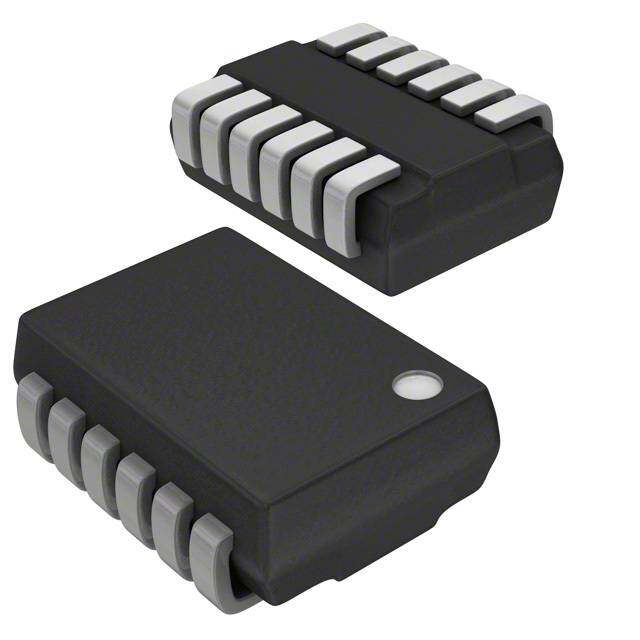
| 封装/外壳 | 20-TSSOP(0.173",4.40mm 宽) |
| 封装/箱体 | TSSOP-20 |
| 工作温度 | -40°C ~ 85°C |
| 工厂包装数量 | 74 |
| 应用说明 | 点击此处下载产品Datasheet点击此处下载产品Datasheet点击此处下载产品Datasheet点击此处下载产品Datasheet点击此处下载产品Datasheet点击此处下载产品Datasheet点击此处下载产品Datasheet点击此处下载产品Datasheet点击此处下载产品Datasheet点击此处下载产品Datasheet点击此处下载产品Datasheet点击此处下载产品Datasheet |
| 接口 | SPI |
| 日期格式 | YY-MM-DD-dd |
| 时间格式 | HH:MM:SS(12/24 小时) |
| 最大工作温度 | + 85 C |
| 最小工作温度 | - 40 C |
| 标准包装 | 1 |
| 特性 | 警报器,闰年,NVRAM,方波输出,涓流充电器 |
| 电压-电源 | 3 V ~ 5.5 V |
| 电压-电源,电池 | 1.3 V ~ 5.5 V |
| 电流-计时(最大) | 120µA ~ 160µA @ 3.63V ~ 5.5V |
| 电源电压-最大 | 5.5 V |
| 电源电压-最小 | 3 V |
| 类型 | 时钟/日历 |
| 系列 | DS1344E |
| 零件号别名 | 90-1344E+033 DS1344E |

.jpg)


PDF Datasheet 数据手册内容提取
DS1343/DS1344 Low-Current SPI/3-Wire RTCs General Description Features The DS1343/DS1344 low-current real-time clocks (RTCs) S Low Timekeeping Current of 250nA (typ) are timekeeping devices that provide an extremely low S Compatible with Crystal ESR Up to 100kI standby current, permitting longer life from a backup S Versions Available to Support Either 6pF or supply source. The devices also support high-ESR 12.5pF Crystals crystals, broadening the pool of usable crystals for the devices. The clock/calendar provides seconds, minutes, S RTC Counts Seconds, Minutes, Hours, Day, Date, hours, day, date, month, and year information. The date Month, and Year with Leap Year Compensation at the end of the month is automatically adjusted for Valid Through 2099 months with fewer than 31 days, including corrections S Power-Fail and Switch Circuitry for leap year. The clock operates in either 24-hour or S Three Operating Voltages 12-hour format with an AM/PM indicator. 1.8V ±5% Address and data are transferred serially through an 3.0V±10% SPI or 3-wire interface. Two programmable time-of-day 3.3V ±10% alarms are provided. Each alarm can generate an inter- S Trickle-Charge Capability rupt on a combination of seconds, minutes, hours, and day. Don’t-care states can be inserted into one or more S Maintain Time Down to 1.15V (typ) fields if it is desired for them to be ignored for the alarm S Support Motorola SPI Modes 1 and 3, or Standard condition. The time-of-day alarms can be programmed 3-Wire Interface to assert two different interrupt outputs, or they can be S Burst Mode for Reading/Writing Successive combined to assert one common interrupt output. Both Addresses in Clock/RAM interrupt outputs operate when the device is powered by either VCC or VBAT. S 96-Byte Battery-Backed NV RAM for Data Storage The devices are available in a lead-free/RoHS-compliant, S Two Time-of-Day Alarms with Two Interrupt 20-pin TSSOP or 14-pin TDFN package, and support a Outputs -40°C to +85°C extended industrial temperature range. S Industrial Temperature Range S 20-Pin TSSOP or 14-Pin TDFN Package Applications S Underwriters Laboratories (UL) Recognized Medical Handheld Devices Typical Operating Circuit Telematics Embedded Timestamping VCC RPU VCC INT INT0 X1 RST PF μP INT1 DS1343 Ordering Information appears at end of data sheet. 3-WIRE CE DS1344 X2 SCLK PORT SDI SDO VBAT SERMODE GND NOTE: SHOWN IN 3-WIRE I/O CONFIGURATION. For pricing, delivery, and ordering information, please contact Maxim Direct at 1-888-629-4642, or visit Maxim Integrated’s website at www.maximintegrated.com. 19-5801; Rev 2; 10/14
DS1343/DS1344 Low-Current SPI/3-Wire RTCs ABSOLUTE MAXIMUM RATINGS Voltage Range on VCC or VBAT Junction Temperature Maximum .....................................+150NC Relative to Ground ............................................-0.3V to +6.0V Storage Temperature Range ............................-55NC to +125NC Voltage Range on Any Nonpower Pin Lead Temperature (soldering, 10s) ................................+260NC Relative to Ground ................................-0.3V to (VCC + 0.3V) Soldering Temperature (reflow) ......................................+260NC Operating Temperature Range ..........................-40NC to +85NC Stresses beyond those listed under “Absolute Maximum Ratings” may cause permanent damage to the device. These are stress ratings only, and functional operation of the device at these or any other conditions beyond those indicated in the operational sections of the specifications is not implied. Exposure to absolute maximum rating conditions for extended periods may affect device reliability. PACKAGE THERMAL CHARACTERISTICS (Note 1) TSSOP TDFN Junction-to-Ambient Thermal Resistance (BJA) ..........91NC/W Junction-to-Ambient Thermal Resistance (BJA) ..........54NC/W Junction-to-Case Thermal Resistance (BJC) ...............20NC/W Junction-to-Case Thermal Resistance (BJC) .................8NC/W Note 1: P ackage thermal resistances were obtained using the method described in JEDEC specification JESD51-7, using a four-layer board. For detailed information on package thermal considerations, refer to www.maximintegrated.com/thermal-tutorial. RECOMMENDED OPERATING CONDITIONS (TA = -40°C to +85°C, unless otherwise noted.) (Note 2) PARAMETER SYMBOL CONDITIONS MIN TYP MAX UNITS DS134_-18 1.71 1.8 5.5 Operating Voltage Range VCC DS134_-3 2.7 3.0 5.5 V DS134_-33 3.0 3.3 5.5 Minimum Timekeeping Voltage VBATTMIN TA = +25NC 1.15 1.3 V Backup Voltage VBAT 1.3 5.5 V 0.7 x VCC + Logic 1 Input VIH V VCC 0.3 0.3 x Logic 0 Input VIL -0.3 V VCC DC ELECTRICAL CHARACTERISTICS (VCC = VCC(MIN) to +5.5V, VBAT = +1.3V to +5.5V, TA = -40°C to +85°C, unless otherwise noted.) (Notes 2, 3) PARAMETER SYMBOL CONDITIONS MIN TYP MAX UNITS Power-Supply Active Current ICCA -3 or -33: fSCLK = 4MHz (Note 4) 400 FA VCC = 3.63V 120 -33 VCC = VCC(MAX) 160 Power-Supply Standby Current VCC = 3.3V 130 ICCS -3 FA (Note 5) VCC = VCC(MAX) 175 VCC = 1.89V 120 -18 VCC = VCC(MAX) 200 Backup Leakage Current IBATLKG VCC > VPF -100 +25 +100 nA Backup Current (Oscillator Off) IBAT TA = +25NC, VCC = 0V, EOSC = 1 100 nA VBAT = 3V 250 DS1343 Backup Current VBAT = VBAT(MAX) 500 IBAT1 nA (Note 6) VBAT = 3V 350 DS1344 VBAT = VBAT(MAX) 600 2 Maxim Integrated
DS1343/DS1344 Low-Current SPI/3-Wire RTCs DC ELECTRICAL CHARACTERISTICS (continued) (VCC = VCC(MIN) to +5.5V, VBAT = +1.3V to +5.5V, TA = -40°C to +85°C, unless otherwise noted.) (Notes 2, 3) PARAMETER SYMBOL CONDITIONS MIN TYP MAX UNITS VBAT = 3V 300 DS1343 Backup Current VBAT = VBAT(MAX) 600 IBAT2 nA (Note 7) VBAT = 3V 400 DS1344 VBAT = VBAT(MAX) 700 Input Leakage (CE, SERMODE, II VIN = 0V to VCC -0.1 +0.1 FA SCLK, SDI) Output Leakage IO CE = VIL, no alarms -0.1 +0.1 FA (INT0, INT1, PF, SDO) -3 or -33: VOH = 2.4V -1 Output Logic 1 (PF, SDO) IOH mA -18: VOH = 1V -0.5 -3 or -33: VOL = 0.4V 3.0 Output Logic 0 -18: VOL = 0.4V 2.0 IOL mA (INT0, INT1, PF, SDO) VBAT R 1.3V R VCC + 0.2V, VOL = 0.2V 0.25 (Note 8) -18 1.51 1.6 1.71 Power-Fail Trip Point VPF -3 2.45 2.6 2.70 V -33 2.70 2.88 3.0 VBAT > VPF VPF Switchover Voltage VSW V VBAT < VPF VBAT > VCC R1 1 Trickle-Charger Resistors R2 2 kI R3 4 AC ELECTRICAL CHARACTERISTICS (VCC = VCC(MIN) to VCC(MAX), TA = -40°C to +85°C, unless otherwise noted.) (Notes 2, 3) PARAMETER SYMBOL CONDITIONS MIN TYP MAX UNITS -18 DC 1 SCLK Frequency fSCLK MHz -3 or -33 DC 4 Data to SCLK Setup tDC 30 ns SCLK to Data Hold tCDH 30 ns -18 240 SCLK to Data Delay tCDD ns -3 or -33 80 -18 400 SCLK Low Time tCL ns -3 or -33 110 -18 400 SCLK High Time tCH ns -3 or -33 110 Maxim Integrated 3
DS1343/DS1344 Low-Current SPI/3-Wire RTCs AC ELECTRICAL CHARACTERISTICS (continued) (VCC = VCC(MIN) to VCC(MAX), TA = -40°C to +85°C, unless otherwise noted.) (Notes 2, 3) SCLK Rise and Fall tR, tF 200 ns CE to SCLK Setup tCC 400 ns SCLK to CE Hold tCCH 100 ns -18 500 CE Inactive Time tCWH ns -3 or -33 400 CE to Output High-Z tCDZ 80 ns Oscillator Stop Flag (OSF) Delay tOSF (Note 9) 25 100 ms POWER-UP/DOWN CHARACTERISTICS (TA = -40°C to +85°C, unless otherwise noted.) PARAMETER SYMBOL CONDITIONS MIN TYP MAX UNITS Recovery at Power-Up tREC 20 40 ms VCC Fall Time (VPF to 0V) tVCCF 150 Fs VCC Rise Time (0V to VPF) tVCCR 0 Fs CAPACITANCE (TA = +25°C, unless otherwise noted.) PARAMETER SYMBOL CONDITIONS MIN TYP MAX UNITS Input Capacitance CI (Note 10) 10 pF Output Capacitance CO (Note 10) 15 pF CRYSTAL PARAMETERS PARAMETER SYMBOL CONDITIONS MIN TYP MAX UNITS Nominal Frequency fO 32.768 kHz Series Resistance ESR 100 kI DS1343 6 Load Capacitance CL pF DS1344 12.5 Note 2: Voltage referenced to ground. Note 3: Limits at TA = -40°C are guaranteed by design and not production tested. Note 4: CE = VCC, VSCLK = VCC to GND, IOUT = 0mA, trickle charger disabled. Note 5: CE = GND, IOUT = 0mA, EOSC = EGFIL = DOSF = 0, trickle charger disabled. Note 6: VCC = 0V, EGFIL = 0, DOSF = 1. Note 7: VCC = 0V, EGFIL = 1, DOSF = 0. Note 8: Applies to INT0 and INT1. Note 9: The parameter tOSF is the period of time the oscillator must be stopped for the OSF flag to be set. Note 10: Guaranteed by design; not 100% production tested. 4 Maxim Integrated
DS1343/DS1344 Low-Current SPI/3-Wire RTCs SPI Write Timing tCWH CE tCC tF tCCH tCL tCH tR SCLK* tCDH tDC tCDH SDI R/W = 1 A6 A0 D7 D0 WRITE ADDRESS BYTE WRITE DATA BYTE *SCLK CAN BE EITHER POLARITY. TIMING SHOWN FOR CPOL = 1. SERMODE = VCC. SPI Read Timing tCWH CE tCC tCL tCH SCLK* tCDH tDC tCDD tCDZ SDI R/W = 0 A6 A0 SDO D7 D0 WRITE ADDRESS BYTE READ DATA BYTE *SCLK CAN BE EITHER POLARITY. TIMING SHOWN FOR CPOL = 1. SERMODE = VCC. Maxim Integrated 5
DS1343/DS1344 Low-Current SPI/3-Wire RTCs 3-Wire Write Timing tCWH CE tCCH tCC tCL tR tF SCLK tCDH tCH tDC I/O* A0 A1 R/W = 1 D0 D7 WRITE ADDRESS BYTE WRITE DATA BYTE *I/O IS SDI AND SDO CONNECTED TOGETHER. SERMODE = GND. 3-Wire Read Timing tCWH CE tCC tCL tCDD tCDZ SCLK tCDH tCH tDC I/O* A0 A1 R/W = 0 D0 D7 WRITE ADDRESS BYTE READ DATA BYTE *I/O IS SDI AND SDO CONNECTED TOGETHER. SERMODE = GND. 6 Maxim Integrated
DS1343/DS1344 Low-Current SPI/3-Wire RTCs Typical Operating Characteristics (VCC = +3.3V, TA = +25°C, unless otherwise noted.) POWER-SUPPLY CURRENT POWER-SUPPLY CURRENT vs. POWER-SUPPLY VOLTAGE vs. POWER-SUPPLY VOLTAGE 600 140 500 TICOAEU =T= +=V2 I0H5m°CA DS1343/4 toc01 130 CIOEU T= =V I0LmA DS1343/4 toc02 NT (µA) 400 NT (µA) 112100 TA = +85°C RE fSCLK = 4MHz RE UR 300 UR 100 TA = +25°C C C Y Y PL PL 90 UP 200 UP S fSCLK = 1MHz S 80 100 TA = -40°C 70 0 60 3.0 3.5 4.0 4.5 5.0 5.5 3.0 3.5 4.0 4.5 5.0 5.5 SUPPLY VOLTAGE (V) SUPPLY VOLTAGE (V) DS1343 BATTERY CURRENT1 DS1343 BATTERY CURRENT2 vs. BATTERY VOLTAGE vs. BATTERY VOLTAGE 226800 EDIOGOUFSTI FL= ==0 m10A DS1343/4 toc03 332400 EDIOGOUFSTI FL= ==0 m01A DS1343/4 toc04 NT (nA) 240 TA = +85°C NT (nA) 238000 TA = +85°C RE 220 RE CUR CUR 260 TA = +25°C RY 200 TA = +25°C RY BATTE 180 TA = -40°C BATTE 222400 TA = -40°C 160 200 140 180 1.0 1.5 2.0 2.5 3.0 3.5 4.0 4.5 5.0 5.5 1.0 1.5 2.0 2.5 3.0 3.5 4.0 4.5 5.0 5.5 BATTERY VOLTAGE (V) BATTERY VOLTAGE (V) DS1344 BATTERY CURRENT1 DS1344 BATTERY CURRENT2 vs. BATTERY VOLTAGE vs. BATTERY VOLTAGE 380 440 334600 EGFIL = 0, DOSF = 1, IOUT = 0mA DS1343/4 toc05 EGFIL = 1, DOSF = 0, IOUT = 0mA DS1343/4 toc06 A) A) 390 NT (n 320 TA = +85°C NT (n TA = +85°C RRE 300 RRE TA = +25°C U U 340 C C Y 280 TA = +25°C Y R R E E TT 260 TT A A B 240 TA = -40°C B 290 TA = -40°C 220 200 240 1.0 1.5 2.0 2.5 3.0 3.5 4.0 4.5 5.0 5.5 1.0 1.5 2.0 2.5 3.0 3.5 4.0 4.5 5.0 5.5 BATTERY VOLTAGE (V) BATTERY VOLTAGE (V) Maxim Integrated 7
DS1343/DS1344 Low-Current SPI/3-Wire RTCs Pin Configurations TOP VIEW E D TOP VIEW O VBAT 1 + 20 VCC VCC SERM PF SDO SDI SCLK CE 14 13 12 11 10 9 8 N.C. 2 19 N.C. X1 3 18 PF N.C. 4 DS1343 17 N.C. DS1344 X2 5 16 SDO DS1343 DS1344 N.C. 6 15 SDI INT0 7 14 SCLK N.C. 8 13 N.C. + EP INT1 9 12 CE 1 2 3 4 5 6 7 GND 10 11 SERMODE TSSOP VBAT X1 X2 INT0 N.C. INT1 GND TDFN (3mm × 3mm) Pin Descriptions PIN NAME FUNCTION TSSOP TDFN-EP Battery Input for Standard +3V Lithium Cell or Other Energy Source. UL recognized 1 1 VBAT to ensure against reverse charging current when used in conjunction with a primary lithium battery. 2, 4, 6, 8, No Connection. N.C. pins can be connected to GND to reduce noise around the 5 N.C. 13, 17, 19 crystal inputs. Connections for Standard 32.768kHz Quartz Crystal (see the Crystal Characteristics 3 2 X1 table). The devices can also be driven by an external 32.768kHz oscillator. In this configuration, the X1 pin is connected to the external oscillator and the X2 pin is left 5 3 X2 unconnected. Active-Low Interrupt 0 Output. INT0 is an active-low output that can be used as an interrupt output to a processor. INT0 can be programmed to be asserted by only Alarm 0, or can be programmed to be asserted by either Alarm 0 or Alarm 1. 7 4 INT0 INT0 remains low as long as the status bit causing the interrupt is present and the corresponding interrupt enable bit is set. INT0 operates when the component is powered by VCC or VBAT. INT0 is an open-drain output and requires an external pullup resistor. Active-Low Interrupt 1 Output. INT1 is an active-low output that can be used either as an interrupt output to a processor or a 32kHz square-wave output. INT1 can be programmed to be asserted by Alarm 1 only. INT1 remains low as long as the status 9 6 INT1 bit causing the interrupt is present and the corresponding interrupt enable bit is set. INT1 operates when the component is powered by VCC or VBAT. INT1 is an open- drain output and requires an external pullup resistor. 8 Maxim Integrated
DS1343/DS1344 Low-Current SPI/3-Wire RTCs Pin Descriptions (continued) PIN NAME FUNCTION TSSOP TDFN-EP 10 7 GND Ground Serial-Interface Mode Input. When connected to GND, standard 3-wire 11 13 SERMODE communication is selected. When connected to VCC, SPI communication is selected. Chip Enable. The chip-enable signal must be asserted high during a read or a write 12 8 CE for either 3-wire or SPI communications. Serial-Clock Input. SCLK is used to synchronize data movement on the serial 14 9 SCLK interface for either 3-wire or SPI communications. Serial-Data Input. When SPI communication is selected, SDI is the serial-data input 15 10 SDI for the SPI bus. When 3-wire communication is selected, this pin must be connected to SDO (SDI and SDO function as a single I/O pin when connected together). Serial-Data Output. When SPI communication is selected, SDO is the serial-data output for the SPI bus. When 3-wire communication is selected, this pin must be 16 11 SDO connected to SDI (SDI and SDO function as a single I/O pin when connected together). Active-Low Power-Fail Output. The PF pin is used to indicate loss of the primary 18 12 PF power supply (VCC). When VCC is less than VPF, the PF pin is driven low. 20 14 VCC Power-Supply Input — — EP Exposed Pad (TDFN Only). Connect to GND or leave unconnected. Functional Diagram 32.768kHz X1 X2 VCC OSCILLATOR AND POWER CONTROL 1Hz PF COUNTDOWN CHAIN AND INT0 VBAT TRICKLE CHARGER GND CLOCK, CALENDAR, AND N ALARM REGISTERS ON_VCC DS1343 CONTROL DS1344 REGISTERS INT1 CE N SCLK INPUT SERIAL SDI SHIFT USER RAM INTERFACE SDO REGISTER SERMODE Maxim Integrated 9
DS1343/DS1344 Low-Current SPI/3-Wire RTCs Detailed Description when VCC falls below VPF, the internal clock registers are blocked from any access, and the device power is The DS1343/DS1344 low-current real-time clocks (RTCs) switched from VCC to VBAT. are timekeeping devices that consume an extremely low timekeeping current and also support high-ESR crystals, If VPF is less than the voltage on the backup supply, the broadening the pool of usable crystals for the device. device power is switched from VCC to the backup sup- ply when VCC drops below VPF. If VPF is greater than the The devices provide a full binary-coded decimal (BCD) backup supply, the device power is switched from VCC clock calendar that is accessed by a simple serial inter- to the backup supply when VCC drops below the backup face. The clock/calendar provides seconds, minutes, supply. The registers are maintained from the backup hours, day, date, month, and year information. The date supply source until VCC is returned to nominal levels. at the end of the month is automatically adjusted for The Functional Diagram illustrates the main elements. months with fewer than 31 days, including corrections for leap year through 2099. The clock operates in either Freshness Seal Mode a 24-hour or 12-hour format with an AM/PM indicator. In When a battery is first attached to the device, the device addition, 96 bytes of NV RAM are provided for data stor- does not immediately provide battery-backup power to age. The devices maintain the time and date, provided the RTC or internal circuitry. After VCC exceeds VPF, that the oscillator is enabled, as long as at least one sup- the devices leave the freshness seal mode and provide ply is at a valid level. battery-backup power whenever VCC subsequently falls Both devices provide two programmable time-of-day below VBAT. This mode allows attachment of the battery during product manufacturing, but no battery capacity is alarms. Each alarm can generate an interrupt on a pro- consumed until after the system has been activated for grammable combination of seconds, minutes, hours, and the first time. As a result, minimum battery energy is used day. Don’t-care states can be inserted into one or more during storage and shipping. fields if it is desired for them to be ignored for the alarm condition. The time-of day alarms can be programmed Oscillator Circuit to assert two different interrupt outputs or to assert one The devices use an external 32.768kHz crystal. The common interrupt output. Both interrupt outputs operate oscillator circuit does not require any external resistors or when the device is powered by VCC or VBAT. capacitors to operate. The DS1343 includes integrated The devices support a direct interface to SPI serial-data capacitive loading for a 6pF CL crystal, and the DS1344 ports or standard 3-wire interface. A straight-forward includes integrated capacitive loading for a 12.5pF CL address and data format is implemented in which data crystal. See the Crystal Parameters table for the external transfers can occur one byte at a time or in multiple-byte crystal parameters. The Functional Diagram shows a burst mode. simplified schematic of the oscillator circuit. The startup time is usually less than one second when using a crystal The devices have a built-in temperature-compensated with the specified characteristics. power-sense circuit that detects power failures and automatically switches to the backup supply. The VBAT Clock Accuracy pin can be configured to provide trickle charging of a When running from the internal oscillator, the accuracy of rechargeable voltage source, with selectable charging the clock is dependent upon the accuracy of the crystal resistance and diode-voltage drops. and the accuracy of the match between the capacitive load of the oscillator circuit and the capacitive load for I/O and Power-Switching Operation which the crystal was trimmed. Additional error is added The devices operate as slave devices on a 3-wire or SPI by crystal frequency drift caused by temperature shifts. serial bus. Access is obtained by selecting the part by External circuit noise coupled into the oscillator circuit the CE pin and clocking data into/out of the part using can result in the clock running fast. Figure 1 shows a the SCLK and SDI/SDO pins. Multiple byte transfers typical PCB layout for isolation of the crystal and oscil- are supported within one CE high period; see the Serial lator from noise. Refer to Application Note 58: Crystal Peripheral Interface (SPI) section for more information. Considerations with Dallas Real-Time Clocks for detailed The devices are fully accessible and data can be writ- information. ten and read when VCC is greater than VPF. However, 10 Maxim Integrated
DS1343/DS1344 Low-Current SPI/3-Wire RTCs LOCAL GROUND PLANE (LAYER 2) X1 CRYSTAL X2 NOTE: AVOID ROUTING SIGNAL LINES IN THE CROSSHATCHED AREA (UPPER LEFT QUADRANT) OF THE PACKAGE UNLESS THERE IS GND A GROUND PLANE BETWEEN THE SIGNAL LINE AND THE DEVICE PACKAGE. Figure 1. Layout Example Register Map 7 of Month) is toggled when the Years register rolls over from 99 to 00. On a power-on reset (POR), the time and Table 1 shows the devices’ register map. During a mul- date are set to 00:00:00 01/01/00 (hh:mm:ss DD/MM/YY), tibyte RTC access, if the address pointer reaches the and the Day register is set to 01. end of the register space (1Fh), it wraps around to loca- tion 00h. During a multibyte RAM access, if the address Alarms (07h–0Eh) pointer reaches the end of the register space (7Fh), it The devices contains two time-of-day/date alarms. Alarm wraps around to location 20h. On either the rising edge 0 can be set by writing to registers 07h–0Ah. Alarm 1 can of CE or an RTC address pointer wrap around, the cur- be set by writing to registers 0Bh–0Eh. The alarms can rent time is transferred to a secondary set of registers. be programmed to activate the INT0 or INT1 outputs on The time information is read from these secondary regis- an alarm match condition (see Table 2). Bit 7 of each ters, while the clock continues to run. This eliminates the of the time of day/date alarm registers are mask bits. need to reread the registers in case the main registers When all the mask bits for each alarm are 0, an alarm update during a read. only occurs when the values in the timekeeping registers 00h–06h match the values stored in the alarm registers. Clock and Calendar (00h–06h) The alarms can also be programmed to repeat every The time and calendar information is obtained by reading second, minute, hour, or day. Configurations not listed the appropriate register bytes. Table 1 shows the RTC in the table result in illogical operation. POR values are registers. The time and calendar are set or initialized by undefined. writing the appropriate register bytes. The contents of When the RTC register values match alarm register the time and calendar registers are in the BCD format. settings, the corresponding alarm flag bit (IRQF0 or The Day register increments at midnight and rolls over IRQF1) is set to 1 in the Status register. If the corre- from 7 to 1. Values that correspond to the day-of-week sponding alarm interrupt enable bit (A0IE or A1IE) is are user defined, but must be sequential (i.e., if 1 equals also set to 1 in the Control register, the alarm condition Sunday, then 2 equals Monday, and so on). Illogical time activates the output(s) defined by the INTCN bit. Upon and date entries result in undefined operation. an active alarm, clearing the associated IRQF[1:0] bit The devices can be run in either 12-hour or 24-hour deasserts the selected interrupt output while leaving mode. Bit 6 of the Hours register is defined as the 12- or the alarm enabled for the next occurrence of a match. 24-hour mode-select bit. When high, the 12-hour mode Alternatively, clearing the A_IE bit deasserts the output is selected. In the 12-hour mode, bit 5 is the AM/PM bit, and inhibits further output activations. with a content of 1 being PM. In the 24-hour mode, bit 5 The alarm flags are always active, fully independent of is the 20-hour field. Changing the 12/24 mode-select bit the A_IE bit states. All alarm registers should be written requires that the Hours data subsequently be reentered, to logic zero to disable the alarm matching. including the Alarm register (if used). The Century bit (bit Maxim Integrated 11
DS1343/DS1344 Low-Current SPI/3-Wire RTCs Table 1. Register Map BIT 7 BIT 0 ADDRESS BIT 6 BIT 5 BIT 4 BIT 3 BIT 2 BIT 1 FUNCTION RANGE MSB LSB 00h 0 10 Seconds Seconds Seconds 00–59 01h 0 10 Minutes Minutes Minutes 00–59 AM/PM 1–12 + 10 02h 0 12/24 20 Hour Hours AM/PM Hours Hours 00–23 03h 0 0 0 0 0 Day Day 1–7 04h 0 0 10 Date Date Date 01–31 10 Month/ 01–12 + 05h Century 0 0 Month Month Century Century 06h 10 Year Year Year 00–99 Alarm 0 07h A0M1 10 Seconds Seconds 00–59 Seconds Alarm 0 08h A0M2 10 Minutes Minutes 00–59 Minutes AM/PM 1–12 + 10 09h A0M3 12/24 20 Hour Alarm 0 Hours AM/PM Hours Hours 00–23 0Ah A0M4 0 0 0 Day Alarm 0 Day 1–7 Alarm 1 0Bh A1M1 10 Seconds Seconds 00–59 Seconds Alarm 1 0Ch A1M2 10 Minutes Minutes 00–59 Minutes AM/PM 1–12 + 10 0Dh A1M3 12/24 20 Hour Alarm 1 Hours AM/PM Hours Hours 00–23 0Eh A1M4 0 0 0 Day Alarm 1 Day 1–7 0Fh EOSC X DOSF EGFIL SQW INTCN A1IE A0IE Control — 10h OSF 0 0 0 0 0 IRQF1 IRQF0 Status — Trickle 11h TCS3 TCS2 TCS1 TCS0 DS1 DS0 RS1 RS0 — Charger 12h–1Fh Reserved Reserved — 20h–7Fh User RAM User RAM 00h–FFh Note: Bits listed as 0 always read back as 0 and cannot be written to 1. Table 2. Alarm Mask Bits ALARM REGISTER MASK BITS (BIT 7) ALARM RATE A_M4 A_M3 A_M2 A_M1 1 1 1 1 Alarm once a second 1 1 1 0 Alarm when seconds match 1 1 0 0 Alarm when minutes and seconds match 1 0 0 0 Alarm when hours, minutes, and seconds match 0 0 0 0 Alarm when day, hours, minutes, and seconds match 12 Maxim Integrated
DS1343/DS1344 Low-Current SPI/3-Wire RTCs Control Register (0Fh) BIT 7 BIT 6 BIT 5 BIT 4 BIT 3 BIT 2 BIT 1 BIT 0 EOSC X DOSF EGFIL SQW INTCN A1IE A0IE 1 0 0 0 0 0 0 0 EOSC: Enable oscillator. During battery backup, when EOSC is set to 0, the oscillator is enabled during back- BIT 7 up operation. When set to 1, the oscillator is stopped when the device is powered by the backup supply. This bit is set to logic 1 on the initial application of power. BIT 6 Not used. DOSF: Disable oscillator stop flag. When the DOSF bit is set to 1, sensing of the oscillator conditions that BIT 5 would set the OSF bit are disabled. OSF remains at 0 regardless of what happens to the oscillator. This bit is cleared (0) on the initial application of power. EGFIL: Enable glitch filter. When the EGFIL bit is 1, the 5Fs glitch filter at the output of crystal oscillator is BIT 4 enabled. The glitch filter is disabled when this bit is 0. This bit is cleared (0) on the initial application of power. SQW: Enable square wave. When the SQW bit is set to 1, a 32kHz square wave is output on the INT1 output. BIT 3 This bit is cleared (0) on the initial application of power. INTCN: Interrupt control. This bit controls the relationship between the two time-of-day alarms and the two interrupt output pins. When the INTCN bit is 1, a match between the timekeeping registers and the Alarm 0 registers activates the INT0 output (provided A0IE = 1), and a match between the timekeeping registers BIT 2 and the Alarm 1 registers activates the INT1 output (provided A1IE = 1). When the INTCN bit is 0, a match between the timekeeping registers and either the Alarm 0 registers or Alarm 1 registers activates the INT0 out- put (provided A0IE = A1IE = 1). The INT1 output has no function when INTCN = 0. The INTCN bit is cleared (0) on the initial application of power. A1IE: Alarm 1 interrupt enable. When A1IE is set to 0, the Alarm 1 interrupt function is disabled. When A1IE is 1, the Alarm 1 interrupt function is enabled and is routed to either INT0 (if INTCN = 0) or INT1 (if INTCN BIT 1 = 1). Regardless of the state of A1IE, a match between the timekeeping registers and the Alarm 1 registers (0Bh–0Eh) sets the interrupt request 1 flag bit (IRQF1). The A1IE bit is cleared (0) when power is first applied. A0IE: Alarm 0 interrupt enable. When A0IE is set to 0, the Alarm 0 interrupt function is disabled. When A0IE is 1, the Alarm 0 interrupt function is enabled and is routed to INT0. Regardless of the state of A0IE, a match BIT 0 between the timekeeping registers and the Alarm 0 registers (07h–0Ah) sets the interrupt register 0 flag bit (IRQF0). The A0IE bit is cleared (0) when power is first applied. Maxim Integrated 13
DS1343/DS1344 Low-Current SPI/3-Wire RTCs Status Register (10h) BIT 7 BIT 6 BIT 5 BIT 4 BIT 3 BIT 2 BIT 1 BIT 0 OSF 0 0 0 0 0 IRQF1 IRQF0 1 0 0 0 0 0 0 0 OSF: Oscillator stop flag. If the OSF bit is 1, the oscillator either has stopped or was stopped for some period and could be used to judge the validity of the clock and calendar data. This bit is edge triggered and is set to 1 when the internal circuitry senses the oscillator has transitioned from a normal run state to a stop condition. This bit remains at logic 1 until written to logic 0. Attempting to write OSF to 1 leaves the value unchanged. BIT 7 The following are examples of conditions that can cause the OSF bit to be set: 1) The first time power is applied. 2) The voltage present on VCC is insufficient to support oscillation. 3) The EOSC bit is a logic one during battery backup. 4) External influences on the crystal (i.e., noise, leakage, etc.). IRQF1: Interrupt request 1 flag. A logic 1 in the IRQF1 bit indicates that the time matched the Alarm 1 reg- isters. This flag can be used to generate an interrupt on either INT0 or INT1 depending on the status of the INTCN bit in the Control register. If the INTCN bit is 0 and IRQF1 is 1 (and the A1IE bit is also 1), INT0 goes BIT 1 low. If the INTCN bit is 1 and IRQF1 is 1 (and the A1IE bit is also 1), INT1 goes low. IRQF1 is cleared when the address pointer is set to any of the Alarm 1 registers during an I/O transaction. The IRQF1 bit can also be cleared by writing it to 0. This bit can only be written to 0. Attempting to write the IRQF1 bit to 1 leaves the value unchanged. IRQF0: Interrupt request 0 flag. A logic 1 in the IRQF0 bit indicates that the time matched the Alarm 0 regis- ters. If the A0IE bit is also 1, INT0 goes low. IRQF0 is cleared when the address pointer is set to any of the BIT 0 Alarm 0 registers during an I/O transaction. The IRQF0 bit can also be cleared by writing it to 0. This bit can only be written to 0. Attempting to write the IRQF0 bit to 1 leaves the value unchanged. Trickle Charger Register (11h) BIT 7 BIT 6 BIT 5 BIT 4 BIT 3 BIT 2 BIT 1 BIT 0 TCS3 TCS2 TCS1 TCS0 DS1 DS0 RS1 RS0 0 0 0 0 0 0 0 0 Register 11h controls the devices’ trickle-charge char- (DS[1:0]) bits (bits 3:2) select whether or not a diode is acteristics. The simplified schematic of Figure 2 shows connected between VCC and VBAT. The resistor-select the basic components of the trickle charger. The trickle- (RS[1:0]) bits (bits 1:0) select the resistor that is con- charge select (TCS[3:0]) bits (bits 7:4) control the nected between VCC and VBAT. The RS and DS bits selection of the trickle charger. To prevent accidental select the resistor and diodes, as shown in Table 3. The enabling, only a pattern of 1010 enables the trickle user determines diode and resistor selection according charger; all other patterns disable the trickle charger. to the maximum current desired for secondary battery or On the initial application of power, the devices power super cap charging. The maximum charging current can up with the trickle charger disabled. The diode-select be calculated using the equation that follows. 14 Maxim Integrated
DS1343/DS1344 Low-Current SPI/3-Wire RTCs R1 1kΩ VCC R2 VBAT 2kΩ R3 4kΩ 1 0F 18 SELECT 1 OF 2 1 OF 3 NOTE: ONLY 1010 CODE ENABLES CHARGER SELECT SELECT TCS = TRICKLE-CHARGER SELECT DS = DIODE SELECT RS = RESISTOR SELECT TRICKLE CHARGER TCS TCS TCS TCS DS DS RS RS REGISTER BIT 7 BIT 6 BIT 5 BIT 4 BIT 3 BIT 2 BIT 1 BIT 0 Figure 2. Trickle Charger Block Diagram Table 3. Trickle-Charger Resistor and Diode Select TCS3 TCS2 TCS1 TCS0 DS1 DS0 RS1 RS0 FUNCTION X X X X X X 0 0 Disabled X X X X 0 0 X X Disabled X X X X 1 1 X X Disabled 1 0 1 0 0 1 0 1 No diode, 1kI 1 0 1 0 0 1 1 0 No diode, 2kI 1 0 1 0 0 1 1 1 No diode, 4kI 1 0 1 0 1 0 0 1 One diode, 1kI 1 0 1 0 1 0 1 0 One diode, 2kI 1 0 1 0 1 0 1 1 One diode, 4kI 0 0 0 0 0 0 0 0 Initial power-on state—disabled X = Don’t care. Assume, for the purposes of the example, that a system Serial Port Operation power supply of 5V is applied to VCC and a super cap is The devices offer the flexibility to choose between two connected to VBAT. Also assume that the trickle charger serial-interface modes. The component can commu- has been enabled with one diode and resistor R1. The nicate with the SPI interface or with a standard 3-wire maximum current IMAX would be calculated as follows: interface. The interface method used is determined by IMAX = (5.0V - diode drop)/R1 ≈ (5.0V - 0.6V)/2kΩ ≈ SERMODE. When SERMODE is connected to VCC, SPI 2.2mA communication is selected. When SERMODE is con- As the super cap charges, the voltage drop between nected to ground, standard 3-wire communication is VCC and VBAT decreases, and therefore, the charge selected. current decreases. Maxim Integrated 15
DS1343/DS1344 Low-Current SPI/3-Wire RTCs Serial Peripheral Interface (SPI) Address and Data Bytes Address and data bytes are shifted MSB first into the The serial peripheral interface (SPI) is a synchronous serial-data input (SDI) and out of the serial-data output bus for address and data transfer, and is used when (SDO). Any transfer requires the address of the byte to interfacing with the SPI bus on specific Motorola micro- specify a write or read to either a RTC or RAM location, controllers, such as the 68HC05C4 and the 68HC11A8. followed by one or more bytes of data. Data is trans- The SPI mode of serial communication is selected by ferred out of the SDO for a read operation and into the connecting SERMODE to VCC. Four pins are used for the SDI for a write operation (Figure 4 and Figure 5). SPI. The four pins are SDO (serial-data out), SDI (serial- data in), CE (chip enable), and SCLK (serial clock). The The address byte is always the first byte entered after CE IC is the slave device in an SPI application, with the is driven high. The most significant bit (R/W) of this byte microcontroller being the master. determines if a read or write takes place. If R/W is 0, one or more read cycles occur. If R/W is 1, one or more write SDI and SDO are the serial-data input and output pins, cycles occur. respectively, for the device. The CE input is used to initiate and terminate a data transfer. SCLK is used to Data transfers can occur 1 byte at a time or in multiple- synchronize data movement between the master (micro- byte burst mode. After CE is driven high an address is controller) and the slave (IC) devices. written to the device. After the address, one or more data bytes can be written or read. For a single-byte transfer, The input clock (SCLK), which is generated by the micro- 1 byte is read or written and then CE is driven low. For controller, is active only during address and data transfer a multiple-byte transfer, however, multiple bytes can to any device on the SPI bus. The inactive clock polarity be read or written to the device after the address has is programmable in some microcontrollers. The device been written. Each read or write cycle causes the RTC determines the clock polarity by sampling SCLK when register or RAM address to automatically increment. CE becomes active. Therefore, either SCLK polarity can Incrementing continues until the device is disabled. be accommodated. Input data (SDI) is latched on the When the RTC address space is selected, the address internal strobe edge and output data (SDO) is shifted out wraps to 00h after incrementing from 1Fh. When the on the shift edge (Figure 3). There is one clock for each RAM address space is selected, the address wraps to bit transferred. Address and data bits are transferred in 20h after incrementing from 7Fh. groups of eight, MSB first. CE CPOL = 1 SCLK SHIFT DATA OUT (READ) DATA LATCH (WRITE) CPOL = 0 SCLK SHIFT DATA OUT (READ) DATA LATCH (WRITE) NOTE 1: CPHA BIT POLARITY (IF APPLICABLE) MAY NEED TO BE SET ACCORDINGLY. NOTE 2: CPOL IS A BIT THAT IS SET IN THE MICROCONTROLLER’S CONTROL REGISTER. NOTE 3: SDO REMAINS AT HIGH-Z UNTIL 8 BITS OF DATA ARE READY TO BE SHIFTED OUT DURING A READ. Figure 3. Serial Clock as a Function of Microcontroller Clock Polarity (CPOL) 16 Maxim Integrated
DS1343/DS1344 Low-Current SPI/3-Wire RTCs CE SCLK* SDI 1 A6 A5 A4 A3 A2 A1 A0 D7 D6 D5 D4 D3 D2 D1 D0 R/W HIGH-Z SDO *SCLK CAN BE EITHER POLARITY. SERMODE = VCC. Figure 4. SPI Single-Byte Write CE SCLK* SDI 0 A6 A5 A4 A3 A2 A1 A0 R/W HIGH-Z SDO D7 D6 D5 D4 D3 D2 D1 D0 *SCLK CAN BE EITHER POLARITY. SERMODE = VCC. Figure 5. SPI Single-Byte Read CE SCLK ADDRESS DATA DATA DATA WRITE SDI BYTE BYTE 0 BYTE 1 BYTE N ADDRESS SDI BYTE READ DATA DATA DATA SDO BYTE 0 BYTE 1 BYTE N Figure 6. SPI Multibyte Burst Transfer Maxim Integrated 17
DS1343/DS1344 Low-Current SPI/3-Wire RTCs Reading and Writing in Burst Mode Applications Information Burst mode is similar to a single-byte read or write, except that CE is kept high and additional SCLK cycles Power-Supply Decoupling are sent until the end of the burst. The clock registers To achieve the best results when using the devices, and the user RAM can be read or written in burst mode. decouple the VCC power supply with a 0.01µF and/or The address pointer wraps around to 00h after reaching 0.1µF capacitor. Use a high-quality, ceramic, surface- 1Fh (RTC), and the address pointer wraps around to 20h mount capacitor if possible. Surface-mount components after reaching 7Fh (RAM). See Figure 6. minimize lead inductance, which improves performance, and ceramic capacitors tend to have adequate high- 3-Wire Interface frequency response for decoupling applications. The 3-wire interface mode operates similarly to the SPI Using Open-Drain Outputs mode. However, in 3-wire mode there is one I/O instead The INT0 and INT1 outputs are open drain and therefore of separate data-in and data-out signals. The 3-wire require external pullup resistors to realize a logic-high interface consists of the I/O (SDI and SDO pins con- output level. nected together), CE, and SCLK pins. In 3-wire mode, Battery Charge Protection each byte is shifted in LSB first, unlike SPI mode, where The devices contain Maxim’s redundant battery-charge each byte is shifted in MSB first. protection circuit to prevent any charging of an external As is the case with the SPI mode, an address byte is battery. The DS1343 and DS1344 are recognized by written to the device followed by a single data byte or Underwriters Laboratories (UL) under file E141114. multiple data bytes. Figure 7 illustrates a write cycle, and Figure 8 illustrates a read cycle. In 3-wire mode, data is input on the rising edge of SCLK and output on the falling edge of SCLK. CE SCLK HIGH-Z I/O* A0 A1 A2 A3 A4 A5 A6 1 D0 D1 D2 D3 D4 D5 D6 D7 *I/O IS SDI AND SDO CONNECTED TOGETHER. R/W SERMODE = GND. Figure 7. 3-Wire Single-Byte Write CE SCLK HIGH-Z I/O* A0 A1 A2 A3 A4 A5 A6 0 D0 D1 D2 D3 D4 D5 D6 D7 *I/O IS SDI AND SDO CONNECTED TOGETHER. R/W SERMODE = GND Figure 8. 3-Wire Single-Byte Read 18 Maxim Integrated
DS1343/DS1344 Low-Current SPI/3-Wire RTCs Ordering Information TYP OPERATING OSC CL PART TEMP RANGE PIN-PACKAGE VOLTAGE (V) (pF) DS1343E-18+ -40NC to +85NC 1.8 6 20 TSSOP DS1343E-3+ -40NC to +85NC 3.0 6 20 TSSOP DS1343E-33+ -40NC to +85NC 3.3 6 20 TSSOP DS1343D-18+ -40NC to +85NC 1.8 6 14 TDFN-EP* DS1343D-3+ -40NC to +85NC 3.0 6 14 TDFN-EP* DS1343D-33+ -40NC to +85NC 3.3 6 14 TDFN-EP* DS1344E-18+ -40NC to +85NC 1.8 12.5 20 TSSOP DS1344E-3+ -40NC to +85NC 3.0 12.5 20 TSSOP DS1344E-33+ -40NC to +85NC 3.3 12.5 20 TSSOP DS1344D-18+ -40NC to +85NC 1.8 12.5 14 TDFN-EP* DS1344D-3+ -40NC to +85NC 3.0 12.5 14 TDFN-EP* DS1344D-33+ -40NC to +85NC 3.3 12.5 14 TDFN-EP* +Denotes a lead(Pb)-free/RoHS-compliant package. *EP = Exposed pad. Chip Information Package Information SUBSTRATE CONNECTED TO GROUND For the latest package outline information and land patterns (footprints), go to www.maximintegrated.com/packages. Note that a “+”, “#”, or “-” in the package code indicates RoHS status only. Package drawings may show a different suffix character, but the drawing pertains to the package regardless of RoHS status. PACKAGE PACKAGE OUTLINE LAND TYPE CODE NO. PATTERN NO. 20 TSSOP U20+1 21-0066 90-0116 14 TDFN-EP T1433+2 21-0137 90-0063 Maxim Integrated 19
DS1343/DS1344 Low-Current SPI/3-Wire RTCs Revision History REVISION REVISION PAGES DESCRIPTION NUMBER DATE CHANGED 0 3/11 Initial release — Removed future status from several DS1344 parts in the Ordering Information table; added UL recognized to the Features and Battery Charge Protection sections; 1 12/11 1, 2, 7, 18, 19 added IBATLKG and DS1344 IBAT1, IBAT2 specs to the DC Electrical Characteristics section; added DS1344 Typical Operating Characteristics graphs Added standby current and IOH and IOL for 3V and 1.8V versions, decreased active 2 10/14 current, increased SCLK to data delay and CE OT output high impedance, and 2, 3, 19 removed future product references Maxim Integrated cannot assume responsibility for use of any circuitry other than circuitry entirely embodied in a Maxim Integrated product. No circuit patent licenses are implied. Maxim Integrated reserves the right to change the circuitry and specifications without notice at any time. The parametric values (min and max limits) shown in the Electrical Characteristics table are guaranteed. Other parametric values quoted in this data sheet are provided for guidance. 20 Maxim Integrated 160 Rio Robles, San Jose, CA 95134 USA 1-408-601-1000 © 2014 Maxim Integrated Products, Inc. Maxim Integrated and the Maxim Integrated logo are trademarks of Maxim Integrated Products, Inc.