ICGOO在线商城 > 集成电路(IC) > PMIC - LED 驱动器 > PCA9633D16,118
 Datasheet下载
- 型号: PCA9633D16,118
- 制造商: NXP Semiconductors
- 库位|库存: xxxx|xxxx
- 要求:
| 数量阶梯 | 香港交货 | 国内含税 |
| +xxxx | $xxxx | ¥xxxx |
查看当月历史价格
查看今年历史价格
PCA9633D16,118产品简介:
ICGOO电子元器件商城为您提供PCA9633D16,118由NXP Semiconductors设计生产,在icgoo商城现货销售,并且可以通过原厂、代理商等渠道进行代购。 PCA9633D16,118价格参考。NXP SemiconductorsPCA9633D16,118封装/规格:PMIC - LED 驱动器, LED 驱动器 IC 4 输出 电源开关 PWM 调光 25mA 16-SO。您可以下载PCA9633D16,118参考资料、Datasheet数据手册功能说明书,资料中有PCA9633D16,118 详细功能的应用电路图电压和使用方法及教程。
PCA9633D16,118 是由 NXP USA Inc. 提供的一款 PMIC(电源管理集成电路)- LED 驱动器。该型号的应用场景主要包括以下方面:

1. 消费电子设备:PCA9633D16,118 可用于智能手机、平板电脑和笔记本电脑等设备中的背光控制,支持 RGB LED 的独立驱动与调光功能,从而实现更丰富的显示效果和更低的功耗。

2. 汽车电子系统:在车载信息娱乐系统中,这款驱动器可以用于仪表盘、中控屏幕以及氛围灯的亮度调节。它具备 I²C 接口,便于与主控芯片通信,并支持多种调光模式以适应不同驾驶环境下的需求。

3. 家用电器指示灯:如冰箱、洗衣机等家电产品上的状态提示灯或显示屏背光,通过精确控制电流来确保灯光颜色一致性和稳定性。

4. 工业控制面板:在工厂自动化设备中作为人机交互界面的一部分,提供清晰可见的操作按钮背光或状态指示。

5. 可穿戴设备:例如智能手表或健身追踪器,需要小巧且高效的LED驱动方案时,该器件能够满足其低功耗要求同时保证足够的亮度输出。

6. 照明应用:虽然主要定位为小型设备内的RGB LED驱动,但也可应用于一些特殊场合下的装饰性多色光源控制。

总之,PCA9633D16,118 凭借其灵活性、易用性和高效性能,在需要精准调控多个LED通道亮度及色彩的应用领域有着广泛用途。
| 参数 | 数值 |
| 产品目录 | 集成电路 (IC)光电子产品 |
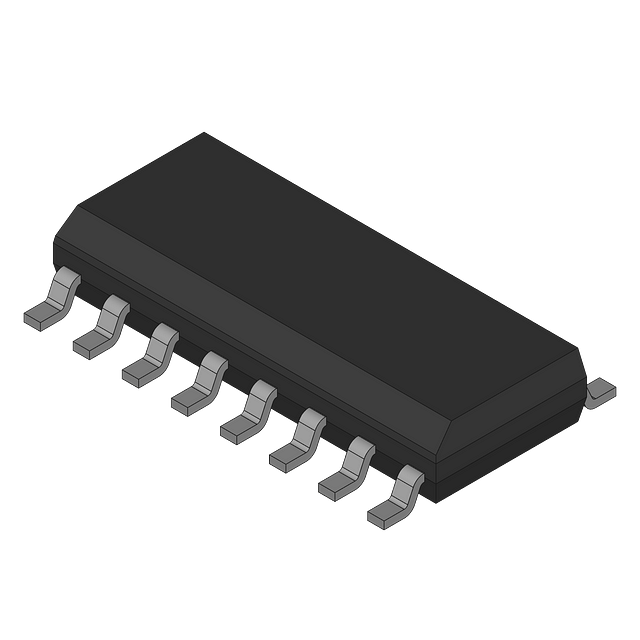
| 描述 | IC LED DRIVER RGBA 16SOICLED照明驱动器 4BIT I2C FM+ TP LED CON RST OE |
| 产品分类 | |
| 品牌 | NXP Semiconductors |
| 产品手册 | |
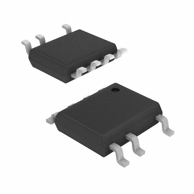
| 产品图片 |
|
| rohs | 符合RoHS无铅 / 符合限制有害物质指令(RoHS)规范要求 |
| 产品系列 | LED照明电子器件,LED照明驱动器,NXP Semiconductors PCA9633D16,118- |
| 数据手册 | |
| 产品型号 | PCA9633D16,118 |
| 产品种类 | LED照明驱动器 |
| 低电平输出电流 | 25 mA |
| 供应商器件封装 | 16-SO |
| 其它名称 | 568-8716-6 |
| 内部驱动器 | 两者兼有 |
| 功率耗散 | 400 mW |
| 包装 | Digi-Reel® |
| 商标 | NXP Semiconductors |
| 安装类型 | 表面贴装 |
| 安装风格 | SMD/SMT |
| 封装 | Reel |
| 封装/外壳 | 16-SOIC(0.154",3.90mm 宽) |
| 封装/箱体 | SO-16 |
| 工作温度 | -40°C ~ 85°C |
| 工厂包装数量 | 2500 |
| 恒压 | - |
| 恒流 | - |
| 拓扑 | 开路漏极,PWM |
| 最大工作温度 | + 85 C |
| 最大电源电流 | 10 mA |
| 最小工作温度 | - 40 C |
| 标准包装 | 1 |
| 电压-电源 | 2.3 V ~ 5.5 V |
| 电压-输出 | 5.5V |
| 类型-初级 | 背光,LED 闪烁器 |
| 类型-次级 | RGBA |
| 输入电压 | 2.3 V to 5.5 V |
| 输出数 | 4 |
| 零件号别名 | PCA9633D16-T |
| 频率 | 25MHz |
| 高电平输出电流 | 50 uA |


- 商务部:美国ITC正式对集成电路等产品启动337调查
- 曝三星4nm工艺存在良率问题 高通将骁龙8 Gen1或转产台积电
- 太阳诱电将投资9.5亿元在常州建新厂生产MLCC 预计2023年完工
- 英特尔发布欧洲新工厂建设计划 深化IDM 2.0 战略
- 台积电先进制程称霸业界 有大客户加持明年业绩稳了
- 达到5530亿美元!SIA预计今年全球半导体销售额将创下新高
- 英特尔拟将自动驾驶子公司Mobileye上市 估值或超500亿美元
- 三星加码芯片和SET,合并消费电子和移动部门,撤换高东真等 CEO
- 三星电子宣布重大人事变动 还合并消费电子和移动部门
- 海关总署:前11个月进口集成电路产品价值2.52万亿元 增长14.8%


PDF Datasheet 数据手册内容提取
PCA9633 4-bit Fm+ I2C-bus LED driver Rev. 05 — 25 July 2008 Product data sheet 1. General description The PCA9633 is an I2C-bus controlled 4-bit LED driver optimized for Red/Green/Blue/Amber (RGBA) color mixing applications. Each LED output has its own 8-bit resolution (256 steps) fixed frequency IndividualPWM controller that operates at 97kHz with a duty cycle that is adjustable from 0% to 99.6% to allow the LED to be set to a specific brightness value. A fifth 8-bit resolution (256steps) GroupPWM controller hasbothafixedfrequencyof190Hzandanadjustablefrequencybetween24Hztoonce every10.73secondswithadutycyclethatisadjustablefrom0%to99.6%thatisusedto either dim or blink all LEDs with the same value. Each LED output can be off, on (no PWM control), set at its IndividualPWM controller value or at both Individual and Group PWM controller values. The LED output driver is programmed to be either open-drain with a 25mA current sink capability at 5V or totem pole with a 25mA sink, 10mA source capability at 5V. The PCA9633 operates with a supply voltage range of 2.3V to 5.5V and the outputs are 5.5V tolerant. LEDs can be directly connected to the LED output (up to 25mA, 5.5V) or controlled with external driversandaminimumamountofdiscretecomponentsforlargercurrentorhighervoltage LEDs. The PCA9633 is one of the first LED controller devices in a new Fast-mode Plus (Fm+) family.Fm+devicesofferhigherfrequency(upto1MHz)andmoredenselypopulatedbus operation (up to 4000pF). The activeLOW Output Enable input pin (OE) allows asynchronous control of the LED outputs and can be used to set all the outputs to a defined I2C-bus programmable logic state. TheOE can also be used to externally PWM the outputs, which is useful when multiple devices need to be dimmed or blinked together using software control. This feature is available for the 16-pin version only. SoftwareprogrammableLEDGroupandthreeSubCallI2Caddressesallowallordefined groups of PCA9633 devices to respond to a common I2C address, allowing for example, all red LEDs to be turned on or off at the same time or marquee chasing effect, thus minimizing I2C-bus commands. The PCA9633 is offered with 3 different I2C-bus address options: fixed I2C-bus address (8-pin version), 4 different I2C-bus addresses from 2 programmable address pins (10-pin version), and 126 different I2C-bus addresses from 7 programmable address pins (16-pin version). They are software identical except for the different number of address combinations. The Software Reset (SWRST) Call allows the master to perform a reset of the PCA9633 throughtheI2C-bus,identicaltothePower-OnReset(POR)thatinitializestheregistersto their default state causing the outputs to be set HIGH (LED off). This allows an easy and quick way to reconfigure all device registers to the same condition.
PCA9633 NXP Semiconductors 4-bit Fm+ I2C-bus LED driver 2. Features n 4 LED drivers. Each output programmable at: u Off u On u Programmable LED brightness u Programmable group dimming/blinking mixed with individual LED brightness n 1MHz Fast-mode Plus I2C-bus interface with 30mA high drive capability on SDA output for driving high capacitive buses n 256-step (8-bit) linear programmable brightness per LED output varying from fully off (default) to maximum brightness using a 97kHz PWM signal n 256-step group brightness control allows general dimming (using a 190Hz PWM signal) from fully off to maximum brightness (default) n 256-step group blinking with frequency programmable from 24Hz to 10.73s and dutycycle from 0% to 99.6% n Four totem pole outputs (sink 25mA and source 10mA at 5V) with software programmable open-drain LED outputs selection (default at totem pole). No input function. n Output state change programmable on the Acknowledge or the STOP Command to update outputs byte-by-byte or all at the same time (default to ‘Change on STOP’). n Active LOW Output Enable (OE) input pin. LED outputs programmable to ‘1’, ‘0’ or ‘high-impedance’ (default at power-up) whenOE is HIGH, thus allowing hardware blinking and dimming of the LEDs (16-pin version only). n 2 hardware address pins (10-pin version) and 7 hardware address pins (16-pin version) allow respectively up to 4 and 126 devices to be connected to the same I2C-bus. No hardware address pins in the 8-pin version. n 4 software programmable I2C-bus addresses (one LED Group Call address and three LEDSubCalladdresses)allowgroupsofdevicestobeaddressedatthesametimein anycombination(forexample,oneregisterusedfor‘AllCall’sothatallthePCA9633s on the I2C-bus can be addressed at the same time and the second register used for three different addresses so that1⁄ of all devices on the bus can be addressed at the 3 same time in a group). Software enable and disable for I2C-bus address. n Software Reset feature (SWRST Call) allows the device to be reset through the I2C-bus n 25MHz internal oscillator requires no external components n Internal power-on reset n Noise filter on SDA/SCL inputs n Edge rate control on outputs n No glitch on power-up n Supports hot insertion n Low standby current n Operating power supply voltage range of 2.3V to 5.5V n 5.5V tolerant inputs n - 40(cid:176) C to +85(cid:176) C operation n ESD protection exceeds 2000V HBM per JESD22-A114, 200V MM per JESD22-A115, and 1000V CDM per JESD22-C101 n Latch-up testing is done to JEDEC Standard JESD78 which exceeds 100mA PCA9633_5 © NXP B.V. 2008. All rights reserved. Product data sheet Rev. 05 — 25 July 2008 2 of 43
PCA9633 NXP Semiconductors 4-bit Fm+ I2C-bus LED driver n Packages offered: SO, TSSOP (MSOP), HVQFN, HVSON 3. Applications n RGB or RGBA LED drivers n LED status information n LED displays n LCD backlights n Keypad backlights for cellular phones or handheld devices 4. Ordering information Table 1. Ordering information Type number Topside Package mark Name Description Version PCA9633D16 PCA9633 SO16 plastic small outline package; 16 leads; body width 3.9mm SOT109-1 PCA9633DP1 9633 TSSOP8 plastic thin shrink small outline package; 8 leads; SOT505-1 bodywidth3mm PCA9633DP2 9633 TSSOP10 plastic thin shrink small outline package; 10 leads; SOT552-1 bodywidth3mm PCA9633PW PCA9633 TSSOP16 plastic thin shrink small outline package; 16 leads; SOT403-1 bodywidth4.4mm PCA9633BS 9633 HVQFN16 plasticthermalenhancedverythinquadflatpackage;noleads; SOT629-1 16terminals; body 4· 4· 0.85mm PCA9633TK 9633 HVSON8 plastic thermal enhanced very thin small outline package; SOT908-1 noleads; 8terminals; body 3· 3· 0.85mm PCA9633_5 © NXP B.V. 2008. All rights reserved. Product data sheet Rev. 05 — 25 July 2008 3 of 43
PCA9633 NXP Semiconductors 4-bit Fm+ I2C-bus LED driver 5. Block diagram 16-pin version 10-pin version A0 A1 A2 A3 A4 A5 A6 PCA9633 SCL INPUT FILTER SDA I2C-BUS CONTROL POWER-ON VDD RESET VDD VSS LED STATE SELECT REGISTER PWM REGISTER X BRIGHTNESS LEDn CONTROL 97 kHz 24.3 kHz GRPFREQ MUX/ CONTROL REGISTER GRPPWM 25 MHz REGISTER OSCILLATOR 190 Hz '0' – permanently OFF '1' – permanently ON OE (16-pin version only) 002aab283 Fig 1. Block diagram of PCA9633 PCA9633_5 © NXP B.V. 2008. All rights reserved. Product data sheet Rev. 05 — 25 July 2008 4 of 43
PCA9633 NXP Semiconductors 4-bit Fm+ I2C-bus LED driver 6. Pinning information 6.1 Pinning LED0 1 10 VDD LED0 1 8 VDD LED1 2 9 SDA LED1 2 7 SDA PCA9633DP1 LED2 3 PCA9633DP2 8 SCL LED2 3 6 SCL LED3 4 7 A1 LED3 4 5 VSS A0 5 6 VSS 002aab314 002aab315 Fig 2. Pin configuration for TSSOP8 Fig 3. Pin configuration for TSSOP10 A0 1 16 VDD A1 2 15 A6 LED0 3 14 A5 A0 1 16 VDD A1 2 15 A6 LED1 4 13 SDA PCA9633D16 LED0 3 14 A5 LED2 5 12 SCL LED1 4 13 SDA PCA9633PW LED2 5 12 SCL LED3 6 11 A4 LED3 6 11 A4 A2 7 10 OE A2 7 10 OE A3 8 9 VSS A3 8 9 VSS 002aab316 002aab313 Fig 4. Pin configuration for TSSOP16 Fig 5. Pin configuration for SO16 D terminal 1 1 0 D 6 A A V A index area 6 5 4 3 terminal 1 1 1 1 1 index area LED0 1 12 A5 LED0 1 8 VDD LED1 2 11 SDA PCA9633BS LED1 2 7 SDA LED2 3 10 SCL PCA9633TK LED3 4 9 A4 LED2 3 6 SCL 5 6 7 8 LED3 4 5 VSS 2 3 S E A A S O 002aab317 V 002aab807 Transparent top view Transparent top view Fig 6. Pin configuration for HVQFN16 Fig 7. Pin configuration for HVSON8 PCA9633_5 © NXP B.V. 2008. All rights reserved. Product data sheet Rev. 05 — 25 July 2008 5 of 43
PCA9633 NXP Semiconductors 4-bit Fm+ I2C-bus LED driver 6.2 Pin description Table 2. Pin description for TSSOP8 and HVSON8 Symbol Pin Type Description LED0 1 O LED driver 0 LED1 2 O LED driver 1 LED2 3 O LED driver 2 LED3 4 O LED driver 3 V 5 power supply supply ground SS SCL 6 I serial clock line SDA 7 I/O serial data line V 8 power supply supply voltage DD Table 3. Pin description for TSSOP10 Symbol Pin Type Description LED0 1 O LED driver 0 LED1 2 O LED driver 1 LED2 3 O LED driver 2 LED3 4 O LED driver 3 A0 5 I address input 0 V 6 power supply supply ground SS A1 7 I address input 1 SCL 8 I serial clock line SDA 9 I/O serial data line V 10 power supply supply voltage DD PCA9633_5 © NXP B.V. 2008. All rights reserved. Product data sheet Rev. 05 — 25 July 2008 6 of 43
PCA9633 NXP Semiconductors 4-bit Fm+ I2C-bus LED driver Table 4. Pin description for SO16 and TSSOP16 Symbol Pin Type Description A0 1 I address input 0 A1 2 I address input 1 LED0 3 O LED driver 0 LED1 4 O LED driver 1 LED2 5 O LED driver 2 LED3 6 O LED driver 3 A2 7 I address input 2 A3 8 I address input 3 V 9 power supply supply ground SS OE 10 I active LOW Output Enable A4 11 I address input 4 SCL 12 I serial clock line SDA 13 I/O serial data line A5 14 I address input 5 A6 15 I address input 6 V 16 power supply supply voltage DD Table 5. Pin description for HVQFN16 Symbol Pin Type Description LED0 1 O LED driver 0 LED1 2 O LED driver 1 LED2 3 O LED driver 2 LED3 4 O LED driver 3 A2 5 I address input 2 A3 6 I address input 3 V [1] 7 power supply supply ground SS OE 8 I active LOW Output Enable A4 9 I address input 4 SCL 10 I serial clock line SDA 11 I/O serial data line A5 12 I address input 5 A6 13 I address input 6 V 14 power supply supply voltage DD A0 15 I address input 0 A1 16 I address input 1 [1] HVQFN16 package die supply ground is connected to both the V pin and the exposed center pad. The SS V pinmustbeconnectedtosupplygroundforproperdeviceoperation.Forenhancedthermal,electrical, SS and board-level performance, the exposed pad needs to be soldered to the board using a corresponding thermal pad on the board, and for proper heat conduction through the board thermal vias need to be incorporated in the PCB in the thermal pad region. PCA9633_5 © NXP B.V. 2008. All rights reserved. Product data sheet Rev. 05 — 25 July 2008 7 of 43
PCA9633 NXP Semiconductors 4-bit Fm+ I2C-bus LED driver 7. Functional description Refer toFigure 1 “Block diagram of PCA9633”. 7.1 Device addresses Following a START condition, the bus master must output the address of the slave it is accessing. There are a maximum of 128 possible programmable addresses using the 7 hardware address pins. Two of these addresses, Software Reset and LED All Call, cannot be used because their default power-up state is ON, leaving a maximum of 126 addresses. Using other reserved addresses, as well as any other subcall address, will reduce the total number of possible addresses even further. 7.1.1 Regular I2C-bus slave address The I2C-bus slave address of the PCA9633 is shown inFigure8. To conserve power, no internal pull-up resistors are incorporated on the hardware selectable address pins and they must be pulled HIGH or LOW (10-pin and 16-pin versions). Remark:UsingreservedI2C-busaddresseswillinterferewithotherdevices,butonlyifthe devicesareonthebusand/orthebuswillbeopentootherI2C-bussystemsatsomelater date. In a closed system where the designer controls the address assignment these addresses can be used since the PCA9633 treats them like any other address. The LEDAllCall,SoftwareResetandPCA9564orPCA9665slaveaddress(ifonthebus)can never be used for individual device addresses. • PCA9633 LED All Call address (1110000) and Software Reset (00000110) which are active on start-up • PCA9564 (0000000) or PCA9665 (1110000) slave address which is active on start-up • ‘reserved for future use’ I2C-bus addresses (0000011, 11111XX) • slave devices that use the 10-bit addressing scheme (11110XX) • slave devices that are designed to respond to the General Call address (0000000) • High-speed mode (Hs-mode) master code (00001XX). slave address slave address slave address 1 1 0 0 0 A1 A0 R/W 1 1 0 0 0 1 0 R/W A6 A5 A4 A3 A2 A1 A0 R/W fixed hardware selectable fixed hardware selectable 002aab318 002aab295 002aab319 a. 8-pin version b. 10-pin version c. 16-pin version Fig 8. Slave address Thelastbitoftheaddressbytedefinestheoperationtobeperformed.Whensettologic1 a read is selected, while a logic0 selects a write operation. PCA9633_5 © NXP B.V. 2008. All rights reserved. Product data sheet Rev. 05 — 25 July 2008 8 of 43
PCA9633 NXP Semiconductors 4-bit Fm+ I2C-bus LED driver 7.1.2 LED All Call I2C-bus address • Default power-up value (ALLCALLADR register): E0h or 1110000X • Programmable through I2C-bus (volatile programming) • Atpower-up,LEDAllCallI2C-busaddressisenabled.PCA9633sendsanACKwhen E0h (R/W=0) or E1h (R/W=1) is sent by the master. SeeSection 7.3.8 “LED All Call I2C-bus address, ALLCALLADR” for more detail. Remark:ThedefaultLEDAllCallI2C-busaddress(E0hor1110000X)mustnotbeused as a regular I2C-bus slave address since this address is enabled at power-up. All the PCA9633s on the I2C-bus will acknowledge the address if sent by the I2C-bus master. 7.1.3 LED Sub Call I2C-bus addresses • 3 different I2C-bus addresses can be used • Default power-up values: – SUBADR1 register: E2h or 1110001X – SUBADR2 register: E4h or 1110010X – SUBADR3 register: E8h or 1110100X • Programmable through I2C-bus (volatile programming) • At power-up, Sub Call I2C-bus addresses are disabled. PCA9633 does not send an ACK when E2h (R/W=0) or E3h (R/W=1), E4h (R/W=0) or E5h (R/W=1), or E8h(R/W=0) or E9h (R/W=1) is sent by the master. SeeSection 7.3.7 “I2C-bus subaddress 1to3, SUBADRx” for more detail. Remark:The default LED Sub Call I2C-bus addresses may be used as regular I2C-bus slave addresses as long as they are disabled. 7.1.4 Software Reset I2C-bus address The address shown inFigure9 is used when a reset of the PCA9633 needs to be performed by the master. The Software Reset address (SWRST Call) must be used with R/W=0. If R/W=1, the PCA9633 does not acknowledge the SWRST. SeeSection 7.6 “Software Reset” for more detail. R/W 0 0 0 0 0 1 1 0 002aab416 Fig 9. Software Reset address Remark:TheSoftwareResetI2C-busaddressisareservedaddressandcannotbeused asaregularI2C-busslaveaddress(16-pinversion)orasanLEDAllCallorLEDSubCall address. PCA9633_5 © NXP B.V. 2008. All rights reserved. Product data sheet Rev. 05 — 25 July 2008 9 of 43
PCA9633 NXP Semiconductors 4-bit Fm+ I2C-bus LED driver 7.2 Control register Following the successful acknowledgement of the slave address, LED All Call address or LED Sub Call address, the bus master will send a byte to the PCA9633, which will be stored in the Control register. The lowest 4bits are used as a pointer to determine which register will be accessed (D[3:0]). The highest 3bits are used as Auto-Increment flag and Auto-Increment options (AI[2:0]). Bit4 is unused and must be programmed with zero (0) for proper device operation. register address AI2 AI1 AI0 0 D3 D2 D1 D0 002aab296 Auto-Increment options Auto-Increment flag reset state = 80h Remark:The Control register does not apply to the Software Reset I2C-bus address. Fig 10. Control register When the Auto-Increment flag is set (AI2=1), the four low order bits of the Control register are automatically incremented after a read or write. This allows the user to program the registers sequentially. Four different types of Auto-Increment are possible, depending on AI1 and AI0 values. Table 6. Auto-Increment options AI2 AI1 AI0 Function 0 0 0 no Auto-Increment 1 0 0 Auto-Increment for all registers. D3, D2, D1, D0 roll over to ‘0000’ after the last register (1100) is accessed. 1 0 1 Auto-Increment for individual brightness registers only. D3, D2, D1, D0 roll over to ‘0010’ after the last register (0101) is accessed. 1 1 0 Auto-Increment for global control registers only. D3, D2, D1, D0 roll over to ‘0110’ after the last register (0111) is accessed. 1 1 1 Auto-Increment for individual and global control registers only. D3, D2, D1, D0 roll over to ‘0010’ after the last register (0111) is accessed. Remark:Other combinations not shown inTable6 (AI[2:0] = 001, 010, and 011) are reserved and must not be used for proper device operation. AI[2:0]=000 is used when the same register must be accessed several times during a singleI2C-buscommunication,forexample,changesthebrightnessofasingleLED.Data is overwritten each time the register is accessed during a write operation. AI[2:0]=100 is used when all the registers must be sequentially accessed, for example, power-up programming. AI[2:0]=101 is used when the four LED drivers must be individually programmed with different values during the same I2C-bus communication, for example, changing color setting to another color setting. PCA9633_5 © NXP B.V. 2008. All rights reserved. Product data sheet Rev. 05 — 25 July 2008 10 of 43
PCA9633 NXP Semiconductors 4-bit Fm+ I2C-bus LED driver AI[2:0]=110 is used when the LED drivers must be globally programmed with different settings during the same I2C-bus communication, for example, global brightness or blinking change. AI[2:0]=111 is used when individual and global changes must be performed during the sameI2C-buscommunication,forexample,changingacolorandglobalbrightnessatthe same time. Only the 4 least significant bits D[3:0] are affected by the AI[2:0] bits. When the Control register is written, the register entry point determined by D[3:0] is the first register that will be addressed (read or write operation), and can be anywhere between 0000 and 1100 (as defined inTable7). When AI[2]=1, the Auto-Increment flag is set and the rollover value at which the point where the register increment stops and goes to the next one is determined by AI[2:0]. SeeTable6 for rollover values. For example,iftheControlregister=11101000(E8h),thentheregisteraddressingsequence will be (in hex): 08fi …fi 0Cfi 00fi …fi 07fi 02fi …fi 07fi 02fi …fi 07fi 02fi … as long as the master keeps sending or reading data. 7.3 Register definitions Table 7. Register summary[1][2] Register number (hex) D3 D2 D1 D0 Name Type Function 00h 0 0 0 0 MODE1 read/write Mode register 1 01h 0 0 0 1 MODE2 read/write Mode register 2 02h 0 0 1 0 PWM0 read/write brightness control LED0 03h 0 0 1 1 PWM1 read/write brightness control LED1 04h 0 1 0 0 PWM2 read/write brightness control LED2 05h 0 1 0 1 PWM3 read/write brightness control LED3 06h 0 1 1 0 GRPPWM read/write group duty cycle control 07h 0 1 1 1 GRPFREQ read/write group frequency 08h 1 0 0 0 LEDOUT read/write LED output state 09h 1 0 0 1 SUBADR1 read/write I2C-bus subaddress 1 0Ah 1 0 1 0 SUBADR2 read/write I2C-bus subaddress 2 0Bh 1 0 1 1 SUBADR3 read/write I2C-bus subaddress 3 0Ch 1 1 0 0 ALLCALLADR read/write LED All Call I2C-bus address [1] Only D[3:0]=0000to1100 are allowed and will be acknowledged. D[3:0]=1101, 1110, or 1111 are reserved and will not be acknowledged. [2] When writing to the Control register, bit4 must be programmed with logic0 for proper device operation. PCA9633_5 © NXP B.V. 2008. All rights reserved. Product data sheet Rev. 05 — 25 July 2008 11 of 43
PCA9633 NXP Semiconductors 4-bit Fm+ I2C-bus LED driver 7.3.1 Mode register 1, MODE1 Table 8. MODE1 - Mode register 1 (address 00h) bit description Legend: * default value. Bit Symbol Access Value Description 7 AI2 read only 0 Register Auto-Increment disabled 1* Register Auto-Increment enabled 6 AI1 read only 0* Auto-Increment bit1=0 1 Auto-Increment bit1=1 5 AI0 read only 0* Auto-Increment bit0=0 1 Auto-Increment bit0=1 4 SLEEP R/W 0 Normal mode[1]. 1* Low power mode. Oscillator off[2]. 3 SUB1 R/W 0* PCA9633 does not respond to I2C-bus subaddress 1. 1 PCA9633 responds to I2C-bus subaddress 1. 2 SUB2 R/W 0* PCA9633 does not respond to I2C-bus subaddress 2. 1 PCA9633 responds to I2C-bus subaddress 2. 1 SUB3 R/W 0* PCA9633 does not respond to I2C-bus subaddress 3. 1 PCA9633 responds to I2C-bus subaddress 3. 0 ALLCALL R/W 0 PCA9633 does not respond to LED All Call I2C-bus address. 1* PCA9633 responds to LED All Call I2C-bus address. [1] It takes 500m s max. for the oscillator to be up and running once SLEEP bit has been set to logic0. Timings on LEDn outputs are not guaranteed if PWMx, GRPPWM or GRPFREQ registers are accessed within the 500m s window. [2] When the oscillator is off (Sleep mode) the LED outputs cannot be turned on, off or dimmed/blinked. 7.3.2 Mode register 2, MODE2 Table 9. MODE2 - Mode register 2 (address 01h) bit description Legend: * default value. Bit Symbol Access Value Description 7 - read only 0* reserved 6 - read only 0* reserved 5 DMBLNK R/W 0* Group control = dimming 1 Group control = blinking 4 INVRT[1] R/W 0* Output logic state not inverted. Value to use when no external driver used. Applicable whenOE=0 for PCA9633 16-pin version. 1 Output logic state inverted. Value to use when external driver used. Applicable whenOE=0 for PCA9633 16-pin version. 3 OCH R/W 0* Outputs change on STOP command.[2] 1 Outputs change on ACK. 2 OUTDRV[1] R/W 0 The 4 LED outputs are configured with an open-drain structure. 1* The 4 LED outputs are configured with a totem pole structure. PCA9633_5 © NXP B.V. 2008. All rights reserved. Product data sheet Rev. 05 — 25 July 2008 12 of 43
PCA9633 NXP Semiconductors 4-bit Fm+ I2C-bus LED driver Table 9. MODE2 - Mode register 2 (address 01h) bit description …continued Legend: * default value. Bit Symbol Access Value Description 1to0 OUTNE[1:0] R/W 00 WhenOE = 1 (output drivers not enabled), LEDn = 0. [3][4] 01* WhenOE = 1 (output drivers not enabled): LEDn = 1 when OUTDRV=1 LEDn=high-impedance when OUTDRV=0 (same as OUTNE[1:0]=10) 10 WhenOE = 1 (output drivers not enabled), LEDn = high-impedance. 11 reserved [1] SeeSection 7.7 “Using the PCA9633 with and without external drivers” for more details. Normal LEDs can be driven directly in either mode.SomenewerLEDsincludeintegratedZenerdiodestolimitvoltagetransients,reduceEMIandprotecttheLEDs,andthesemust be driven only in the open-drain mode to prevent overheating the IC. [2] Change of the outputs at the STOP command allows synchronizing outputs of more than one PCA9633. Applicable to registers from 02h (PWM0) to 08h (LEDOUT) only. [3] SeeSection 7.4 “Active LOW output enable input” for more details. [4] OUTNE[1:0] is only for PCA9633 16-pin version. 7.3.3 PWM registers 0 to 3, PWMx — Individual brightness control registers Table 10. PWM0toPWM3 - PWM registers 0to3 (address 02h to 05h) bit description Legend: * default value. Address Register Bit Symbol Access Value Description 02h PWM0 7:0 IDC0[7:0] R/W 00000000* PWM0 Individual Duty Cycle 03h PWM1 7:0 IDC1[7:0] R/W 00000000* PWM1 Individual Duty Cycle 04h PWM2 7:0 IDC2[7:0] R/W 00000000* PWM2 Individual Duty Cycle 05h PWM3 7:0 IDC3[7:0] R/W 00000000* PWM3 Individual Duty Cycle A 97kHz fixed frequency signal is used for each output. Duty cycle is controlled through 256 linear steps from 00h (0% duty cycle = LED output off) to FFh (99.6%dutycycle=LED output at maximum brightness). Applicable to LED outputs programmed with LDRx=10 or 11 (LEDOUT register). IDC[7:0] duty cycle = ------------------------ (1) 256 7.3.4 Group duty cycle control, GRPPWM Table 11. GRPPWM - Group duty cycle control register (address 06h) bit description Legend: * default value. Address Register Bit Symbol Access Value Description 06h GRPPWM 7:0 GDC[7:0] R/W 11111111 GRPPWM register When DMBLNK bit (MODE2 register) is programmed with 0, a 190Hz fixed frequency signal is superimposed with the 97kHz individual brightness control signal. GRPPWM is then used as a global brightness control allowing the LED outputs to be dimmed with the same value. The value in GRPFREQ is then a ‘Don’t care’. General brightness for the 4 outputs is controlled through 256 linear steps from 00h (0%duty cycle=LED output off) to FFh (99.6% duty cycle=maximum brightness). Applicable to LED outputs programmed with LDRx=11 (LEDOUT register). PCA9633_5 © NXP B.V. 2008. All rights reserved. Product data sheet Rev. 05 — 25 July 2008 13 of 43
PCA9633 NXP Semiconductors 4-bit Fm+ I2C-bus LED driver When DMBLNK bit is programmed with 1, GRPPWM and GRPFREQ registers define a global blinking pattern, where GRPFREQ contains the blinking period (from 24Hz to 10.73s) and GRPPWM the duty cycle (ON/OFF ratio in%). GDC[7:0] duty cycle = --------------------------- (2) 256 7.3.5 Group frequency, GRPFREQ Table 12. GRPFREQ - Group Frequency register (address 07h) bit description Legend: * default value. Address Register Bit Symbol Access Value Description 07h GRPFREQ 7:0 GFRQ[7:0] R/W 00000000* GRPFREQ register GRPFREQ is used to program the global blinking period when DMBLNK bit (MODE2 register) is equal to 1. Value in this register is a ‘Don’t care’ when DMBLNK=0. Applicable to LED outputs programmed with LDRx=11 (LEDOUT register). Blinking period is controlled through 256 linear steps from 00h (41ms, frequency 24Hz) to FFh (10.73s). GFRQ[7:0]+1 global blinking period = ---------------------------------------- (in seconds) (3) 24 7.3.6 LED driver output state, LEDOUT Table 13. LEDOUT - LED driver output state register (address 08h) bit description Legend: * default value. Address Register Bit Symbol Access Value Description 08h LEDOUT 7:6 LDR3 R/W 00* LED3 output state control 5:4 LDR2 R/W 00* LED2 output state control 3:2 LDR1 R/W 00* LED1 output state control 1:0 LDR0 R/W 00* LED0 output state control LDRx=00 —LED driver x is off (default power-up state). LDRx=01 —LED driver x is fully on (individual brightness and group dimming/blinking not controlled). LDRx=10 —LED driver x individual brightness can be controlled through its PWMx register. LDRx=11 —LED driver x individual brightness and group dimming/blinking can be controlled through its PWMx register and the GRPPWM registers. PCA9633_5 © NXP B.V. 2008. All rights reserved. Product data sheet Rev. 05 — 25 July 2008 14 of 43
PCA9633 NXP Semiconductors 4-bit Fm+ I2C-bus LED driver 7.3.7 I2C-bus subaddress 1 to 3, SUBADRx Table 14. SUBADR1toSUBADR3 - I2C-bus subaddress registers 0to3 (address 09h to 0Bh) bit description Legend: * default value. Address Register Bit Symbol Access Value Description 09h SUBADR1 7:1 A1[7:1] R/W 1110001* I2C-bus subaddress 1 0 A1[0] R only 0* reserved 0Ah SUBADR2 7:1 A2[7:1] R/W 1110010* I2C-bus subaddress 2 0 A2[0] R only 0* reserved 0Bh SUBADR3 7:1 A3[7:1] R/W 1110100* I2C-bus subaddress 3 0 A3[0] R only 0* reserved Subaddresses are programmable through the I2C-bus. Default power-up values are E2h, E4h, E8h, and the device(s) will not acknowledge these addresses right after power-up (the corresponding SUBx bit in MODE1 register is equal to 0). Once subaddresses have been programmed to their right values, SUBx bits need to be set to 1 in order to have the device acknowledging these addresses (MODE1 register). Only the 7MSBs representing the I2C-bus subaddress are valid. The LSB in SUBADRx register is a read-only bit (0). When SUBx is set to 1, the corresponding I2C-bus subaddress can be used during either an I2C-bus read or write sequence. 7.3.8 LED All Call I2C-bus address, ALLCALLADR Table 15. ALLCALLADR - LED All Call I2C-bus address register (address 0Ch) bit description Legend: * default value. Address Register Bit Symbol Access Value Description 0Ch ALLCALLADR 7:1 AC[7:1] R/W 1110000* ALLCALL I2C-bus address register 0 AC[0] R only 0* reserved The LED All Call I2C-bus address allows all the PCA9633s in the bus to be programmed at the same time (ALLCALL bit in register MODE1 must be equal to 1, power-up default state). This address is programmable through the I2C-bus and can be used during either an I2C-bus read or write sequence. The register address can be programmed as a subcall. Only the 7MSBs representing the All Call I2C-bus address are valid. The LSB in ALLCALLADR register is a Read-only bit (0). IfALLCALLbit=0,thedevicedoesnotacknowledgetheaddressprogrammedinregister ALLCALLADR. PCA9633_5 © NXP B.V. 2008. All rights reserved. Product data sheet Rev. 05 — 25 July 2008 15 of 43
PCA9633 NXP Semiconductors 4-bit Fm+ I2C-bus LED driver 7.4 Active LOW output enable input TheactiveLOWoutputenable(OE)pin,allowstoenableordisablealltheLEDoutputsat the same time. This control signal is only available for the 16-pin version and does not apply to the 8-pin or 10-pin versions. • WhenaLOWlevelisappliedtoOEpin,alltheLEDoutputsareenabledandfollowthe output state defined in the LEDOUT register with the polarity defined by INVRT bit (MODE2 register). • When a HIGH level is applied toOE pin, all the LED outputs are programmed to the value that is defined by OUTNE[1:0] in the MODE2 register. Table 16. LED outputs whenOE=1 OUTNE1 OUTNE0 LED outputs 0 0 0 0 1 1 if OUTDRV=1, high-impedance if OUTDRV=0 1 0 high-impedance 1 1 reserved TheOE pin can be used as a synchronization signal to switch on/off several PCA9633 devices at the same time. This requires an external clock reference that provides blinking period and the duty cycle. TheOEpincanalsobeusedasanexternaldimmingcontrolsignal.Thefrequencyofthe external clock must be high enough not to be seen by the human eye, and the duty cycle value determines the brightness of the LEDs. Remark:Do not useOE as an external blinking control signal when internal global blinking is selected (DMBLNK=1, MODE2 register) since it will result in an undefined blinkingpattern.DonotuseOEasanexternaldimmingcontrolsignalwheninternalglobal dimming is selected (DMBLNK=0, MODE2 register) since it will result in an undefined dimming pattern. 7.5 Power-on reset When power is applied to V , an internal Power-on reset holds the PCA9633 in a reset DD conditionuntilV hasreachedV .Atthispoint,theresetconditionisreleasedandthe DD POR PCA9633 registers and I2C-bus state machine are initialized to their default states (all zeroes)causingallthechannelstobedeselected.Thereafter,V mustbeloweredbelow DD 0.2V to reset the device. PCA9633_5 © NXP B.V. 2008. All rights reserved. Product data sheet Rev. 05 — 25 July 2008 16 of 43
PCA9633 NXP Semiconductors 4-bit Fm+ I2C-bus LED driver 7.6 Software Reset TheSoftwareResetCall(SWRSTCall)allowsallthedevicesintheI2C-bustoberesetto thepower-upstatevaluethroughaspecificformattedI2C-buscommand.Tobeperformed correctly, it implies that the I2C-bus is functional and that there is no device hanging the bus. The SWRST Call function is defined as the following: 1. A START command is sent by the I2C-bus master. 2. The reserved SWRST I2C-bus address ‘0000011’ with the R/W bit set to 0 (write) is sent by the I2C-bus master. 3. The PCA9633 device(s) acknowledge(s) after seeing the SWRST Call address ‘00000110’(06h)only.IftheR/Wbitissetto1(read),noacknowledgeisreturnedto the I2C-bus master. 4. Once the SWRST Call address has been sent and acknowledged, the master sends 2bytes with 2 specific values (SWRST data byte1 and byte2): a. Byte 1=A5h: the PCA9633 acknowledges this value only. If byte1 is not equal to A5h, the PCA9633 does not acknowledge it. b. Byte 2=5Ah: the PCA9633 acknowledges this value only. If byte2 is not equal to 5Ah, then the PCA9633 does not acknowledge it. If more than 2bytes of data are sent, the PCA9633 does not acknowledge any more. 5. Once the right 2bytes (SWRST data byte1 and byte2 only) have been sent and correctlyacknowledged,themastersendsaSTOPcommandtoendtheSWRSTCall: the PCA9633 then resets to the default value (power-up value) and is ready to be addressed again within the specified bus free time (t ). BUF TheI2C-busmastermustinterpretanon-acknowledgefromthePCA9633(atanytime)as a ‘SWRST Call Abort’. The PCA9633 does not initiate a reset of its registers. This happens only when the format of the SWRST Call sequence is not correct. PCA9633_5 © NXP B.V. 2008. All rights reserved. Product data sheet Rev. 05 — 25 July 2008 17 of 43
PCA9633 NXP Semiconductors 4-bit Fm+ I2C-bus LED driver 7.7 Using the PCA9633 with and without external drivers The PCA9633 LED output drivers are 5.5V only tolerant and can sink up to 25mA at 5V. If the device needs to drive LEDs to a higher voltage and/or higher current, use of an external driver is required. • INVRT bit (MODE2 register) can be used to keep the LED PWM control firmware the same(PWMxandGRPPWMvaluesdirectlycalculatedfromtheirrespectiveformulas andtheLEDoutputstatedeterminedbyLEDOUTregistervalue)independentlyofthe typeofexternaldriver.ThisbitallowsLEDoutputpolarityinversion/non-inversiononly whenOE=0. • OUTDRVbit(MODE2register)allowsminimizingtheamountofexternalcomponents required to control the external driver (N-type or P-type device). Table 17. Use of INVRT and OUTDRV based on connection to the LEDn outputs whenOE=0[1] INVRT OUTDRV Direct connection to LEDn External N-type driver External P-type driver Firmware External Firmware External Firmware External pull-up pull-up pull-up resistor resistor resistor 0 0 formulas and LED LEDcurrent formulasandLED required formulas and LED required output state values limiting R[2] output state outputstatevalues apply[2] values inverted apply 0 1 formulas and LED LEDcurrent formulasandLED not required formulas and LED not output state values limiting R[2] output state outputstatevalues required[4] apply[2] values inverted apply[4] 1 0 formulas and LED LEDcurrent formulasandLED required formulas and LED required output state values limiting R output state outputstatevalues inverted values apply inverted 1 1 formulas and LED LEDcurrent formulasandLED not formulas and LED not required output state values limiting R output state required[3] outputstatevalues inverted values apply[3] inverted [1] OE applies to 16-pin version only. WhenOE=1, LED output state is controlled only by OUTNE[1:0] bits (MODE2 register). [2] Correct configuration when LEDs directly connected to the LEDn outputs (connection to V through current limiting resistor). DD [3] Optimum configuration when external N-type (NPN, NMOS) driver used. [4] Optimum configuration when external P-type (PNP, PMOS) driver used. PCA9633_5 © NXP B.V. 2008. All rights reserved. Product data sheet Rev. 05 — 25 July 2008 18 of 43
PCA9633 NXP Semiconductors 4-bit Fm+ I2C-bus LED driver Table 18. Output transistors based on LEDOUT registers, INVRT and OUTDRV bits whenOE=0[1] LEDOUT INVRT OUTDRV Upper transistor Lower transistor LEDn state (V to LEDn) (LEDn to V ) DD SS 00 0 0 off off high-Z[2] LED driver off 0 1 on off V DD 1 0 off on V SS 1 1 off on V SS 01 0 0 off on V SS LED driver on 0 1 off on V SS 1 0 off off high-Z[2] 1 1 on off V DD 10 0 0 off Individual PWM V or high-Z[2] = PWMx value SS Individual (non-inverted) brightness 0 1 Individual PWM Individual PWM V or V = PWMx value SS DD control (non-inverted) (non-inverted) 1 0 off Individual PWM high-Z[2] or V = 1- PWMx value SS (inverted) 1 1 Individual PWM Individual PWM V or V = 1- PWMx value DD SS (inverted) (inverted) 11 0 0 off Individual+Group V or high-Z[2] = PWMx/GRPPWM values SS Individual + PWM Group (non-inverted) dimming/blinking 0 1 Individual PWM Individual PWM V or V = PWMx/GRPPWM values SS DD (non-inverted) (non-inverted) 1 0 off Individual+Group high-Z[2] or V = (1- PWMx) or SS PWM (inverted) (1- GRPPWM) values 1 1 Individual PWM Individual PWM V or V =(1- PWMx) or DD SS (inverted) (inverted) (1- GRPPWM) values [1] OE applies to 16-pin version only. WhenOE=1, LED output state is controlled only by OUTNE[1:0] bits (MODE2 register). [2] External pull-up or LED current limiting resistor connects LEDn to V . DD PCA9633_5 © NXP B.V. 2008. All rights reserved. Product data sheet Rev. 05 — 25 July 2008 19 of 43
PCA9633 NXP Semiconductors 4-bit Fm+ I2C-bus LED driver 7.8 Individual brightness control with group dimming/blinking A 97kHz fixed frequency signal with programmable duty cycle (8 bits, 256 steps) is used to control individually the brightness for each LED. Ontopofthissignal,oneofthefollowingsignalscanbesuperimposed(thissignalcanbe applied to the 4 LED outputs): • A lower 190Hz fixed frequency signal with programmable duty cycle (8 bits, 256steps) is used to provide a global brightness control. • A programmable frequency signal from 24Hz to1⁄ Hz (8 bits, 256 steps) with 10.73 programmable duty cycle (8 bits, 256 steps) is used to provide a global blinking control. 508 510 512 1 2 3 4 5 6 7 8 9 10 11 12 507 509 511 1 2 3 4 5 6 7 8 9 10 11 Brightness Control signal (LEDn) N · 40 ns with N = (0 to 255) M · 256 · 2 · 40 ns (PWMx Register) with M = (0 to 255) (GRPPWM Register) 256 · 40 ns = 10.24 m s (97.6 kHz) Group Dimming signal 256 · 2 · 256 · 40 ns = 5.24 ms (190.7 Hz) 1 2 3 4 5 6 7 8 1 2 3 4 5 6 7 8 resulting Brightness + Group Dimming signal 002aab417 Minimum pulse width for LEDn Brightness Control is 40ns. Minimum pulse width for Group Dimming is 20.48m s. When M=1 (GRPPWM register value), the resulting LEDn Brightness Control + GroupDimming signal will have 2 pulses of the LED Brightness Control signal (pulse width=N· 40ns, with ‘N’ defined in PWMx register). This resulting Brightness+GroupDimming signal above shows a resulting Control signal with M=4 (8 pulses). Fig 11. Brightness + Group Dimming signals PCA9633_5 © NXP B.V. 2008. All rights reserved. Product data sheet Rev. 05 — 25 July 2008 20 of 43
PCA9633 NXP Semiconductors 4-bit Fm+ I2C-bus LED driver 8. Characteristics of the I2C-bus TheI2C-busisfor2-way,2-linecommunicationbetweendifferentICsormodules.Thetwo lines are a serial data line (SDA) and a serial clock line (SCL). Both lines must be connected to a positive supply via a pull-up resistor when connected to the output stages of a device. Data transfer may be initiated only when the bus is not busy. 8.1 Bit transfer Onedatabitistransferredduringeachclockpulse.ThedataontheSDAlinemustremain stable during the HIGH period of the clock pulse as changes in the data line at this time will be interpreted as control signals (seeFigure12). SDA SCL data line change stable; of data data valid allowed mba607 Fig 12. Bit transfer 8.1.1 START and STOP conditions Both data and clock lines remain HIGH when the bus is not busy. A HIGH-to-LOW transitionofthedatalinewhiletheclockisHIGHisdefinedastheSTARTcondition(S).A LOW-to-HIGH transition of the data line while the clock is HIGH is defined as the STOP condition (P) (seeFigure13). SDA SDA SCL SCL S P START condition STOP condition mba608 Fig 13. Definition of START and STOP conditions 8.2 System configuration A device generating a message is a ‘transmitter’; a device receiving is the ‘receiver’. The device that controls the message is the ‘master’ and the devices which are controlled by the master are the ‘slaves’ (seeFigure14). PCA9633_5 © NXP B.V. 2008. All rights reserved. Product data sheet Rev. 05 — 25 July 2008 21 of 43
PCA9633 NXP Semiconductors 4-bit Fm+ I2C-bus LED driver SDA SCL MASTER SLAVE SLAVE MASTER MASTER I2C-BUS TRANSMITTER/ RECEIVER TRANSMITTER/ TRANSMITTER TRANSMITTER/ MULTIPLEXER RECEIVER RECEIVER RECEIVER SLAVE 002aaa966 Fig 14. System configuration 8.3 Acknowledge The number of data bytes transferred between the START and the STOP conditions from transmitter to receiver is not limited. Each byte of eightbits is followed by one acknowledge bit. The acknowledge bit is a HIGH level put on the bus by the transmitter, whereas the master generates an extra acknowledge related clock pulse. Aslavereceiverwhichisaddressedmustgenerateanacknowledgeafterthereceptionof each byte. Also a master must generate an acknowledge after the reception of each byte that has been clocked out of the slave transmitter. The device that acknowledges has to pulldowntheSDAlineduringtheacknowledgeclockpulse,sothattheSDAlineisstable LOWduringtheHIGHperiodoftheacknowledgerelatedclockpulse;set-uptimeandhold time must be taken into account. A master receiver must signal an end of data to the transmitter by not generating an acknowledge on the last byte that has been clocked out of the slave. In this event, the transmitter must leave the data line HIGH to enable the master to generate a STOP condition. data output by transmitter not acknowledge data output by receiver acknowledge SCL from master 1 2 8 9 S clock pulse for START acknowledgement condition 002aaa987 Fig 15. Acknowledgement on the I2C-bus PCA9633_5 © NXP B.V. 2008. All rights reserved. Product data sheet Rev. 05 — 25 July 2008 22 of 43
PCA9633 NXP Semiconductors 4-bit Fm+ I2C-bus LED driver 9. Bus transactions slave address(1) control register data for register D3, D2, D1, D0(2) S A6 A5 A4 A3 A2 A1 A0 0 A X X X 0 D3 D2 D1 D0 A A P Auto-Increment options START condition R/W acknowledge acknowledge Auto-Increment flag from slave from slave acknowledge STOP from slave condition 002aab418 (1) 16-pin version only. (2) SeeTable7 for register definition. Fig 16. Write to a specific register slave address(1) control register MODE1 register MODE2 register S A6 A5 A4 A3 A2 A1 A0 0 A 1 0 0 0 0 0 0 0 A A A (cont.) Auto-Increment MODE1 START condition R/W on all registers register acknowledge acknowledge acknowledge acknowledge selection from slave from slave from slave from slave Auto-Increment on SUBADR3 register ALLCALLADR register (cont.) A A P acknowledge acknowledge from slave from slave STOP condition 002aab419 (1) 16-pin version only. Fig 17. Write to all registers using the Auto-Increment feature PCA9633_5 © NXP B.V. 2008. All rights reserved. Product data sheet Rev. 05 — 25 July 2008 23 of 43
PCA9633 NXP Semiconductors 4-bit Fm+ I2C-bus LED driver slave address(1) control register PWM0 register PWM1 register S A6 A5 A4 A3 A2 A1 A0 0 A 1 0 1 0 0 0 1 0 A A A (cont.) increment PWM0 START condition R/W on Individual register acknowledge acknowledge acknowledge acknowledge brightness selection from slave from slave from slave from slave registers only Auto-Increment on PWM2 register PWM3 register PWM0 register PWMx register (cont.) A A A A P acknowledge acknowledge acknowledge acknowledge from slave from slave from slave from slave STOP condition 002aab420 (1) 16-pin version only. Fig 18. Multiple writes to Individual Brightness registers only using the Auto-Increment feature ReSTART slave address(1) control register condition slave address(1) data from MODE1 register S A6 A5 A4 A3 A2 A1 A0 0 A 1 0 0 0 0 0 0 0 A Sr A6 A5 A4 A3 A2 A1 A0 1 A A (cont.) Auto-Increment MODE1 START condition R/W on all registers register acknowledge R/W acknowledge acknowledge selection from slave acknowledge from master from slave Auto-Increment on from slave data from data from data from MODE2 register data from PWM0 ALLCALLADR register MODE1 register (cont.) A A A A (cont.) acknowledge acknowledge acknowledge acknowledge from master from master from master from master data from last read byte (cont.) A P not acknowledge STOP from master condition 002aab423 (1) 16-pin version only. Fig 19. Read all registers using the Auto-Increment feature PCA9633_5 © NXP B.V. 2008. All rights reserved. Product data sheet Rev. 05 — 25 July 2008 24 of 43
PCA9633 NXP Semiconductors 4-bit Fm+ I2C-bus LED driver slave address(1) control register new LED All Call I2C address(2) sequence (A) S 1 1 0 0 0 A1 A0 0 A X X X 0 1 1 0 0 A 1 0 1 0 1 0 1 X A P ALLCALLADR START condition R/W register selection acknowledge acknowledge from slave from slave acknowledge from slave Auto-Increment on STOP condition the 16 LEDs are on at the acknowledge(3) LED All Call I2C address control register LEDOUT register (LED fully ON) sequence (B) S 1 0 1 0 1 0 1 0 A X X X 0 1 0 0 0 A 0 1 0 1 0 1 0 1 A P LEDOUT START condition R/W register selection acknowledge acknowledge from the from the acknowledge 4 devices 4 devices from the 4 devices STOP condition 002aab424 (1) 10-pinversionisusedforthisfigure.FourPCA9633DP2sareusedandthesamesequence(A)(above)issenttoeachofthem. A[1:0]=00to11. (2) ALLCALL bit in MODE1 register is equal to 1 for this example. (3) OCH bit in MODE2 register is equal to 1 for this example. Fig 20. LED All Call I2C-bus address programming and LED All Call sequence example SWRST data SWRST data SWRST Call I2C address Byte 1 = A5h Byte 2 = 5Ah S 0 0 0 0 0 1 1 0 A 1 0 1 0 0 1 0 1 A 0 1 0 1 1 0 1 0 A P START condition R/W acknowledge acknowledge from slave(s) from slave(s) acknowledge from slave(s) PCA9633(s) is(are) reset. Registers are set to default power-up values. 002aab425 Fig 21. Software Reset (SWRST) Call sequence PCA9633_5 © NXP B.V. 2008. All rights reserved. Product data sheet Rev. 05 — 25 July 2008 25 of 43
PCA9633 NXP Semiconductors 4-bit Fm+ I2C-bus LED driver 10. Application design-in information 5 V 12 V VDD = 2.5 V, 3.3 V or 5.0 V 10 kW 10 kW 10 kW (1) I2C-BUS/SMBus MASTER VDD SDA SDA LED0 SCL SCL LED1 LED2 OE OE LED3 PCA9633 A0 A1 A2 A3 A4 A5 A6 VSS 002aab286 I2C-bus address = 0010101X. All of the 4 LEDn outputs configurable as either open-drain or totempole. Mixing of configurations is not possible. (1) OE requires pull-up resistor if control signal from the master is open-drain. Fig 22. Typical application Question 1:What kind of edge rate control is there on the outputs? • The typical edge rates depend on the output configuration, supply voltage, and the appliedload.Theoutputscanbeconfiguredaseitheropen-drainNMOSortotempole outputs.IfthecustomerisusingtheparttodirectlydriveLEDs,theyshouldbeusingit in an open-drain NMOS, if they are concerned about the maximum ISS and ground bounce.Theedgeratecontrolwasdesignedprimarilytoslowdowntheturn-onofthe output device; it turns off rather quickly (~1.5ns). In simulation, the typical turn-on time for the open-drain NMOS was ~14ns (V =3.6V; C =50pF; R =500W ). DD L PU Question 2:Is ground bounce possible? • Ground bounce is a possibility, especially if all 16 outputs are changed at full current (25mA each). There is a fair amount of decoupling capacitance on chip (~50pF), whichisintendedtosuppresssomeofthegroundbounce.Thecustomerwillneedto determine if additional decoupling capacitance externally placed as close as physically possible to the device is required. PCA9633_5 © NXP B.V. 2008. All rights reserved. Product data sheet Rev. 05 — 25 July 2008 26 of 43
PCA9633 NXP Semiconductors 4-bit Fm+ I2C-bus LED driver Question 3:Can I really sink 400mA through the single ground pin on the package and will this cause any ground bounce problem due to the PWM of the LEDs? • Yes, you can sink 400mA through a single ground pin on thepackage. Although the package only has one ground pin, there are two ground pads on the die itself connectedtothisonepin.Althoughsomegroundbounceislikely,itwillnotdisruptthe operation of the part and would be reduced by the external decoupling capacitance. Question 4:I can’t turn the LEDs on or off, but their registers are set properly. Why? • Check the ModeRegister1 bit4 SLEEP setting. The value needs to be 0 so that the OSCisturnon.IftheOSCisturnedoff,theLEDscannotbeturnedonoroffandalso can’t be dimmed or blinked. Question 5:I’m using LEDs with integrated Zener diodes and the IC is getting very hot. Why? • The IC outputs can be set to either open-drain or push-pull and default to push-pull outputs. In this application with the Zener diodes, they need to be set to open-drain since in the push-pull architecture there is a low resistance path to GND through the ZenerandthisiscausingtheICtooverheat.ThePCA9632/33/34/35ICsallpower-up in the push-pull output mode and with the logic state HIGH, so one of the first things that need to be done is to set the outputs to open-drain. 11. Limiting values Table 19. Limiting values In accordance with the Absolute Maximum Rating System (IEC 60134). Symbol Parameter Conditions Min Max Unit V supply voltage - 0.5 +6.0 V DD V voltage on an input/output pin V - 0.5 5.5 V I/O SS I output current on pin LEDn - 25 mA O(LEDn) I ground supply current - 100 mA SS P total power dissipation - 400 mW tot T storage temperature - 65 +150 (cid:176) C stg T ambient temperature operating - 40 +85 (cid:176) C amb PCA9633_5 © NXP B.V. 2008. All rights reserved. Product data sheet Rev. 05 — 25 July 2008 27 of 43
PCA9633 NXP Semiconductors 4-bit Fm+ I2C-bus LED driver 12. Static characteristics Table 20. Static characteristics V =2.3V to 5.5V; V =0V; T =- 40(cid:176) Cto+85(cid:176) C; unless otherwise specified. DD SS amb Symbol Parameter Conditions Min Typ Max Unit Supply V supply voltage 2.3 - 5.5 V DD I supply current operating mode; noload; f =1MHz DD SCL V =2.3V - 2.5 10 mA DD V =3.3V - 2.5 10 mA DD V =5.5V - 2.5 10 mA DD I standby current noload;f =0Hz;I/O=inputs;V =V stb SCL I DD V =2.3V - 2.3 11 m A DD V =3.3V - 2.9 12 m A DD V =5.5V - 3.8 15.5 m A DD V power-on reset voltage no load; V =V or V [1] - 1.70 2.0 V POR I DD SS Input SCL; input/output SDA V LOW-level input voltage - 0.5 - +0.3V V IL DD V HIGH-level input voltage 0.7V - 5.5 V IH DD I LOW-level output current V =0.4V; V =2.3V 20 - - mA OL OL DD V =0.4V; V =5.0V 30 - - mA OL DD I leakage current V =V or V - 1 - +1 m A L I DD SS C input capacitance V =V - 6 10 pF i I SS LED driver outputs I LOW-level output current V =0.5V; V =2.3V [2] 12 - - mA OL OL DD V =0.5V; V =3.0V [2] 17 - - mA OL DD V =0.5V; V =4.5V [2] 25 - - mA OL DD I total LOW-level output V =0.5V;V =4.5V [2] - - 100 mA OL(tot) OL DD current I HIGH-level output open-drain; V =V - 50 - +50 m A OH OH DD current V HIGH-level output I =- 10mA; V =2.3V 1.6 - - V OH OH DD voltage I =- 10mA; V =3.0V 2.3 - - V OH DD I =- 10mA; V =4.5V 4.0 - - V OH DD C output capacitance - 2.5 5 pF o OE input V LOW-level input voltage - 0.5 - +0.8 V IL V HIGH-level input voltage 2 - 5.5 V IH I input leakage current - 1 - +1 m A LI C input capacitance - 3.7 5 pF i PCA9633_5 © NXP B.V. 2008. All rights reserved. Product data sheet Rev. 05 — 25 July 2008 28 of 43
PCA9633 NXP Semiconductors 4-bit Fm+ I2C-bus LED driver Table 20. Static characteristics …continued V =2.3V to 5.5V; V =0V; T =- 40(cid:176) Cto+85(cid:176) C; unless otherwise specified. DD SS amb Symbol Parameter Conditions Min Typ Max Unit Address inputs V LOW-level input voltage - 0.5 - +0.3V V IL DD V HIGH-level input voltage 0.7V - 5.5 V IH DD I input leakage current - 1 - +1 m A LI C input capacitance - 3.7 5 pF i [1] V must be lowered to 0.2V in order to reset part. DD [2] Each bit must be limited to a maximum of 25mA and the total package limited to 100mA due to internal busing limits. 13. Dynamic characteristics Table 21. Dynamic characteristics Symbol Parameter Conditions Standard-mode Fast-mode Fast-mode Unit I2C-bus I2C-bus Plus I2C-bus Min Max Min Max Min Max f SCL clock frequency [1] 0 100 0 400 0 1000 kHz SCL t bus free time between a 4.7 - 1.3 - 0.5 - m s BUF STOP and START condition t holdtime(repeated)START 4.0 - 0.6 - 0.26 - m s HD;STA condition t set-up time for a repeated 4.7 - 0.6 - 0.26 - m s SU;STA START condition t set-up time for STOP 4.0 - 0.6 - 0.26 - m s SU;STO condition t data hold time 0 - 0 - 0 - ns HD;DAT t data valid acknowledge time [2] 0.3 3.45 0.1 0.9 0.05 0.45 m s VD;ACK t data valid time [3] 0.3 3.45 0.1 0.9 0.05 0.45 m s VD;DAT t data set-up time 250 - 100 - 50 - ns SU;DAT t LOW period of the SCL 4.7 - 1.3 - 0.5 - m s LOW clock t HIGH period of the SCL 4.0 - 0.6 - 0.26 - m s HIGH clock t fall time of both SDA and [5][6] - 300 20+0.1C [4] 300 - 120 ns f b SCL signals t rise time of both SDA and - 1000 20+0.1C [4] 300 - 120 ns r b SCL signals t pulse width of spikes that [7] - 50 - 50 - 50 ns SP must be suppressed by the input filter [1] Minimum SCL clock frequency is limited by the bus time-out feature, which resets the serial bus interface if either SDA or SCL is held LOW for a minimum of 25ms. Disable bus time-out feature for DC operation. [2] t =time for Acknowledgement signal from SCL LOW to SDA (out) LOW. VD;ACK [3] t =minimum time for SDA data out to be valid following SCL LOW. VD;DAT [4] C =total capacitance of one bus line in pF. b PCA9633_5 © NXP B.V. 2008. All rights reserved. Product data sheet Rev. 05 — 25 July 2008 29 of 43
PCA9633 NXP Semiconductors 4-bit Fm+ I2C-bus LED driver [5] A master device must internally provide a hold time of at least 300ns for the SDA signal (refer to the V of the SCL signal) in order to IL bridge the undefined region of SCL’s falling edge. [6] Themaximumt fortheSDAandSCLbuslinesisspecifiedat300ns.Themaximumfalltime(t)fortheSDAoutputstageisspecifiedat f f 250ns. This allows series protection resistors to be connected between the SDA and the SCL pins and the SDA/SCL bus lines without exceeding the maximum specified t. f [7] Input filters on the SDA and SCL inputs suppress noise spikes less than 50ns. SDA tBUF tr tf tHD;STA tSP tLOW SCL tHD;STA tSU;STA tSU;STO P S tHD;DAT tHIGH tSU;DAT Sr P 002aaa986 Fig 23. Definition of timing START bit 7 STOP bit 6 bit 1 bit 0 acknowledge protocol condition MSB condition (A6) (D1) (D0) (A) (S) (A7) (P) tSU;STA tLOW tHIGH 1 / fSCL SCL tBUF tf tr SDA tHD;STA tSU;DAT tHD;DAT tVD;DAT tVD;ACK tSU;STO 002aab285 Rise and fall times refer to V and V . IL IH Fig 24. I2C-bus timing diagram PCA9633_5 © NXP B.V. 2008. All rights reserved. Product data sheet Rev. 05 — 25 July 2008 30 of 43
PCA9633 NXP Semiconductors 4-bit Fm+ I2C-bus LED driver 14. Test information VDD open VDD RL VSS 500 W VI VO PULSE DUT GENERATOR RT C50L pF 002aab880 R = Load resistor for LEDn. R for SDA and SCL > 1kW (3mA or less current). L L C = Load capacitance includes jig and probe capacitance. L R = Termination resistance should be equal to the output impedance Z of the pulse generators. T o Fig 25. Test circuitry for switching times PCA9633_5 © NXP B.V. 2008. All rights reserved. Product data sheet Rev. 05 — 25 July 2008 31 of 43
PCA9633 NXP Semiconductors 4-bit Fm+ I2C-bus LED driver 15. Package outline SO16: plastic small outline package; 16 leads; body width 3.9 mm SOT109-1 D E A X c y HE v M A Z 16 9 Q A2 A1 (A 3 ) A pin 1 index q Lp 1 8 L e w M detail X bp 0 2.5 5 mm scale DIMENSIONS (inch dimensions are derived from the original mm dimensions) A UNIT max. A1 A2 A3 bp c D(1) E(1) e HE L Lp Q v w y Z(1) q 0.25 1.45 0.49 0.25 10.0 4.0 6.2 1.0 0.7 0.7 mm 1.75 0.25 1.27 1.05 0.25 0.25 0.1 0.10 1.25 0.36 0.19 9.8 3.8 5.8 0.4 0.6 0.3 8o 0.010 0.057 0.019 0.0100 0.39 0.16 0.244 0.039 0.028 0.028 0o inches 0.069 0.01 0.05 0.041 0.01 0.01 0.004 0.004 0.049 0.014 0.0075 0.38 0.15 0.228 0.016 0.020 0.012 Note 1. Plastic or metal protrusions of 0.15 mm (0.006 inch) maximum per side are not included. OUTLINE REFERENCES EUROPEAN ISSUE DATE VERSION IEC JEDEC JEITA PROJECTION 99-12-27 SOT109-1 076E07 MS-012 03-02-19 Fig 26. Package outline SOT109-1 (SO16) PCA9633_5 © NXP B.V. 2008. All rights reserved. Product data sheet Rev. 05 — 25 July 2008 32 of 43
PCA9633 NXP Semiconductors 4-bit Fm+ I2C-bus LED driver TSSOP8: plastic thin shrink small outline package; 8 leads; body width 3 mm SOT505-1 D E A X c y HE v M A Z 8 5 A2 A1 (A3) A pin 1 index q Lp L 1 4 detail X e w M bp 0 2.5 5 mm scale DIMENSIONS (mm are the original dimensions) UNIT mAax. A1 A2 A3 bp c D(1) E(2) e HE L Lp v w y Z(1) q mm 1.1 0.15 0.95 0.25 0.45 0.28 3.1 3.1 0.65 5.1 0.94 0.7 0.1 0.1 0.1 0.70 6(cid:176) 0.05 0.80 0.25 0.15 2.9 2.9 4.7 0.4 0.35 0(cid:176) Notes 1. Plastic or metal protrusions of 0.15 mm maximum per side are not included. 2. Plastic or metal protrusions of 0.25 mm maximum per side are not included. OUTLINE REFERENCES EUROPEAN ISSUE DATE VERSION IEC JEDEC JEITA PROJECTION 99-04-09 SOT505-1 03-02-18 Fig 27. Package outline SOT505-1 (TSSOP8) PCA9633_5 © NXP B.V. 2008. All rights reserved. Product data sheet Rev. 05 — 25 July 2008 33 of 43
PCA9633 NXP Semiconductors 4-bit Fm+ I2C-bus LED driver TSSOP10: plastic thin shrink small outline package; 10 leads; body width 3 mm SOT552-1 D E A X c y HE v M A Z 10 6 A2 (A3) A A1 pin 1 index q Lp L 1 5 detail X e w M bp 0 2.5 5 mm scale DIMENSIONS (mm are the original dimensions) UNIT mAax. A1 A2 A3 bp c D(1) E(2) e HE L Lp v w y Z(1) q mm 1.1 0.15 0.95 0.25 0.30 0.23 3.1 3.1 0.5 5.0 0.95 0.7 0.1 0.1 0.1 0.67 6(cid:176) 0.05 0.80 0.15 0.15 2.9 2.9 4.8 0.4 0.34 0(cid:176) Notes 1. Plastic or metal protrusions of 0.15 mm maximum per side are not included. 2. Plastic or metal protrusions of 0.25 mm maximum per side are not included. OUTLINE REFERENCES EUROPEAN ISSUE DATE VERSION IEC JEDEC JEITA PROJECTION 99-07-29 SOT552-1 03-02-18 Fig 28. Package outline SOT552-1 (TSSOP10) PCA9633_5 © NXP B.V. 2008. All rights reserved. Product data sheet Rev. 05 — 25 July 2008 34 of 43
PCA9633 NXP Semiconductors 4-bit Fm+ I2C-bus LED driver TSSOP16: plastic thin shrink small outline package; 16 leads; body width 4.4 mm SOT403-1 D E A X c y HE v M A Z 16 9 Q A2 (A 3 ) A pin 1 index A1 q Lp L 1 8 detail X w M e bp 0 2.5 5 mm scale DIMENSIONS (mm are the original dimensions) UNIT mAax. A1 A2 A3 bp c D(1) E(2) e HE L Lp Q v w y Z(1) q mm 1.1 00..1055 00..9850 0.25 00..3109 00..21 54..19 44..53 0.65 66..62 1 00..7550 00..43 0.2 0.13 0.1 00..4006 80oo Notes 1. Plastic or metal protrusions of 0.15 mm maximum per side are not included. 2. Plastic interlead protrusions of 0.25 mm maximum per side are not included. OUTLINE REFERENCES EUROPEAN ISSUE DATE VERSION IEC JEDEC JEITA PROJECTION 99-12-27 SOT403-1 MO-153 03-02-18 Fig 29. Package outline SOT403-1 (TSSOP16) PCA9633_5 © NXP B.V. 2008. All rights reserved. Product data sheet Rev. 05 — 25 July 2008 35 of 43
PCA9633 NXP Semiconductors 4-bit Fm+ I2C-bus LED driver HVQFN16: plastic thermal enhanced very thin quad flat package; no leads; 16 terminals; body 4 x 4 x 0.85 mm SOT629-1 D B A terminal 1 index area A A1 E c detail X e1 C 1/2 e e b v M C A B y1 C y 5 8 w M C L 9 4 e Eh e2 1/2 e 1 12 terminal 1 index area 16 13 Dh X 0 2.5 5 mm scale DIMENSIONS (mm are the original dimensions) A(1) UNIT max. A1 b c D(1) Dh E(1) Eh e e1 e2 L v w y y1 0.05 0.38 4.1 2.25 4.1 2.25 0.75 mm 1 0.2 0.65 1.95 1.95 0.1 0.05 0.05 0.1 0.00 0.23 3.9 1.95 3.9 1.95 0.50 Note 1. Plastic or metal protrusions of 0.075 mm maximum per side are not included. OUTLINE REFERENCES EUROPEAN ISSUE DATE VERSION IEC JEDEC JEITA PROJECTION 01-08-08 SOT629-1 - - - MO-220 - - - 02-10-22 Fig 30. Package outline SOT629-1 (HVQFN16) PCA9633_5 © NXP B.V. 2008. All rights reserved. Product data sheet Rev. 05 — 25 July 2008 36 of 43
PCA9633 NXP Semiconductors 4-bit Fm+ I2C-bus LED driver HVSON8: plastic thermal enhanced very thin small outline package; no leads; 8 terminals; body 3 x 3 x 0.85 mm SOT908-1 0 1 2 mm scale X D B A E A A1 c detail X terminal 1 index area tinedrmexin aarl e1a e e1 b v M C A B C 1 4 w M C y1C y L exposed tie bar (4· ) Eh exposed tie bar (4· ) 8 5 Dh DIMENSIONS (mm are the original dimensions) A(1) UNIT max. A1 b c D(1) Dh E(1) Eh e e1 L v w y y1 0.05 0.3 3.1 2.25 3.1 1.65 0.5 mm 1 0.2 0.5 1.5 0.1 0.05 0.05 0.1 0.00 0.2 2.9 1.95 2.9 1.35 0.3 Note 1. Plastic or metal protrusions of 0.075 mm maximum per side are not included. OUTLINE REFERENCES EUROPEAN ISSUE DATE VERSION IEC JEDEC JEITA PROJECTION 05-09-26 SOT908-1 MO-229 05-10-05 Fig 31. Package outline SOT908-1 (HVSON8) PCA9633_5 © NXP B.V. 2008. All rights reserved. Product data sheet Rev. 05 — 25 July 2008 37 of 43
PCA9633 NXP Semiconductors 4-bit Fm+ I2C-bus LED driver 16. Handling information Inputs and outputs are protected against electrostatic discharge in normal handling. However,tobecompletelysafeyoumusttakenormalprecautionsappropriatetohandling integrated circuits. 17. Soldering of SMD packages Thistextprovidesaverybriefinsightintoacomplextechnology.Amorein-depthaccount of soldering ICs can be found in Application NoteAN10365 “Surface mount reflow soldering description”. 17.1 Introduction to soldering Soldering is one of the most common methods through which packages are attached to PrintedCircuitBoards(PCBs),toformelectricalcircuits.Thesolderedjointprovidesboth the mechanical and the electrical connection. There is no single soldering method that is ideal for all IC packages. Wave soldering is often preferred when through-hole and Surface Mount Devices (SMDs) are mixed on one printed wiring board; however, it is not suitable for fine pitch SMDs. Reflow soldering is ideal for the small pitches and high densities that come with increased miniaturization. 17.2 Wave and reflow soldering Wavesolderingisajoiningtechnologyinwhichthejointsaremadebysoldercomingfrom a standing wave of liquid solder. The wave soldering process is suitable for the following: • Through-hole components • Leaded or leadless SMDs, which are glued to the surface of the printed circuit board Not all SMDs can be wave soldered. Packages with solder balls, and some leadless packages which have solder lands underneath the body, cannot be wave soldered. Also, leaded SMDs with leads having a pitch smaller than ~0.6mm cannot be wave soldered, due to an increased probability of bridging. The reflow soldering process involves applying solder paste to a board, followed by component placement and exposure to a temperature profile. Leaded packages, packages with solder balls, and leadless packages are all reflow solderable. Key characteristics in both wave and reflow soldering are: • Board specifications, including the board finish, solder masks and vias • Package footprints, including solder thieves and orientation • The moisture sensitivity level of the packages • Package placement • Inspection and repair • Lead-free soldering versus SnPb soldering 17.3 Wave soldering Key characteristics in wave soldering are: PCA9633_5 © NXP B.V. 2008. All rights reserved. Product data sheet Rev. 05 — 25 July 2008 38 of 43
PCA9633 NXP Semiconductors 4-bit Fm+ I2C-bus LED driver • Process issues, such as application of adhesive and flux, clinching of leads, board transport, the solder wave parameters, and the time during which components are exposed to the wave • Solder bath specifications, including temperature and impurities 17.4 Reflow soldering Key characteristics in reflow soldering are: • Lead-freeversusSnPbsoldering;notethatalead-freereflowprocessusuallyleadsto higher minimum peak temperatures (seeFigure32) than a SnPb process, thus reducing the process window • Solder paste printing issues including smearing, release, and adjusting the process window for a mix of large and small components on one board • Reflow temperature profile; this profile includes preheat, reflow (in which the board is heated to the peak temperature) and cooling down. It is imperative that the peak temperatureishighenoughforthesoldertomakereliablesolderjoints(asolderpaste characteristic). In addition, the peak temperature must be low enough that the packages and/or boards are not damaged. The peak temperature of the package depends on package thickness and volume and is classified in accordance with Table22 and23 Table 22. SnPb eutectic process (from J-STD-020C) Package thickness (mm) Package reflow temperature ((cid:176) C) Volume (mm3) < 350 ‡ 350 < 2.5 235 220 ‡ 2.5 220 220 Table 23. Lead-free process (from J-STD-020C) Package thickness (mm) Package reflow temperature ((cid:176) C) Volume (mm3) < 350 350 to 2000 > 2000 < 1.6 260 260 260 1.6 to 2.5 260 250 245 > 2.5 250 245 245 Moisture sensitivity precautions, as indicated on the packing, must be respected at all times. Studies have shown that small packages reach higher temperatures during reflow soldering, seeFigure32. PCA9633_5 © NXP B.V. 2008. All rights reserved. Product data sheet Rev. 05 — 25 July 2008 39 of 43
PCA9633 NXP Semiconductors 4-bit Fm+ I2C-bus LED driver maximum peak temperature = MSL limit, damage level temperature minimum peak temperature = minimum soldering temperature peak temperature time 001aac844 MSL: Moisture Sensitivity Level Fig 32. Temperature profiles for large and small components For further information on temperature profiles, refer to Application NoteAN10365 “Surface mount reflow soldering description”. 18. Abbreviations Table 24. Abbreviations Acronym Description CDM Charged-Device Model DUT Device Under Test EMI ElectroMagnetic Interference ESD ElectroStatic Discharge HBM Human Body Model I2C-bus Inter-Integrated Circuit bus LCD Liquid Crystal Display LED Light Emitting Diode LSB Least Significant Bit MM Machine Model MSB Most Significant Bit NMOS Negative-channel Metal-Oxide Semiconductor PCB Printed-Circuit Board PMOS Positive-channel Metal-Oxide Semiconductor PWM Pulse Width Modulation RGB Red/Green/Blue RGBA Red/Green/Blue/Amber SMBus System Management Bus PCA9633_5 © NXP B.V. 2008. All rights reserved. Product data sheet Rev. 05 — 25 July 2008 40 of 43
PCA9633 NXP Semiconductors 4-bit Fm+ I2C-bus LED driver 19. Revision history Table 25. Revision history Document ID Release date Data sheet status Change notice Supersedes PCA9633_5 20080725 Product data sheet - PCA9633_4 Modifications: • Section 2 “Features”: – 9th bullet item: changed “up to 4 and 126 PCA9633 devices” to “up to 4 and 126 devices” – deleted (old) 12th bullet item • Section7.1.1“RegularI2C-busslaveaddress”:Remarkre-written;added(new)1stand2ndbullet items • Figure 21 “Software Reset (SWRST) Call sequence”: – changed “Byte1=0xA5” to “Byte1=A5h” – changed “Byte2=0x5A” to “Byte2=5Ah” • Figure 25 “Test circuitry for switching times”: changed “GND” to “V ” SS PCA9633_4 20080304 Product data sheet - PCA9633_3 PCA9633_3 20061220 Product data sheet - PCA9633_2 PCA9633_2 20061114 Product data sheet - PCA9633_1 PCA9633_1 20060123 Product data sheet - - (939775014614) PCA9633_5 © NXP B.V. 2008. All rights reserved. Product data sheet Rev. 05 — 25 July 2008 41 of 43
PCA9633 NXP Semiconductors 4-bit Fm+ I2C-bus LED driver 20. Legal information 20.1 Data sheet status Document status[1][2] Product status[3] Definition Objective [short] data sheet Development This document contains data from the objective specification for product development. Preliminary [short] data sheet Qualification This document contains data from the preliminary specification. Product [short] data sheet Production This document contains the product specification. [1] Please consult the most recently issued document before initiating or completing a design. [2] The term ‘short data sheet’ is explained in section “Definitions”. [3] Theproductstatusofdevice(s)describedinthisdocumentmayhavechangedsincethisdocumentwaspublishedandmaydifferincaseofmultipledevices.Thelatestproductstatus information is available on the Internet at URLhttp://www.nxp.com. 20.2 Definitions to result in personal injury, death or severe property or environmental damage. NXP Semiconductors accepts no liability for inclusion and/or use of NXP Semiconductors products in such equipment or applications and Draft —The document is a draft version only. The content is still under therefore such inclusion and/or use is at the customer’s own risk. internal review and subject to formal approval, which may result in modifications or additions. NXP Semiconductors does not give any Applications —Applications that are described herein for any of these representations or warranties as to the accuracy or completeness of products are for illustrative purposes only. NXP Semiconductors makes no informationincludedhereinandshallhavenoliabilityfortheconsequencesof representation or warranty that such applications will be suitable for the use of such information. specified use without further testing or modification. Short data sheet —A short data sheet is an extract from a full data sheet Limiting values —Stress above one or more limiting values (as defined in withthesameproducttypenumber(s)andtitle.Ashortdatasheetisintended theAbsoluteMaximumRatingsSystemofIEC60134)maycausepermanent forquickreferenceonlyandshouldnotbereliedupontocontaindetailedand damagetothedevice.Limitingvaluesarestressratingsonlyandoperationof full information. For detailed and full information see the relevant full data the device at these or any other conditions above those given in the sheet, which is available on request via the local NXP Semiconductors sales Characteristics sections of this document is not implied. Exposure to limiting office. In case of any inconsistency or conflict with the short data sheet, the values for extended periods may affect device reliability. full data sheet shall prevail. Terms and conditions of sale —NXP Semiconductors products are sold subjecttothegeneraltermsandconditionsofcommercialsale,aspublished 20.3 Disclaimers athttp://www.nxp.com/profile/terms, including those pertaining to warranty, intellectual property rights infringement and limitation of liability, unless explicitly otherwise agreed to in writing by NXP Semiconductors. In case of General —Information in this document is believed to be accurate and any inconsistency or conflict between information in this document and such reliable.However,NXPSemiconductorsdoesnotgiveanyrepresentationsor terms and conditions, the latter will prevail. warranties,expressedorimplied,astotheaccuracyorcompletenessofsuch No offer to sell or license —Nothing in this document may be interpreted information and shall have no liability for the consequences of use of such or construed as an offer to sell products that is open for acceptance or the information. grant,conveyanceorimplicationofanylicenseunderanycopyrights,patents Right to make changes —NXPSemiconductorsreservestherighttomake or other industrial or intellectual property rights. changes to information published in this document, including without limitation specifications and product descriptions, at any time and without notice.Thisdocumentsupersedesandreplacesallinformationsuppliedprior 20.4 Trademarks to the publication hereof. Notice:Allreferencedbrands,productnames,servicenamesandtrademarks Suitability for use —NXP Semiconductors products are not designed, are the property of their respective owners. authorized or warranted to be suitable for use in medical, military, aircraft, space or life support equipment, nor in applications where failure or I2C-bus —logois a trademark of NXP B.V. malfunction of an NXP Semiconductors product can reasonably be expected 21. Contact information For more information, please visit:http://www.nxp.com For sales office addresses, please send an email to:salesaddresses@nxp.com PCA9633_5 © NXP B.V. 2008. All rights reserved. Product data sheet Rev. 05 — 25 July 2008 42 of 43
PCA9633 NXP Semiconductors 4-bit Fm+ I2C-bus LED driver 22. Contents 1 General description. . . . . . . . . . . . . . . . . . . . . . 1 17 Soldering of SMD packages. . . . . . . . . . . . . . 38 2 Features . . . . . . . . . . . . . . . . . . . . . . . . . . . . . . . 2 17.1 Introduction to soldering. . . . . . . . . . . . . . . . . 38 17.2 Wave and reflow soldering. . . . . . . . . . . . . . . 38 3 Applications. . . . . . . . . . . . . . . . . . . . . . . . . . . . 3 17.3 Wave soldering. . . . . . . . . . . . . . . . . . . . . . . . 38 4 Ordering information. . . . . . . . . . . . . . . . . . . . . 3 17.4 Reflow soldering. . . . . . . . . . . . . . . . . . . . . . . 39 5 Block diagram . . . . . . . . . . . . . . . . . . . . . . . . . . 4 18 Abbreviations . . . . . . . . . . . . . . . . . . . . . . . . . 40 6 Pinning information. . . . . . . . . . . . . . . . . . . . . . 5 19 Revision history . . . . . . . . . . . . . . . . . . . . . . . 41 6.1 Pinning . . . . . . . . . . . . . . . . . . . . . . . . . . . . . . . 5 20 Legal information . . . . . . . . . . . . . . . . . . . . . . 42 6.2 Pin description . . . . . . . . . . . . . . . . . . . . . . . . . 6 20.1 Data sheet status. . . . . . . . . . . . . . . . . . . . . . 42 7 Functional description . . . . . . . . . . . . . . . . . . . 8 20.2 Definitions . . . . . . . . . . . . . . . . . . . . . . . . . . . 42 7.1 Device addresses. . . . . . . . . . . . . . . . . . . . . . . 8 20.3 Disclaimers. . . . . . . . . . . . . . . . . . . . . . . . . . . 42 7.1.1 Regular I2C-bus slave address. . . . . . . . . . . . . 8 20.4 Trademarks . . . . . . . . . . . . . . . . . . . . . . . . . . 42 7.1.2 LED All Call I2C-bus address . . . . . . . . . . . . . . 9 21 Contact information . . . . . . . . . . . . . . . . . . . . 42 7.1.3 LED Sub Call I2C-bus addresses . . . . . . . . . . . 9 7.1.4 Software Reset I2C-bus address . . . . . . . . . . . 9 22 Contents. . . . . . . . . . . . . . . . . . . . . . . . . . . . . . 43 7.2 Control register. . . . . . . . . . . . . . . . . . . . . . . . 10 7.3 Register definitions. . . . . . . . . . . . . . . . . . . . . 11 7.3.1 Mode register 1, MODE1 . . . . . . . . . . . . . . . . 12 7.3.2 Mode register 2, MODE2 . . . . . . . . . . . . . . . . 12 7.3.3 PWM registers 0to3, PWMx — Individual brightness control registers . . . . . . . . . . . . . . 13 7.3.4 Group duty cycle control, GRPPWM . . . . . . . 13 7.3.5 Group frequency, GRPFREQ . . . . . . . . . . . . . 14 7.3.6 LED driver output state, LEDOUT . . . . . . . . . 14 7.3.7 I2C-bus subaddress 1to3, SUBADRx. . . . . . 15 7.3.8 LED All Call I2C-bus address, ALLCALLADR. 15 7.4 Active LOW output enable input. . . . . . . . . . . 16 7.5 Power-on reset . . . . . . . . . . . . . . . . . . . . . . . . 16 7.6 Software Reset. . . . . . . . . . . . . . . . . . . . . . . . 17 7.7 Using the PCA9633 with and without external drivers. . . . . . . . . . . . . . . . . . . . . . . . 18 7.8 Individual brightness control with group dimming/blinking. . . . . . . . . . . . . . . . . . . . . . . 20 8 Characteristics of the I2C-bus. . . . . . . . . . . . . 21 8.1 Bit transfer . . . . . . . . . . . . . . . . . . . . . . . . . . . 21 8.1.1 START and STOP conditions . . . . . . . . . . . . . 21 8.2 System configuration . . . . . . . . . . . . . . . . . . . 21 8.3 Acknowledge . . . . . . . . . . . . . . . . . . . . . . . . . 22 9 Bus transactions . . . . . . . . . . . . . . . . . . . . . . . 23 10 Application design-in information . . . . . . . . . 26 11 Limiting values. . . . . . . . . . . . . . . . . . . . . . . . . 27 12 Static characteristics. . . . . . . . . . . . . . . . . . . . 28 13 Dynamic characteristics . . . . . . . . . . . . . . . . . 29 14 Test information. . . . . . . . . . . . . . . . . . . . . . . . 31 15 Package outline . . . . . . . . . . . . . . . . . . . . . . . . 32 16 Handling information. . . . . . . . . . . . . . . . . . . . 38 Pleasebeawarethatimportantnoticesconcerningthisdocumentandtheproduct(s) described herein, have been included in section ‘Legal information’. © NXP B.V. 2008. All rights reserved. For more information, please visit: http://www.nxp.com For sales office addresses, please send an email to: salesaddresses@nxp.com Date of release: 25 July 2008 Document identifier: PCA9633_5
Mouser Electronics Authorized Distributor Click to View Pricing, Inventory, Delivery & Lifecycle Information: N XP: PCA9633BS,118 PCA9633D16,112 PCA9633D16,118 PCA9633DP1,118 PCA9633DP2,118 PCA9633PW,112 PCA9633PW,118 PCA9633TK,118