ICGOO在线商城 > 集成电路(IC) > 接口 - 信号缓冲器,中继器,分配器 > PCA9601DP,118
 Datasheet下载
- 型号: PCA9601DP,118
- 制造商: NXP Semiconductors
- 库位|库存: xxxx|xxxx
- 要求:
| 数量阶梯 | 香港交货 | 国内含税 |
| +xxxx | $xxxx | ¥xxxx |
查看当月历史价格
查看今年历史价格
PCA9601DP,118产品简介:
ICGOO电子元器件商城为您提供PCA9601DP,118由NXP Semiconductors设计生产,在icgoo商城现货销售,并且可以通过原厂、代理商等渠道进行代购。 PCA9601DP,118价格参考¥38.75-¥38.75。NXP SemiconductorsPCA9601DP,118封装/规格:接口 - 信号缓冲器,中继器,分配器, Buffer, ReDriver 1 Channel 1MHz 8-TSSOP。您可以下载PCA9601DP,118参考资料、Datasheet数据手册功能说明书,资料中有PCA9601DP,118 详细功能的应用电路图电压和使用方法及教程。
PCA9601DP 是由 NXP USA Inc. 生产的一款接口芯片,属于信号缓冲器、中继器和分配器类别。其主要应用场景包括以下方面:

1. I²C 总线扩展:PCA9601DP 用于扩展 I²C(Inter-Integrated Circuit)总线的通信能力。它可以增加总线驱动能力,支持更长的传输距离和更多的设备连接,适用于需要多节点通信的系统。

2. 信号增强与隔离:在复杂的电子系统中,信号可能会因长距离传输或负载过多而衰减。PCA9601DP 可以作为信号中继器,增强信号强度,确保数据传输的可靠性和完整性。

3. 多主设备支持:该芯片支持多主设备架构,允许多个主控单元在同一 I²C 总线上运行,适合需要分布式控制的应用场景,例如工业自动化、嵌入式系统和消费类电子产品。

4. 汽车电子:在汽车领域,PCA9601DP 可用于车载信息娱乐系统、传感器网络和车身控制模块中的信号分配与管理,满足高可靠性要求。

5. 工业自动化:在工业环境中,该芯片可用于 PLC(可编程逻辑控制器)、数据采集系统和传感器网络中,实现高效的数据传输和设备互联。

6. 消费类电子产品:如智能家电、显示器和音频设备中,PCA9601DP 可优化内部组件之间的通信性能,提升产品功能性和用户体验。

总之,PCA9601DP 在需要高性能、高可靠性和复杂拓扑结构的 I²C 总线应用中表现出色,广泛应用于汽车、工业和消费电子领域。
| 参数 | 数值 |
| 产品目录 | 集成电路 (IC) |
| 描述 | IC DUAL BI-DIR BUS BUFFER 8-TSSO |
| 产品分类 | |
| 品牌 | NXP Semiconductors |
| 数据手册 | |
| 产品图片 | |
| 产品型号 | PCA9601DP,118 |
| PCN封装 | |
| rohs | 无铅 / 符合限制有害物质指令(RoHS)规范要求 |
| 产品系列 | - |
| 产品培训模块 | http://www.digikey.cn/PTM/IndividualPTM.page?site=cn&lang=zhs&ptm=25410 |
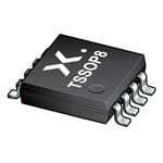
| 供应商器件封装 | 8-TSSOP |
| 其它名称 | 568-5302-1 |
| 包装 | 剪切带 (CT) |
| 封装/外壳 | 8-TSSOP,8-MSOP(0.118",3.00mm 宽) |
| 工作温度 | -40°C ~ 85°C |
| 应用 | I²C |
| 延迟时间 | - |
| 数据速率(最大值) | 1MHz |
| 标准包装 | 1 |
| 电压-电源 | 2.5 V ~ 15 V |
| 电容-输入 | 10pF |
| 电流-电源 | 5.5mA |
| 类型 | 缓冲器, 转接驱动器 |
| 输入 | 2 线式总线 |
| 输出 | 2 线式总线 |
| 通道数 | 1 |


- 商务部:美国ITC正式对集成电路等产品启动337调查
- 曝三星4nm工艺存在良率问题 高通将骁龙8 Gen1或转产台积电
- 太阳诱电将投资9.5亿元在常州建新厂生产MLCC 预计2023年完工
- 英特尔发布欧洲新工厂建设计划 深化IDM 2.0 战略
- 台积电先进制程称霸业界 有大客户加持明年业绩稳了
- 达到5530亿美元!SIA预计今年全球半导体销售额将创下新高
- 英特尔拟将自动驾驶子公司Mobileye上市 估值或超500亿美元
- 三星加码芯片和SET,合并消费电子和移动部门,撤换高东真等 CEO
- 三星电子宣布重大人事变动 还合并消费电子和移动部门
- 海关总署:前11个月进口集成电路产品价值2.52万亿元 增长14.8%


PDF Datasheet 数据手册内容提取
PCA9601 Dual bidirectional bus buffer Rev. 3 — 24 September 2015 Product data sheet 1. General description The PCA9601 is designed to isolate I2C-bus capacitance, allowing long buses to be driven in point-to-point or multipoint applications of up to 4000pF. The PCA9601 is a higher-speed version of the P82B96 and a higher drive version of the PCA9600 that allows many more Fast-mode Plus (Fm+) slaves on remote daughter cards in applications with temperature range of 0C to 85C. It creates a non-latching, bidirectional, logic interface between a normal I2C-bus and a range of other higher capacitance or different voltage bus configurations. It can operate at speeds up to at least 1MHz, and the high drive side is compatible with the Fast-mode Plus specifications. The PCA9601 features temperature-stabilized logic voltage levels at its SX/SY interface making it suitable for interfacing with buses that have non I2C-bus-compliant logic levels such as SMBus, PMBus, or with microprocessors that use those same TTL logic levels. 15mA drive capability over 0C to 85C at SX/SY allows driving a 5V Fm+ bus with 470pF loading. The separation of the bidirectional I2C-bus signals into unidirectional TX and RX signals enables the SDA and SCL signals to be transmitted via balanced transmission lines (twisted pairs), or with galvanic isolation using opto or magnetic coupling. The TX and RX signals may be connected together to provide a normal bidirectional signal. 2. Features and benefits Bidirectional data transfer of I2C-bus signals 15mA SX/SY sink capability yields 5V Fm+ bus risetime with 470pF loads Isolates capacitance allowing > 400pF on SX/SY side and 4000pF on TX/TY side 1MHz operation on up to 20meters of wire (see AN10658) Supply voltage range of 2.5V to 15V with I2C-bus logic levels on SX/SY side independent of supply voltage Splits I2C-bus signal into pairs of forward/reverse TX/RX, TY/RY signals for interface with opto-electrical isolators and similar devices that need unidirectional input and output signal paths Low power supply current ESD protection exceeds 3500V HBM per JESD22-A114, and 1400V CDM per JESD22-C101 Latch-up testing is done to JEDEC Standard JESD78 which exceeds 100mA Packages offered: SO8 and TSSOP8 (MSOP8)
PCA9601 NXP Semiconductors Dual bidirectional bus buffer 3. Applications Interface between I2C-buses operating at different logic levels (for example, 5V and 3V or 15V) Interface between I2C-bus and SMBus (350A) standard or Fm+ standard Simple conversion of I2C-bus SDA or SCL signals to multi-drop differential bus hardware, for example, via compatible PCA82C250 Interfaces with opto-couplers to provide opto-isolation between I2C-bus nodes up to 1MHz Long distance point-to-point or multipoint architectures 4. Ordering information Table 1. Ordering info rmation Type number Topside Package marking Name Description Version PCA9601D PCA9601 SO8 plastic small outline package; 8 leads; bodywidth3.9mm SOT96-1 PCA9601DP 9601 TSSOP8 plastic thin shrink small outline package; 8 leads; SOT505-1 bodywidth3mm 4.1 Ordering options Table 2. Ordering opt ions Type number Orderable Package Packing method Minimum Temperature partnumber orderquantity PCA9601D PCA9601D,118 SO8 REEL 13" Q1/T1 2500 T =40C to +85C amb *STANDARD MARK SMD PCA9601DP PCA9601DP,118 TSSOP8 REEL 13" Q1/T1 2500 T =40C to +85C amb *STANDARD MARK SMD PCA9601 All information provided in this document is subject to legal disclaimers. © NXP Semiconductors N.V. 2015. All rights reserved. Product data sheet Rev. 3 — 24 September 2015 2 of 32
PCA9601 NXP Semiconductors Dual bidirectional bus buffer 5. Block diagram VCC (2.5 V to 15 V) 8 PCA9601 1 3 SX (SDA) TX (TxD, SDA) 2 static level offset RX (RxD, SDA) higher drive, card side longer distance side 7 5 SY (SCL) TY (TxD, SCL) 6 RY (RxD, SCL) 4 GND 002aae873 Fig 1. Block diagram of PCA9601 6. Pinning information 6.1 Pinning SX 1 8 VCC SX 1 8 VCC RX 2 7 SY RX 2 7 SY PCA9601D PCA9601DP TX 3 6 RY TX 3 6 RY GND 4 5 TY GND 4 5 TY 002aae874 002aae875 Fig 2. Pin configuration for SO8 Fig 3. Pin configuration for TSSOP8 (MSOP8) 6.2 Pin description Table 3. Pin description Symbol Pin Description SX 1 I2C-bus (SDA or SCL) RX 2 receive signal TX 3 transmit signal GND 4 negative supply voltage TY 5 transmit signal RY 6 receive signal SY 7 I2C-bus (SDA or SCL) V 8 positive supply voltage CC PCA9601 All information provided in this document is subject to legal disclaimers. © NXP Semiconductors N.V. 2015. All rights reserved. Product data sheet Rev. 3 — 24 September 2015 3 of 32
PCA9601 NXP Semiconductors Dual bidirectional bus buffer 7. Functional description Refer to Figure 1 “Block diagram of PCA9601”. The PCA9601 has two identical buffers allowing buffering of SDA and SCL I2C-bus signals. Each buffer is made up of two logic signal paths, a forward path from the I2C-bus interface, pins SX and SY which drive the buffered bus, and a reverse signal path from the buffered bus input, pins RX and RY to drive the I2C-bus interface. These paths: • sense the voltage state of I2C-bus pins SX (and SY) and transmit this state to pin TX (and TY respectively), and • sense the state of pins RX and RY and pull the I2C-bus pin LOW whenever pin RX or pinRY is LOW. The rest of this discussion will address only the ‘X’ side of the buffer; the ‘Y’ side is identical. 7.1 Static level offset card side The I2C-bus pin SX is specified to allow interfacing with Fast-mode, Fm+ and TTL-based systems. The logic threshold voltage levels at SX on this I2C-bus are independent of the IC supply voltage V . The maximum I2C-bus supply voltage is 15V. CC 7.1.1 Fast-mode operation When interfacing with Fast-mode systems, the SX pin is guaranteed to sink the normal 3mA with a V of 0.74V maximum. That guarantees compliance with the Fast-mode OL I2C-bus specification for all I2C-bus voltages greater than 3V, as well as compliance with SMBus or other systems that use TTL switching levels. SX is guaranteed to sink an external 3mA in addition to its internally sourced pull-up of typically 300A (maximum 1mA at 40C). When selecting the pull-up for the bus at SX, the sink capability of other connected drivers should be taken into account. Most TTL devices are specified to sink at least 4mA so then the pull-up is limited to 3mA by the requirement to ensure the 0.8V TTL LOW. For Fast-mode I2C-bus operation, the other connected I2C-bus parts may have the minimum sink capability of 3mA. SX sources typically 300A (maximum 1mA at 40C), which forms part of the external driver loading. When selecting the pull-up it is necessary to subtract the SX pin pull-up current, so, worst-case at 40C, the allowed pull-up can be limited (by external drivers) to 2mA. 7.1.2 Fast-mode Plus operation When the interface at SX is an Fm+ bus with a voltage greater than 4V, its higher specified sink capability may be used. PCA9601 has a guaranteed sink capability of 15mA at V =1V maximum over 0C to 85C. That 1V complies with the bus LOW OL requirement (0.25V ) of any Fm+ bus operating at 4V or greater. Since the other bus connected Fm+ devices have a drive capability greater than 20mA, the pull-up may be selected for 15mA sink current at V =1V. For a nominal 5V bus (5.5V maximum) the OL allowed pull-up is (5.5V1V)/15mA=300. With 300 pull-up, the Fm+ risetime of 120ns maximum can be met with total bus loading up to 470pF. PCA9601 All information provided in this document is subject to legal disclaimers. © NXP Semiconductors N.V. 2015. All rights reserved. Product data sheet Rev. 3 — 24 September 2015 4 of 32
PCA9601 NXP Semiconductors Dual bidirectional bus buffer 7.2 High drive, long distance side The logic level on RX is determined from the power supply voltage V of the chip. Logic CC LOW is below 40% of V , and logic HIGH is above 55% of V (with a typical switching CC CC threshold just slightly below half V ). CC TX is an open-collector output without ESD protection diodes to V . It may be connected CC via a pull-up resistor to a supply voltage in excess of V , as long as the 15V rating is not CC exceeded. It has a larger current sinking capability than a normal I2C-bus device, being able to sink a static current of greater than 30mA, and typical 100mA dynamic pull-down capability as well. A logic LOW is transmitted to TX when the voltage at I2C-bus pin SX is below 0.425V. A logic LOW at RX will cause I2C-bus pin SX to be pulled to a logic LOW level in accordance with I2C-bus requirements (maximum 1.5V in 5V applications) but not low enough to be looped back to the TX output and cause the buffer to latch LOW. The LOW level this chip can achieve on the I2C-bus by a LOW at RX is typically 0.64V when sinking 1mA. If the supply voltage V fails, then neither the I2C-bus nor the TX output will be held CC LOW. Their open-collector configuration allows them to be pulled up to the rated maximum of 15V even without V present. The input configuration on SX and RX also CC presents no loading of external signals when V is not present. CC The effective input capacitance of any signal pin, measured by its effect on bus rise times, is less than 10pF for all bus voltages and supply voltages including V =0V. CC 7.3 Connections to other bus buffers Two or more SX or SY I/Os must not be interconnected. The PCA9601 design does not support this configuration. Bidirectional I2C-bus signals do not allow any direction control pin so, instead, slightly different logic LOW voltage levels are used at SX/SY to avoid latching of this buffer. A ‘regular I2C-bus LOW’ applied at the RX/RY of a PCA9601 will be propagated to SX/SY as a ‘buffered LOW’ with a slightly higher voltage level. If this special ‘buffered LOW’ is applied to the SX/SY of another PCA9601, that second PCA9601 will not recognize it as a ‘regular I2C-bus LOW’ and will not propagate it to its TX/TY output. The SX/SY side of PCA9601 may not be connected to similar buffers that rely on special logic thresholds for their operation, for example P82B96, PCA9511A, PCA9515A, ‘B’ side of PCA9517, etc. The SX/SY side is only intended for, and compatible with, the normal I2C-bus logic voltage levels of I2C-bus master and slave chips, or even TX/RX signals of a second PCA9601 or P82B96 if required. The TX/RX and TY/RY I/O pins use the standard I2C-bus logic voltage levels of all I2C-bus parts. There are no restrictions on the interconnection of the TX/RX and TY/RY I/O pins to other PCA9601s, for example in a star or multipoint configuration with the TX/RX and TY/RY I/O pins on the common bus and the SX/SY side connected to the line card slave devices. For more details see Application Note AN10658, “Sending I2C-bus signals via long communication cables”. PCA9601 All information provided in this document is subject to legal disclaimers. © NXP Semiconductors N.V. 2015. All rights reserved. Product data sheet Rev. 3 — 24 September 2015 5 of 32
PCA9601 NXP Semiconductors Dual bidirectional bus buffer 7.4 Comparison of PCA9601/PCA9600 and P82B96 The PCA9601 is a direct upgrade of the P82B96 with the significant differences summarized in Table4. The PCA9601 provides improved interface to the higher drive Fast-mode Plus devices on the SX/SY sides. Table 4. PCA9601/PC A9600 versus P82B96 Detail PCA9601/PCA9600 P82B96 Supply voltage (V ) range: 2.5V to 15V 2V to 15V CC Maximum operating bus voltage 15V 15V (independent of V ): CC Typical operating supply current: 5mA 1mA Typical LOW-level input voltage on I2C-bus 0.5V over 40C to +85C 0.65V at 25C (SX/SYside): LOW-level output voltage on I2C-bus 0.74V (max.) over 40C to +85C 0.88V (typ.) at 25C (SX/SYside;3mAsink): LOW-level output voltage on Fm+ I2C-bus 1V (max.) over 0C to 85C n/a (SX/SY side; 15mA sink): (PCA9601 only) Temperature coefficient of V /V : 0mV/C 2mV/C IL OL Logic voltage levels on SX/SY bus compatible with I2C-bus and similar compatible with I2C-bus and similar (independentof V ): buses using TTL levels (SMBus, etc.) buses using TTL levels (SMBus, etc.) CC Typical propagation delays: <100ns <200ns TX/RX switching specifications (I2C-bus yes, all classes including 1MHz Fm+ yes, all classes including Fm+ compliant): RX logic levels with tighter control than yes, 40% to 55% (48% nominal) yes, 42% to 58% (50% nominal) I2C-bus limit of 30% to 70%: Maximum bus speed: >1MHz >400kHz ESD rating HBM per JESD22-A114: >3500V >3500V Package: SO8, TSSOP8 (MSOP8) SO8, TSSOP8 (MSOP8) When the device driving the PCA9601/PCA9600 is an I2C-bus compatible device, then the PCA9601 is an improvement on the P82B96 as shown in Table4. There will always be exceptions however, and if the device driving the bus buffer is not I2C-bus compatible (e.g., you need to use the micro already in the system and bit-bang using two GPIO pins) then here are some considerations that would point to using the P82B96 instead: • When the pull-up must be the weakest one possible. The spec is 200 A for P82B96, but it typically works even below that. And if designing for a temperature range 40C up to +60C, then the driver when sinking 200A only needs to drive a guaranteed low of 0.55V. For the PCA9601/PCA9600, over that same temperature range and when sinking 1.3mA (at40C), the device driving the bus buffer must provide the required low of 0.425V. • When the lower operating temperature range is restricted (say 0C). The P82B96 larger SX voltage levels then make a better typical match with the driver, even when the supply is as low as 3.3V. For an I2C-bus compliant driver on 3.3V the P82B96 is required to guarantee a bus low that is below 0.83V. P82B96 guarantees that with a 200A pull-up. PCA9601 All information provided in this document is subject to legal disclaimers. © NXP Semiconductors N.V. 2015. All rights reserved. Product data sheet Rev. 3 — 24 September 2015 6 of 32
PCA9601 NXP Semiconductors Dual bidirectional bus buffer • When the operating temperature range is restricted at both limits. An I2C driver's typical output is well below 0.4V and the P82B96 typically requires 0.6V input even at +60C, so there is a reasonable margin. The PCA9601/PCA9600 requires a typical input low of 0.5V so its typical margin is smaller. At 0C the driver requires a typical input low of 1.16V and P82B96 provides 0.75V, so again the typical margin is already quite big and even though PCA9601/PCA9600 is better, providing 0.7V, that difference is not big. 8. Limiting values Table 5. Limiting values In accordance with the Absolute Maximum Rating System (IEC 60134). Voltages with respect to pin GND. Symbol Parameter Conditions Min Max Unit V supply voltage V to GND 0.3 +18 V CC CC V I2C-bus voltage SX and SY; 0.3 +18 V I2C-bus I2C-busSDA or SCL V output voltage TX and TY; [1] 0.3 +18 V O bufferedoutput V input voltage RX and RY; [1] 0.3 +18 V I receiveinput I I2C-bus current SX and SY; - 250 mA I2C-bus I2C-busSDA or SCL P total power dissipation - 300 mW tot T junction temperature operating range 40 +125 C j T storage temperature 55 +125 C stg T ambient temperature operating 40 +85 C amb [1] See also Section 10.2 “Negative undershoot below absolute minimum value”. PCA9601 All information provided in this document is subject to legal disclaimers. © NXP Semiconductors N.V. 2015. All rights reserved. Product data sheet Rev. 3 — 24 September 2015 7 of 32
PCA9601 NXP Semiconductors Dual bidirectional bus buffer 9. Characteristics Table 6. Characterist ics T =40C to +85C unless otherwise specified; voltages are specified with respect to GND with V =2.5V to 15V amb CC unless otherwise specified. Typical values are measured at V =5V and T =25C. CC amb Symbol Parameter Conditions Min Typ Max Unit Power supply V supply voltage operating 2.5 - 15 V CC I supply current V =5V; buses HIGH - 5.2 6.75 mA CC CC V =15V; buses HIGH - 5.5 7.3 mA CC I additional supply current per TX/TY output driven LOW; - 1.4 3.0 mA CC V =5.5V CC Bus pull-up (load) voltages and currents Pins SX and SY; I2C-bus V input voltage open-collector; RXand RYHIGH - - 15 V I V output voltage open-collector; RXand RYHIGH - - 15 V O I output current static; V = V = 0.4V [1] 0.3 - 15 mA O SX SY I output sink current V = V = 1V; RXandRYLOW; 15 - - mA O(sink) SX SY T =0Cto85C amb I leakage current V = V = 15V; RX and RY HIGH - - 10 A L SX SY Pins TX and TY V output voltage open-collector - - 15 V O I load current maximum recommended on - - 30 mA load buffered bus; V =V =0.4V; TX TY SXand SY LOW on I2C-bus=0.4V I output current from buffered bus; V =V =1V; 60 130 - mA O TX TY SX and SY LOW on I2C-bus=0.4V I leakage current on buffered bus; - - 10 A L V =V =V =15V; SX and TX TY CC SYHIGH Input currents I input current from I2C-bus on SX and SY I RX and RY HIGHorLOW; [1] - 0.3 1 mA SXand SY LOW1V RX and RYHIGH; SX and [1] - - 10 A SYHIGH>1.4V from buffered bus on RX and RY; [2] - 1.5 10 A SX and SY HIGHorLOW; V =V =0.4V RX RY I leakage current on bufferedbus input on RX and - - 10 A L RY; V = V =15V RX RY PCA9601 All information provided in this document is subject to legal disclaimers. © NXP Semiconductors N.V. 2015. All rights reserved. Product data sheet Rev. 3 — 24 September 2015 8 of 32
PCA9601 NXP Semiconductors Dual bidirectional bus buffer Table 6. Characteristics …continued T =40C to +85C unless otherwise specified; voltages are specified with respect to GND with V =2.5V to 15V amb CC unless otherwise specified. Typical values are measured at V =5V and T =25C. CC amb Symbol Parameter Conditions Min Typ Max Unit Output logic LOW level Pins SX and SY V LOW-level output voltage on Standard-mode or Fast-mode OL I2C-bus I =I = 3mA; Figure6 - 0.7 0.74 V SX SY I =I = 0.3mA; Figure5 - 0.6 0.65 V SX SY on 5V Fm+ I2C-bus I =I = 15mA; - 0.85 1 V SX SY T =0Cto85C amb V/T voltage variation with I =I = 0.3mAto3mA - 0 - %/K SX SY temperature Input logic switching threshold voltages Pins SX and SY V LOW-level input voltage on normal I2C-bus; Figure7 [3] - - 425 mV IL V HIGH-level input threshold on normal I2C-bus; Figure8 580 - - mV th(IH) voltage V/T voltage variation with - 0 - %/K temperature Pins RX and RY V HIGH-level input voltage fraction of applied V 0.55V - - V IH CC CC V input threshold voltage fraction of applied V - 0.48V - V th(i) CC CC V LOW-level input voltage fraction of applied V - - 0.4V V IL CC CC Logic level threshold difference V voltage difference SX and SY; SX output LOW at [4] 50 - - mV 0.3mAtoSX input HIGH maximum Bus release on V failure CC V supply voltage SX, SY, TX and TY; voltage at which - - 1 V CC all buses are to be released at 25C V/T voltage variation with Figure9 - 4 - %/K temperature PCA9601 All information provided in this document is subject to legal disclaimers. © NXP Semiconductors N.V. 2015. All rights reserved. Product data sheet Rev. 3 — 24 September 2015 9 of 32
PCA9601 NXP Semiconductors Dual bidirectional bus buffer Table 6. Characteristics …continued T =40C to +85C unless otherwise specified; voltages are specified with respect to GND with V =2.5V to 15V amb CC unless otherwise specified. Typical values are measured at V =5V and T =25C. CC amb Symbol Parameter Conditions Min Typ Max Unit Buffer response time[5] V = 5 V; pin TX pull-up resistor=160; pin SX pull-up resistor=2.2k; nocapacitive load CC t delay time V to V , V to V ; on falling - 50 - ns d SX TX SY TY input between V =input switching SX threshold, and V output falling to TX 50% V CC V to V , V to V ; on rising - 60 - ns SX TX SY TY input between V =input switching SX threshold, and V output reaching TX 50% V CC V to V , V to V ; on falling - 100 - ns RX SX RY SY input between V =input switching RX threshold, and V output falling to SX 50% V CC V to V , V to V ; on rising - 95 - ns RX SX RY SY input between V =input switching RX threshold, and V output reaching SX 50% V CC Input capacitance C input capacitance effective input capacitance of any - - 10 pF i signal pin measured by incremental bus rise times; guaranteed by design, not production tested [1] This bus pull-up current specification is intended to assist design of the bus pull-up resistor. It is not a specification of the sink capability (see VOL under sub-section “Output logic LOW level”). When used on an Fm+ bus the load current is limited to 15mA by the drive capability of PCA9601. When used in a standard I2C-bus the load current is limited by the drive capability of other devices on the bus. The maximum static sink current for a Standard/Fast-mode I2C-bus is 3mA and PCA9601 is guaranteed to sink more than 3mA at SX/SY when its pins are holding the bus LOW. However, when an external device pulls the SX/SY pins below 1.4V, the PCA9601 will source a current between 0mA and 1mA maximum. When that other external device is driving LOW it will pull the bus connected to SX or SY down to, or below, the 0.4V level referenced in the I2C-bus specification and in these test conditions. Then that device must be able to sink up to 1mA coming from SX/SY plus the usual pull-up current. Therefore in Standard and Fast-mode systems the external pull-up used at SX/SY should be limited to 2mA. The typical and maximum currents sourced by SX/SY as a function of junction temperature are shown in Figure10, and the equivalent circuit at the SX/SY interface is shown in Figure4. [2] Valid over temperature for VCC5V. At higher VCC, this current may increase to maximum 20A at VCC=15V. [3] The input logic threshold is independent of the supply voltage. [4] The minimum value requirement for pull-up current, 0.3mA, guarantees that the minimum value for V output LOW will always exceed SX the maximum VSX input HIGH level to eliminate any possibility of latching. The specified difference is guaranteed by design within any IC. While the tolerances on absolute levels allow a small probability, the LOW from one SX output is recognized by an SX input of another PCA9601, this has no consequences for normal applications. In any design the SX pins of different ICs should never be linked because the resulting system would be very susceptible to induced noise and would not support all I2C-bus operating modes. [5] The fall time of V from 5V to 2.5V in the test is approximately 10ns. TX The fall time of V from 5V to 2.5V in the test is approximately 20ns. SX The rise time of V from 0V to 2.5V in the test is approximately 15ns. TX The rise time of V from 0.7V to 2.5V in the test is approximately 25ns. SX PCA9601 All information provided in this document is subject to legal disclaimers. © NXP Semiconductors N.V. 2015. All rights reserved. Product data sheet Rev. 3 — 24 September 2015 10 of 32
PCA9601 NXP Semiconductors Dual bidirectional bus buffer VCC ≤ 1 mA SX (SY) Vref 002aac838 Fig 4. Equivalent circuit at SX/SY 002aac839 002aac840 800 800 VOL VOL (1) (mV) (mV) (2) 700 700 (1) (2) 600 600 500 500 400 400 −50 −25 0 25 50 75 100 125 −50 −25 0 25 50 75 100 125 Tj (°C) Tj (°C) V at SX typical and limits over temperature. V at SX typical and limits over temperature. OL OL (1) Maximum. (1) Maximum. (2) Typical. (2) Typical. Fig 5. V as a function of junction temperature Fig 6. V as a function of junction temperature OL OL (I =0.3mA) (I =3mA) OL OL 600 002aag005 600 002aag006 VIL VIH minimum (mV) (mV) typical 500 500 typical maximum 400 400 300 300 200 200 −50 −25 0 25 50 75 100 125 −50 −25 0 25 50 75 100 125 Tj (°C) Tj (°C) V at SX changes over temperature range. V at SX changes over temperature range. IL IH Fig 7. V as a function of junction temperature; Fig 8. V as a function of junction temperature; IL IH maximum and typical values minimum and typical values PCA9601 All information provided in this document is subject to legal disclaimers. © NXP Semiconductors N.V. 2015. All rights reserved. Product data sheet Rev. 3 — 24 September 2015 11 of 32
PCA9601 NXP Semiconductors Dual bidirectional bus buffer 1400 002aac075 1000 001aai062 VCC(max) II (mV) (μA) (1) 1200 800 (2) 1000 600 800 400 600 200 400 0 −50 −25 0 25 50 75 100 125 −50 −25 0 25 50 75 100 125 Tj (°C) Tj (°C) (1) Maximum. (2) Typical. Fig 9. V bus release limit over temperature; Fig 10. Current sourced out of SX/SY as a function of CC maximum values junction temperature if these pins are externally pulled to 0.4V or lower 002aaf484 1.4 VOL (V) 1.2 1.0 0.8 0.6 0.4 0.2 0 0 10 20 30 ISX, ISY (mA) Fig 11. Typical SX/SY current versus LOW-level output voltage PCA9601 All information provided in this document is subject to legal disclaimers. © NXP Semiconductors N.V. 2015. All rights reserved. Product data sheet Rev. 3 — 24 September 2015 12 of 32
PCA9601 NXP Semiconductors Dual bidirectional bus buffer 10. Application information Refer to application notes AN10658 and AN255 for more detailed application information. VCC (2.5 V to 15 V) 5 V TX R1 I2C-bus (SDA) SDA 'SDA' (new levels) RX (SDA) PCA9601 002aae876 Fig 12. Interfacing a standard 3mA I2C-bus or one with TTL levels (e.g. SMBus) to highervoltage or higher current sink (e.g. Fast-mode Plus) devices VCC VCC1 R2 R4 R5 RX R3 I2C-bus 5 V (SDA) SDA R1 TX I2C-bus (SDA) SDA PCA9601 002aae877 This simple example may be limited, if using lowest-cost couplers, to speeds as low as 5kHz. Refer to application notes for schematics suitable for operation to 400kHz or higher. Fig 13. Galvanic isolation of I2C-bus nodes via opto-couplers main enclosure remote control enclosure 3.3 V to 5 V 12 V 12 V 3.3 V to 5 V long cables SDA SDA 3.3 V to 5 V 12 V 3.3 V to 5 V SCL SCL PCA9601 PCA9601 002aae878 Fig 14. Long distance I2C-bus communication PCA9601 All information provided in this document is subject to legal disclaimers. © NXP Semiconductors N.V. 2015. All rights reserved. Product data sheet Rev. 3 — 24 September 2015 13 of 32
PCA9601 NXP Semiconductors Dual bidirectional bus buffer +V cable drive VCC1 VCC2 R2 R2 VCC VCC R2 RX R1 R1 R1 R1 RX R2 SCL SX TX TX SX SCL I2C-BUS TY TY I2C-BUS MASTER SLAVE(S) SDA SY RY RY SY SDA cable PCA9601 PCA9601 propagation C2 C2 delay ≈ 5 ns/m C2 C2 GND GND BAT54A BAT54A 002aae879 Fig 15. Driving ribbon or flat telephone cables Table 7. Examples of bus capability Refer to Figure15. V +V V R1 R2 C2 Cable Cable Cable Set master Effective Max. slave CC1 CC2 (V) cable (V) () (k) (pF) length capacitance delay nominal SCL bus response (V) (m) clock delay HIGH LOW speed period period (kHz) (ns) (ns) 5 12 5 750 2.2 400 250 n/a 1.25s 600 3850 125 normal (delaybased) specification 400kHz parts 5 12 5 750 2.2 220 100 n/a 500ns 600 2450 195 normal (delaybased) specification 400kHz parts 3.3 5 3.3 330 1 220 25 1nF 125ns 260 770 620 meets Fm+ specification 3.3 5 3.3 330 1 100 3 120pF 15ns 260 720 690 meets Fm+ specification For more examples of faster alternatives for driving over longer cables such as Cat5 communication cable, see AN10658. Communication at 1MHz is possible over short cables and >400kHz is possible over 50m of cable. PCA9601 All information provided in this document is subject to legal disclaimers. © NXP Semiconductors N.V. 2015. All rights reserved. Product data sheet Rev. 3 — 24 September 2015 14 of 32
PCA9601 NXP Semiconductors Dual bidirectional bus buffer 10.1 Calculating system delays and bus clock frequency local master bus buffered expansion bus remote slave bus VCCM VCCB VCCS Rm Rb Rs SCL SCL MASTER SLAVE SX TX/RX TX/RX SX PCA9601 PCA9601 I2C-BUS I2C-BUS Cm Cb Cs master bus buffered bus slave bus capacitance wiring capacitance capacitance GND (0 V) 002aae880 Effective delay of SCL at slave: 120+17VCCM+(2.5+4109Cb)VCCB+10VCCS (ns). C=F; V=V. Fig 16. Falling edge of SCL at master is delayed by the buffers and bus fall times local master bus buffered expansion bus VCCM VCCB Rm Rb SCL MASTER SX TX/RX PCA9601 TX/RX I2C-BUS Cm Cb master bus buffered bus capacitance wiring capacitance GND (0 V) 002aae881 Effective delay of SCL at master: 115+(RmCm)+(0.7RbCb) (ns). C=F; R=. Fig 17. Rising edge of SCL at master is delayed (clock stretch) by buffer and bus rise times PCA9601 All information provided in this document is subject to legal disclaimers. © NXP Semiconductors N.V. 2015. All rights reserved. Product data sheet Rev. 3 — 24 September 2015 15 of 32
PCA9601 NXP Semiconductors Dual bidirectional bus buffer local master bus buffered expansion bus remote slave bus VCCM VCCB VCCS Rm Rb Rs SDA SDA MASTER SLAVE SX TX/RX TX/RX SX PCA9601 PCA9601 I2C-BUS I2C-BUS Cm Cb Cs master bus buffered bus slave bus capacitance wiring capacitance capacitance GND (0 V) 002aae882 Effective delay of SDA at master: 115+0.2(RsCs)+0.7[(RbCb)+(RmCm)] (ns). C=F; R=. Fig 18. Rising edge of SDA at slave is delayed by the buffers and bus rise times Figure16, Figure17, and Figure18 show the PCA9601 used to drive extended bus wiring with relatively large capacitances linking two I2C-bus nodes. It includes simplified expressions for making the relevant timing calculations for 3.3V or 5V operation. Because the buffers and the wiring introduce timing delays, it may be necessary to decrease the nominal SCL frequency. In most cases the actual bus frequency will be lower than the nominal Master timing due to bit-wise stretching of the clock periods. The delay factors involved in calculation of the allowed bus speed are: A — The propagation delay of the master signal through the buffers and wiring to the slave. The important delay is that of the falling edge of SCL because this edge ‘requests’ the data or acknowledge from a slave. See Figure16. B — The effective stretching of the nominal LOW period of SCL at the master caused by the buffer and bus rise times. See Figure17. C — The propagation delay of the slave's response signal through the buffers and wiring back to the master. The important delay is that of a rising edge in the SDA signal. Rising edges are always slower and are therefore delayed by a longer time than falling edges. (The rising edges are limited by the passive pull-up while falling edges are actively driven); see Figure18. The timing requirement in any I2C-bus system is that a slave's data response (which is provided in response to a falling edge of SCL) must be received at the master before the end of the corresponding LOW period of SCL as appears on the bus wiring at the master. Since all slaves will, as a minimum, satisfy the worst case timing requirements of their speed class (Fast-mode, Fm+, etc.), they must provide their response, allowing for the set-up time, within the minimum allowed clock LOW period, e.g., 450ns (max.) for Fm+ parts. In systems that introduce additional delays it may be necessary to extend the minimum clock LOW period to accommodate the ‘effective’ delay of the slave's response. The effective delay of the slave’s response equals the total delays in SCL falling edge from the master reaching the slave (Figure16) minus the effective delay (stretch) of the SCL rising edge (Figure17) plus total delays in the slave's response data, carried on PCA9601 All information provided in this document is subject to legal disclaimers. © NXP Semiconductors N.V. 2015. All rights reserved. Product data sheet Rev. 3 — 24 September 2015 16 of 32
PCA9601 NXP Semiconductors Dual bidirectional bus buffer SDA, reaching the master (Figure18). The master microcontroller should be programmed to produce a nominal SCL LOW period as follows: SCL LOWslave response delay to valid data on its SDA+A–B+C+data set-up time ns (1) The actual LOW period will become (the programmed value+the stretching time B). When this actual LOW period is then less than the specified minimum, the specified minimum should be used. Example 1: It is required to connect an Fm+ slave, with RsCs product of 100ns, to a 5V Fast-mode system also having 100ns RmCm using twoPCA9601’s to buffer a 5V bus with 4nF loading and 160 pull-up. Calculate the allowed bus speed: Delay A = 120 + 85 + (2.5 + [44]) 5 + 50=347.5ns Delay B = 115 + 100 + 70=285ns Delay C = 115 + 20 + 0.7(100 + 100)=275ns The maximum Fm+ slave response delay must be <450ns so the programmed LOW period is calculated as: LOW450 + 347.5 285 + 275 + 100=887.5ns The actual LOW period will be 887.5 + 285=1173 ns, which is below the Fast-mode minimum, so the programmed LOW period must be increased to (1300285)=1015ns, so the actual LOW equals the 1300ns requirement and this shows that this Fast-mode system may be safely run to its limit of 400kHz. Example 2: It is required to buffer a Master with Fm+ speed capability, but only 3mA sink capability, to an Fm+ bus. All the system operates at 3.3V. The Master RmCm product is 50ns. Only one PCA9601 is used. The Fm+ bus becomes the buffered bus. The Fm+ bus has 200pF loading and 150 pull-up, so its RbCb product is 30ns. The Fm+ slave has a specified data valid time t maximum of 300ns. VD;DAT Calculate the allowed maximum system bus speed. (Note that the fixed values in the delay equations represent the internal propagation delays of the PCA9601. Only one PCA9601 is used here, so those fixed values used below are taken from the characteristics.) The delays are: Delay A = 40 + 56 + (2.5 + [40.2]) 3.3 = 107ns Delay B = 115 + 50 + 21 = 186ns Delay C = 70 + 0.7(50 + 30) = 126ns The programmed LOW period is calculated as: SCL LOW 300 + 117 186 + 126 + 50 = 407ns The actual LOW period will be 407 + 126 = 533ns, which exceeds the minimum Fm+ 500ns requirement. This system requires the bus LOW period, and therefore cycle time, to be increased by 33ns so the system must run slightly below the 1MHz limit. PCA9601 All information provided in this document is subject to legal disclaimers. © NXP Semiconductors N.V. 2015. All rights reserved. Product data sheet Rev. 3 — 24 September 2015 17 of 32
PCA9601 NXP Semiconductors Dual bidirectional bus buffer The possible maximum speed has a cycle period of 1033ns or 968kHz. 12 V 12 V twisted-pair telephone wires, 3.3 V to 5 V USB, or flat ribbon cables; up to 15 V logic levels, TX include VCC and GND SX SDA RX 3.3 V to 5 V 12 V TY 3.3 V 3.3 V SY SCL RY PCA9601 PCA9601 PCA9601 PCA9601 PCA9601 SX SY SX SY SX SY SY SDA SCL/SDA SCL/SDA SCL/SDA SX SCL no limit to the number of connected bus devices 002aae883 Fig 19. I2C-bus multipoint application There is an Excel calculator which makes it easy to determine the maximum I2C-bus clock speed when using the PCA9601. The calculator and instructions can be found at www.nxp.com/clockspeedcalculator. PCA9601 All information provided in this document is subject to legal disclaimers. © NXP Semiconductors N.V. 2015. All rights reserved. Product data sheet Rev. 3 — 24 September 2015 18 of 32
PCA9601 NXP Semiconductors Dual bidirectional bus buffer 002aac932 002aac933 7 7 VCC 6 VCC 6 (V) (V) (1) (1) 5 5 4 4 3 3 (2) (2) 2 2 1 1 (1) (2) (1) 0 0 (2) (2) −1 −1 0 100 200 300 400 500 600 700 800 900 0 100 200 300 400 500 600 700 800 900 time (ns) time (ns) (1) TX output. (1) TX/RX output. (2) SX input. (2) SX input. Fig 20. Propagation SX to TX with V =V =3.3V Fig 21. Propagation SX to TX with RX tied to TX; RX CC (SXpull-up to 3.3V; TXpull-up to 5.7V) V =3.3V (SXpull-up to 3.3V; TXpull-up to CC 5.7V) 002aac934 7 VCC 6 (V) 5 4 (1) 3 (2) 2 (2) 1 0 (1) −1 0 100 200 300 400 500 600 700 800 900 time (ns) (1) RX input. (2) SX output. Fig 22. Propagation RX to SX (SXpull-up to 3.3V; V =3.3V; RXpull-up to 4.6V) CC 10.2 Negative undershoot below absolute minimum value The reason why the IC pin reverse voltage on pins TX and RX in Table 5 “Limiting values” is specified at such a low value, 0.3V, is not that applying larger voltages is likely to cause damage but that it is expected that, in normal applications, there is no reason why larger DC voltages will be applied. This ‘absolute maximum’ specification is intended to be a DC or continuous ratings and the nominal DC I2C-bus voltage LOW usually does not even reach 0V. Inside PCA9601 at every pin there is a large protective diode connected to the GND pin and that diode will start to conduct when the pin voltage is more than about 0.55V with respect to GND at 25C ambient. Figure23 shows the measured characteristic for one of those diodes inside PCA9601. The plot was made using a curve tracer that applies 50Hz mains voltage via a series resistor, so the pulse durations are long duration (several milliseconds) and are reaching peaks of over 2A when more than 1.5V is applied. The IC becomes very hot during this PCA9601 All information provided in this document is subject to legal disclaimers. © NXP Semiconductors N.V. 2015. All rights reserved. Product data sheet Rev. 3 — 24 September 2015 19 of 32
PCA9601 NXP Semiconductors Dual bidirectional bus buffer testing but it was not damaged. Whenever there is current flowing in any of these diodes it is possible that there can be faulty operation of any IC. For that reason we put a specification on the negative voltage that is allowed to be applied. It is selected so that, at the highest allowed junction temperature, there will be a big safety factor that guarantees the diode will not conduct and then we do not need to make any 100% production tests to guarantee the published specification. For the PCA9601, in specific applications, there will always be transient overshoot and ringing on the wiring that can cause these diodes to conduct. Therefore we designed the IC to withstand those transients and as a part of the qualification procedure we made tests, using DC currents to more than twice the normal bus sink currents, to be sure that the IC was not affected by those currents. For example, the TX/TY and RX/RY pins were tested to at least 80mA which, from Figure23, would be more than 0.8V. The correct functioning of the PCA9601 is not affected even by those large currents. The Absolute Maximum (DC) ratings are not intended to apply to transients but to steady state conditions. This explains why you will never see any problems in practice even if, during transients, more than 0.3V is applied to the bus interface pins of PCA9601. Figure 23 “Diode characteristic curve” also explains how the general Absolute Maximum DC specification was selected. The current at 25C is near zero at 0.55V. The PCA9601 is allowed to operate with +125C junction and that would cause this diode voltage to decrease by 1002mV=200mV. So for zero current we need to specify 0.35V and we publish 0.3V just to have some extra margin. Remark: You should not be concerned about the transients generated on the wiring by a PCA9601 in normal applications and that is input to the TX/RX or TY/RY pins of another PCA9601. Because not all ICs that may be driven by PCA9601 are designed to tolerate negative transients, in Section 10.2.1 “Example with questions and answers” we show they can be managed if required. 002aaf063 0 diode current (mA) −10−1 −1 −10 −102 −103 −104 −2.0 −1.5 −1.0 −0.5 0 voltage (V) Fig 23. Diode characteristic curve PCA9601 All information provided in this document is subject to legal disclaimers. © NXP Semiconductors N.V. 2015. All rights reserved. Product data sheet Rev. 3 — 24 September 2015 20 of 32
PCA9601 NXP Semiconductors Dual bidirectional bus buffer 10.2.1 Example with questions and answers Question: On a falling edge of TX we measure undershoot at 800mV at the linked TX, RX pins of the PCA9601 that is generating the LOW, but the PCA9601 datasheet specifies minimum 0.3V. Does this mean that we violate the datasheet absolute value? Answer: For PCA9601 the 0.3V Absolute Maximum rating is not intended to apply to transients, it is a DC rating. As shown in Figure24, there is no theoretical reason for any undershoot at the IC that is driving the bus LOW and no significant undershoot should be observed when using reasonable care with the ground connection of the ‘scope. It is more likely that undershoot observed at a driving PCA9601 is caused by local stray inductance and capacitance in the circuit and by the oscilloscope connections. As shown, undershoot will be generated by PCB traces, wiring, or cables driven by a PCA9601 because the allowed value of the I2C-bus pull-up resistor generally is larger than that required to correctly terminate the wiring. In this example, with no IC connected at the end of the wiring, the undershoot is about 2V. 6 voltage (V) 4 send 2 receive 0 −2 horizontal scale = 62.5 ns/div time (ns) 5 V 5 V 5 V 300 Ω 300 Ω RX SX TX send receive 2 meter PCA9601 cable GND 002aaf078 Fig 24. Transients generated by the bus wiring PCA9601 All information provided in this document is subject to legal disclaimers. © NXP Semiconductors N.V. 2015. All rights reserved. Product data sheet Rev. 3 — 24 September 2015 21 of 32
PCA9601 NXP Semiconductors Dual bidirectional bus buffer Question: We have 2 meters of cable in a bus that joins the TX/RX sides of two PCA9601 devices. When one TX drives LOW the other PCA9601 TX/RX is driven to 0.8V for over 50ns. What is the expected value and the theoretically allowed value of undershoot? Answer: Because the cable joining the two PCA9601s is a ‘transmission line’ that will have a characteristic impedance around 100 and it will be terminated by pull-up resistors that are larger than that characteristic impedance there will always be negative undershoot generated. The duration of the undershoot is a function of the cable length and the input impedance of the connected IC. As shown in Figure25, the transient undershoot will be limited, by the diodes inside PCA9601, to around 0.8V and that will not cause problems for PCA9601. Those transients will not be passed inside the IC to the SX/SY side of the IC. 6 voltage (V) 4 2 send receive 0 −2 horizontal scale = 62.5 ns/div time (ns) 5 V 5 V 5 V 5 V 300 Ω 300 Ω RX RX SX SX TX send receive TX 2 meter PCA9601 cable GND 002aaf079 Fig 25. Wiring transients limited by the diodes in PCA9601 Question: If we input 800mV undershoot at TX, RX pins, what kind of problem is expected? Answer: When that undershoot is generated by another PCA9601 and is simply the result of the system wiring, then there will be no problems. Question: Will we have any functional problem or reliability problem? Answer: No. PCA9601 All information provided in this document is subject to legal disclaimers. © NXP Semiconductors N.V. 2015. All rights reserved. Product data sheet Rev. 3 — 24 September 2015 22 of 32
PCA9601 NXP Semiconductors Dual bidirectional bus buffer Question: If we add 100 to 200 at signal line, the overshoot becomes slightly smaller. Is this a good idea? Answer: No, it is not necessary to add any resistance. When the logic signal generated by TX or TY of PCA9601 drives long traces or wiring with ICs other than PCA9601 being driven, then adding a Schottky diode (BAT54A) as shown in Figure26 will clamp the wiring undershoot to a value that will not cause conduction of the IC’s internal diodes. 6 voltage (V) 4 2 send 0 receive −2 horizontal scale = 62.5 ns/div time (ns) 5 V 5 V 5 V 5 V 300 Ω 300 Ω RX RX SX SX TX send receive TX 2 meter PCA9601 cable 1/2 BAT54A GND 002aaf080 Fig 26. Wiring transients limited by a Schottky diode PCA9601 All information provided in this document is subject to legal disclaimers. © NXP Semiconductors N.V. 2015. All rights reserved. Product data sheet Rev. 3 — 24 September 2015 23 of 32
PCA9601 NXP Semiconductors Dual bidirectional bus buffer 11. Package outline SO8: plastic small outline package; 8 leads; body width 3.9 mm SOT96-1 D E A X c y HE v M A Z 8 5 Q A2 A1 (A 3 ) A pin 1 index θ Lp 1 4 L e w M detail X bp 0 2.5 5 mm scale DIMENSIONS (inch dimensions are derived from the original mm dimensions) UNIT mAax. A1 A2 A3 bp c D(1) E(2) e HE L Lp Q v w y Z(1) θ 0.25 1.45 0.49 0.25 5.0 4.0 6.2 1.0 0.7 0.7 mm 1.75 0.25 1.27 1.05 0.25 0.25 0.1 0.10 1.25 0.36 0.19 4.8 3.8 5.8 0.4 0.6 0.3 8o 0.010 0.057 0.019 0.0100 0.20 0.16 0.244 0.039 0.028 0.028 0o inches 0.069 0.01 0.05 0.041 0.01 0.01 0.004 0.004 0.049 0.014 0.0075 0.19 0.15 0.228 0.016 0.024 0.012 Notes 1. Plastic or metal protrusions of 0.15 mm (0.006 inch) maximum per side are not included. 2. Plastic or metal protrusions of 0.25 mm (0.01 inch) maximum per side are not included. OUTLINE REFERENCES EUROPEAN ISSUE DATE VERSION IEC JEDEC JEITA PROJECTION 99-12-27 SOT96-1 076E03 MS-012 03-02-18 Fig 27. Package outline SOT96-1 (SO8) PCA9601 All information provided in this document is subject to legal disclaimers. © NXP Semiconductors N.V. 2015. All rights reserved. Product data sheet Rev. 3 — 24 September 2015 24 of 32
PCA9601 NXP Semiconductors Dual bidirectional bus buffer TSSOP8: plastic thin shrink small outline package; 8 leads; body width 3 mm SOT505-1 D E A X c y HE v M A Z 8 5 A2 A1 (A3) A pin 1 index θ Lp L 1 4 detail X e w M bp 0 2.5 5 mm scale DIMENSIONS (mm are the original dimensions) UNIT mAax. A1 A2 A3 bp c D(1) E(2) e HE L Lp v w y Z(1) θ mm 1.1 0.15 0.95 0.25 0.45 0.28 3.1 3.1 0.65 5.1 0.94 0.7 0.1 0.1 0.1 0.70 6° 0.05 0.80 0.25 0.15 2.9 2.9 4.7 0.4 0.35 0° Notes 1. Plastic or metal protrusions of 0.15 mm maximum per side are not included. 2. Plastic or metal protrusions of 0.25 mm maximum per side are not included. OUTLINE REFERENCES EUROPEAN ISSUE DATE VERSION IEC JEDEC JEITA PROJECTION 99-04-09 SOT505-1 03-02-18 Fig 28. Package outline SOT505-1 (TSSOP8) PCA9601 All information provided in this document is subject to legal disclaimers. © NXP Semiconductors N.V. 2015. All rights reserved. Product data sheet Rev. 3 — 24 September 2015 25 of 32
PCA9601 NXP Semiconductors Dual bidirectional bus buffer 12. Soldering of SMD packages This text provides a very brief insight into a complex technology. A more in-depth account of soldering ICs can be found in Application Note AN10365 “Surface mount reflow soldering description”. 12.1 Introduction to soldering Soldering is one of the most common methods through which packages are attached to Printed Circuit Boards (PCBs), to form electrical circuits. The soldered joint provides both the mechanical and the electrical connection. There is no single soldering method that is ideal for all IC packages. Wave soldering is often preferred when through-hole and Surface Mount Devices (SMDs) are mixed on one printed wiring board; however, it is not suitable for fine pitch SMDs. Reflow soldering is ideal for the small pitches and high densities that come with increased miniaturization. 12.2 Wave and reflow soldering Wave soldering is a joining technology in which the joints are made by solder coming from a standing wave of liquid solder. The wave soldering process is suitable for the following: • Through-hole components • Leaded or leadless SMDs, which are glued to the surface of the printed circuit board Not all SMDs can be wave soldered. Packages with solder balls, and some leadless packages which have solder lands underneath the body, cannot be wave soldered. Also, leaded SMDs with leads having a pitch smaller than ~0.6mm cannot be wave soldered, due to an increased probability of bridging. The reflow soldering process involves applying solder paste to a board, followed by component placement and exposure to a temperature profile. Leaded packages, packages with solder balls, and leadless packages are all reflow solderable. Key characteristics in both wave and reflow soldering are: • Board specifications, including the board finish, solder masks and vias • Package footprints, including solder thieves and orientation • The moisture sensitivity level of the packages • Package placement • Inspection and repair • Lead-free soldering versus SnPb soldering 12.3 Wave soldering Key characteristics in wave soldering are: • Process issues, such as application of adhesive and flux, clinching of leads, board transport, the solder wave parameters, and the time during which components are exposed to the wave • Solder bath specifications, including temperature and impurities PCA9601 All information provided in this document is subject to legal disclaimers. © NXP Semiconductors N.V. 2015. All rights reserved. Product data sheet Rev. 3 — 24 September 2015 26 of 32
PCA9601 NXP Semiconductors Dual bidirectional bus buffer 12.4 Reflow soldering Key characteristics in reflow soldering are: • Lead-free versus SnPb soldering; note that a lead-free reflow process usually leads to higher minimum peak temperatures (see Figure29) than a SnPb process, thus reducing the process window • Solder paste printing issues including smearing, release, and adjusting the process window for a mix of large and small components on one board • Reflow temperature profile; this profile includes preheat, reflow (in which the board is heated to the peak temperature) and cooling down. It is imperative that the peak temperature is high enough for the solder to make reliable solder joints (a solder paste characteristic). In addition, the peak temperature must be low enough that the packages and/or boards are not damaged. The peak temperature of the package depends on package thickness and volume and is classified in accordance with Table8 and9 Table 8. SnPb eutectic process (from J-STD-020D) Package thickness (mm) Package reflow temperature (C) Volume (mm3) < 350 350 < 2.5 235 220 2.5 220 220 Table 9. Lead-free process (from J-STD-020D) Package thickness (mm) Package reflow temperature (C) Volume (mm3) < 350 350 to 2000 > 2000 < 1.6 260 260 260 1.6 to 2.5 260 250 245 > 2.5 250 245 245 Moisture sensitivity precautions, as indicated on the packing, must be respected at all times. Studies have shown that small packages reach higher temperatures during reflow soldering, see Figure29. PCA9601 All information provided in this document is subject to legal disclaimers. © NXP Semiconductors N.V. 2015. All rights reserved. Product data sheet Rev. 3 — 24 September 2015 27 of 32
PCA9601 NXP Semiconductors Dual bidirectional bus buffer maximum peak temperature = MSL limit, damage level temperature minimum peak temperature = minimum soldering temperature peak temperature time 001aac844 MSL: Moisture Sensitivity Level Fig 29. Temperature profiles for large and small components For further information on temperature profiles, refer to Application Note AN10365 “Surface mount reflow soldering description”. 13. Abbreviations Table 10. Abbreviations Acronym Description CDM Charged-Device Model ESD ElectroStatic Discharge HBM Human Body Model I2C-bus Inter-Integrated Circuit bus I/O Input/Output IC Integrated Circuit MM Machine Model PMBus Power Management Bus SCL Serial Clock Line SDA Serial DAta line SMBus System Management Bus TTL Transistor-Transistor Logic PCA9601 All information provided in this document is subject to legal disclaimers. © NXP Semiconductors N.V. 2015. All rights reserved. Product data sheet Rev. 3 — 24 September 2015 28 of 32
PCA9601 NXP Semiconductors Dual bidirectional bus buffer 14. Revision history Table 11. Revision history Document ID Release date Data sheet status Change notice Supersedes PCA9601 v.3 20150924 Product data sheet - PCA9601 v.2 Modifications: • HBM corrected from “4500 V” to “3500 V”. Original material was retested and is 3.5 kV • Updated Section 4 “Ordering information” • Table 4 “PCA9601/PCA9600 versus P82B96”: Deleted reference to DIP8 in P82B96 package column PCA9601 v.2 20110506 Product data sheet - PCA9601 v.1 PCA9601 v.1 20100528 Product data sheet - - PCA9601 All information provided in this document is subject to legal disclaimers. © NXP Semiconductors N.V. 2015. All rights reserved. Product data sheet Rev. 3 — 24 September 2015 29 of 32
PCA9601 NXP Semiconductors Dual bidirectional bus buffer 15. Legal information 15.1 Data sheet status Document status[1][2] Product status[3] Definition Objective [short] data sheet Development This document contains data from the objective specification for product development. Preliminary [short] data sheet Qualification This document contains data from the preliminary specification. Product [short] data sheet Production This document contains the product specification. [1] Please consult the most recently issued document before initiating or completing a design. [2] The term ‘short data sheet’ is explained in section “Definitions”. [3] The product status of device(s) described in this document may have changed since this document was published and may differ in case of multiple devices. The latest product status information is available on the Internet at URLhttp://www.nxp.com. 15.2 Definitions Suitability for use — NXP Semiconductors products are not designed, authorized or warranted to be suitable for use in life support, life-critical or safety-critical systems or equipment, nor in applications where failure or Draft — The document is a draft version only. The content is still under malfunction of an NXP Semiconductors product can reasonably be expected internal review and subject to formal approval, which may result in to result in personal injury, death or severe property or environmental modifications or additions. NXP Semiconductors does not give any damage. NXP Semiconductors and its suppliers accept no liability for representations or warranties as to the accuracy or completeness of inclusion and/or use of NXP Semiconductors products in such equipment or information included herein and shall have no liability for the consequences of applications and therefore such inclusion and/or use is at the customer’s own use of such information. risk. Short data sheet — A short data sheet is an extract from a full data sheet Applications — Applications that are described herein for any of these with the same product type number(s) and title. A short data sheet is intended products are for illustrative purposes only. NXP Semiconductors makes no for quick reference only and should not be relied upon to contain detailed and representation or warranty that such applications will be suitable for the full information. For detailed and full information see the relevant full data specified use without further testing or modification. sheet, which is available on request via the local NXP Semiconductors sales office. In case of any inconsistency or conflict with the short data sheet, the Customers are responsible for the design and operation of their applications full data sheet shall prevail. and products using NXP Semiconductors products, and NXP Semiconductors accepts no liability for any assistance with applications or customer product Product specification — The information and data provided in a Product design. It is customer’s sole responsibility to determine whether the NXP data sheet shall define the specification of the product as agreed between Semiconductors product is suitable and fit for the customer’s applications and NXP Semiconductors and its customer, unless NXP Semiconductors and products planned, as well as for the planned application and use of customer have explicitly agreed otherwise in writing. In no event however, customer’s third party customer(s). Customers should provide appropriate shall an agreement be valid in which the NXP Semiconductors product is design and operating safeguards to minimize the risks associated with their deemed to offer functions and qualities beyond those described in the applications and products. Product data sheet. NXP Semiconductors does not accept any liability related to any default, damage, costs or problem which is based on any weakness or default in the 15.3 Disclaimers customer’s applications or products, or the application or use by customer’s third party customer(s). Customer is responsible for doing all necessary testing for the customer’s applications and products using NXP Limited warranty and liability — Information in this document is believed to Semiconductors products in order to avoid a default of the applications and be accurate and reliable. However, NXP Semiconductors does not give any the products or of the application or use by customer’s third party representations or warranties, expressed or implied, as to the accuracy or customer(s). NXP does not accept any liability in this respect. completeness of such information and shall have no liability for the consequences of use of such information. NXP Semiconductors takes no Limiting values — Stress above one or more limiting values (as defined in responsibility for the content in this document if provided by an information the Absolute Maximum Ratings System of IEC60134) will cause permanent source outside of NXP Semiconductors. damage to the device. Limiting values are stress ratings only and (proper) operation of the device at these or any other conditions above those given in In no event shall NXP Semiconductors be liable for any indirect, incidental, the Recommended operating conditions section (if present) or the punitive, special or consequential damages (including - without limitation - lost Characteristics sections of this document is not warranted. Constant or profits, lost savings, business interruption, costs related to the removal or repeated exposure to limiting values will permanently and irreversibly affect replacement of any products or rework charges) whether or not such the quality and reliability of the device. damages are based on tort (including negligence), warranty, breach of contract or any other legal theory. Terms and conditions of commercial sale — NXP Semiconductors products are sold subject to the general terms and conditions of commercial Notwithstanding any damages that customer might incur for any reason whatsoever, NXP Semiconductors’ aggregate and cumulative liability towards sale, as published at http://www.nxp.com/profile/terms, unless otherwise customer for the products described herein shall be limited in accordance agreed in a valid written individual agreement. In case an individual with the Terms and conditions of commercial sale of NXP Semiconductors. agreement is concluded only the terms and conditions of the respective agreement shall apply. NXP Semiconductors hereby expressly objects to Right to make changes — NXP Semiconductors reserves the right to make applying the customer’s general terms and conditions with regard to the changes to information published in this document, including without purchase of NXP Semiconductors products by customer. limitation specifications and product descriptions, at any time and without notice. This document supersedes and replaces all information supplied prior No offer to sell or license — Nothing in this document may be interpreted or to the publication hereof. construed as an offer to sell products that is open for acceptance or the grant, conveyance or implication of any license under any copyrights, patents or other industrial or intellectual property rights. PCA9601 All information provided in this document is subject to legal disclaimers. © NXP Semiconductors N.V. 2015. All rights reserved. Product data sheet Rev. 3 — 24 September 2015 30 of 32
PCA9601 NXP Semiconductors Dual bidirectional bus buffer Export control — This document as well as the item(s) described herein own risk, and (c) customer fully indemnifies NXP Semiconductors for any may be subject to export control regulations. Export might require a prior liability, damages or failed product claims resulting from customer design and authorization from competent authorities. use of the product for automotive applications beyond NXP Semiconductors’ standard warranty and NXP Semiconductors’ product specifications. Non-automotive qualified products — Unless this data sheet expressly states that this specific NXP Semiconductors product is automotive qualified, Translations — A non-English (translated) version of a document is for the product is not suitable for automotive use. It is neither qualified nor tested reference only. The English version shall prevail in case of any discrepancy in accordance with automotive testing or application requirements. NXP between the translated and English versions. Semiconductors accepts no liability for inclusion and/or use of non-automotive qualified products in automotive equipment or applications. 15.4 Trademarks In the event that customer uses the product for design-in and use in automotive applications to automotive specifications and standards, customer Notice: All referenced brands, product names, service names and trademarks (a) shall use the product without NXP Semiconductors’ warranty of the are the property of their respective owners. product for such automotive applications, use and specifications, and (b) whenever customer uses the product for automotive applications beyond I2C-bus — logo is a trademark of NXP Semiconductors N.V. NXP Semiconductors’ specifications such use shall be solely at customer’s 16. Contact information For more information, please visit: http://www.nxp.com For sales office addresses, please send an email to: salesaddresses@nxp.com PCA9601 All information provided in this document is subject to legal disclaimers. © NXP Semiconductors N.V. 2015. All rights reserved. Product data sheet Rev. 3 — 24 September 2015 31 of 32
PCA9601 NXP Semiconductors Dual bidirectional bus buffer 17. Contents 1 General description. . . . . . . . . . . . . . . . . . . . . . 1 2 Features and benefits . . . . . . . . . . . . . . . . . . . . 1 3 Applications. . . . . . . . . . . . . . . . . . . . . . . . . . . . 2 4 Ordering information. . . . . . . . . . . . . . . . . . . . . 2 4.1 Ordering options. . . . . . . . . . . . . . . . . . . . . . . . 2 5 Block diagram . . . . . . . . . . . . . . . . . . . . . . . . . . 3 6 Pinning information. . . . . . . . . . . . . . . . . . . . . . 3 6.1 Pinning . . . . . . . . . . . . . . . . . . . . . . . . . . . . . . . 3 6.2 Pin description . . . . . . . . . . . . . . . . . . . . . . . . . 3 7 Functional description . . . . . . . . . . . . . . . . . . . 4 7.1 Static level offset card side. . . . . . . . . . . . . . . . 4 7.1.1 Fast-mode operation . . . . . . . . . . . . . . . . . . . . 4 7.1.2 Fast-mode Plus operation . . . . . . . . . . . . . . . . 4 7.2 High drive, long distance side. . . . . . . . . . . . . . 5 7.3 Connections to other bus buffers . . . . . . . . . . . 5 7.4 Comparison of PCA9601/PCA9600 and P82B96 . . . . . . . . . . . . . . . . . . . . . . . . . . . 6 8 Limiting values. . . . . . . . . . . . . . . . . . . . . . . . . . 7 9 Characteristics. . . . . . . . . . . . . . . . . . . . . . . . . . 8 10 Application information. . . . . . . . . . . . . . . . . . 13 10.1 Calculating system delays and bus clock frequency . . . . . . . . . . . . . . . . . . . . . . . . . . . . 15 10.2 Negative undershoot below absolute minimum value. . . . . . . . . . . . . . . . . . . . . . . . . . . . . . . . 19 10.2.1 Example with questions and answers. . . . . . . 21 11 Package outline. . . . . . . . . . . . . . . . . . . . . . . . 24 12 Soldering of SMD packages . . . . . . . . . . . . . . 26 12.1 Introduction to soldering. . . . . . . . . . . . . . . . . 26 12.2 Wave and reflow soldering. . . . . . . . . . . . . . . 26 12.3 Wave soldering. . . . . . . . . . . . . . . . . . . . . . . . 26 12.4 Reflow soldering. . . . . . . . . . . . . . . . . . . . . . . 27 13 Abbreviations. . . . . . . . . . . . . . . . . . . . . . . . . . 28 14 Revision history. . . . . . . . . . . . . . . . . . . . . . . . 29 15 Legal information. . . . . . . . . . . . . . . . . . . . . . . 30 15.1 Data sheet status . . . . . . . . . . . . . . . . . . . . . . 30 15.2 Definitions. . . . . . . . . . . . . . . . . . . . . . . . . . . . 30 15.3 Disclaimers. . . . . . . . . . . . . . . . . . . . . . . . . . . 30 15.4 Trademarks. . . . . . . . . . . . . . . . . . . . . . . . . . . 31 16 Contact information. . . . . . . . . . . . . . . . . . . . . 31 17 Contents. . . . . . . . . . . . . . . . . . . . . . . . . . . . . . 32 Please be aware that important notices concerning this document and the product(s) described herein, have been included in section ‘Legal information’. © NXP Semiconductors N.V. 2015. All rights reserved. For more information, please visit: http://www.nxp.com For sales office addresses, please send an email to: salesaddresses@nxp.com Date of release: 24 September 2015 Document identifier: PCA9601
Mouser Electronics Authorized Distributor Click to View Pricing, Inventory, Delivery & Lifecycle Information: N XP: PCA9600D,112 PCA9600DP,118 PCA9600D,118 PCA9601D,118 PCA9601DP,118