ICGOO在线商城 > 集成电路(IC) > 接口 - 信号缓冲器,中继器,分配器 > PCA9515APWR
 Datasheet下载
- 型号: PCA9515APWR
- 制造商: Texas Instruments
- 库位|库存: xxxx|xxxx
- 要求:
| 数量阶梯 | 香港交货 | 国内含税 |
| +xxxx | $xxxx | ¥xxxx |
查看当月历史价格
查看今年历史价格
PCA9515APWR产品简介:
ICGOO电子元器件商城为您提供PCA9515APWR由Texas Instruments设计生产,在icgoo商城现货销售,并且可以通过原厂、代理商等渠道进行代购。 PCA9515APWR价格参考¥5.08-¥8.87。Texas InstrumentsPCA9515APWR封装/规格:接口 - 信号缓冲器,中继器,分配器, Buffer, ReDriver 1 Channel 400kHz 8-TSSOP。您可以下载PCA9515APWR参考资料、Datasheet数据手册功能说明书,资料中有PCA9515APWR 详细功能的应用电路图电压和使用方法及教程。
Texas Instruments 的 PCA9515APWR 是一款 I²C/SMBus 缓冲器,属于接口类中的信号缓冲器、中继器和分配器。其主要功能是扩展 I²C 总线的负载能力,隔离电容负载并提高总线驱动能力。

该器件常用于以下应用场景:

1. 服务器与通信设备:在复杂的主板系统中连接多个 I²C 设备,避免总线过载,确保稳定通信。
2. 工业控制系统:用于连接多个传感器或控制模块,提升系统的可靠性和扩展性。
3. 消费电子产品:如电视、音响系统中,用于连接多种外围 IC,简化布线并增强信号完整性。
4. 汽车电子系统:在车载信息娱乐系统或车身控制模块中实现多设备通信隔离与缓冲。

PCA9515APWR 支持热插拔,具备电平转换功能,适用于不同电压域的系统设计,是一款提高 I²C 系统性能与稳定性的关键元件。
| 参数 | 数值 |
| 产品目录 | 集成电路 (IC)半导体 |
| 描述 | IC REDRIVER I2C 1CH 8TSSOP接口-信号缓冲器、中继器 Dual Bidir I2C Bus & SMBus Repeater |
| 产品分类 | |
| 品牌 | Texas Instruments |
| 产品手册 | |
| 产品图片 |
|
| rohs | 符合RoHS无铅 / 符合限制有害物质指令(RoHS)规范要求 |
| 产品系列 | 接口 IC,接口-信号缓冲器、中继器,Texas Instruments PCA9515APWR- |
| 数据手册 | |
| 产品型号 | PCA9515APWR |
| PCN设计/规格 | |
| Tx/Rx型 | I2C Bus, SMBus |
| Tx/Rx类型 | I²C 逻辑 |
| 产品目录页面 | |
| 产品种类 | 接口-信号缓冲器、中继器 |
| 产品类型 | Repeaters |
| 传播延迟时间 | 45 ns |
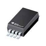
| 供应商器件封装 | 8-TSSOP |
| 其它名称 | 296-20946-6 |
| 包装 | Digi-Reel® |
| 单位重量 | 39 mg |
| 商标 | Texas Instruments |
| 安装类型 | 表面贴装 |
| 安装风格 | SMD/SMT |
| 封装 | Reel |
| 封装/外壳 | 8-TSSOP(0.173",4.40mm 宽) |
| 封装/箱体 | TSSOP-8 |
| 工作温度 | -40°C ~ 85°C |
| 工作温度范围 | - 40 C to + 85 C |
| 工作电流 | 1 mA |
| 工作电源电压 | 2.3 V to 3.6 V |
| 工厂包装数量 | 2000 |
| 应用 | I²C |
| 延迟时间 | - |
| 数据速率(最大值) | 400kHz |
| 最大时钟频率 | 400 kHz |
| 标准包装 | 1 |
| 电压-电源 | 2.3 V ~ 3.6 V |
| 电容-输入 | 7pF |
| 电流-电源 | 500µA |
| 类型 | 缓冲器, 转接驱动器 |
| 系列 | PCA9515A |
| 输入 | 2 线式总线 |
| 输入电容 | 7 pF |
| 输出 | 2 线式总线 |
| 通道数 | 1 |
| 逻辑类型 | I2C Bus, SMBus |
| 配用 | /product-detail/zh/OM6278,598/568-4002-ND/1213120 |


- 商务部:美国ITC正式对集成电路等产品启动337调查
- 曝三星4nm工艺存在良率问题 高通将骁龙8 Gen1或转产台积电
- 太阳诱电将投资9.5亿元在常州建新厂生产MLCC 预计2023年完工
- 英特尔发布欧洲新工厂建设计划 深化IDM 2.0 战略
- 台积电先进制程称霸业界 有大客户加持明年业绩稳了
- 达到5530亿美元!SIA预计今年全球半导体销售额将创下新高
- 英特尔拟将自动驾驶子公司Mobileye上市 估值或超500亿美元
- 三星加码芯片和SET,合并消费电子和移动部门,撤换高东真等 CEO
- 三星电子宣布重大人事变动 还合并消费电子和移动部门
- 海关总署:前11个月进口集成电路产品价值2.52万亿元 增长14.8%


PDF Datasheet 数据手册内容提取
Product Sample & Technical Tools & Support & Folder Buy Documents Software Community PCA9515A SCPS150D–DECEMBER2005–REVISEDJUNE2014 2 Dual Bidirectional I C Bus and SMBus Repeater 1 Features The I2C bus capacitance limit of 400 pF restricts the number of devices and bus length. Using the • Two-ChannelBidirectionalBuffers 1 PCA9515A enables the system designer to isolate • I2CBusandSMBusCompatible two halves of a bus, accommodating more I2C • Active-HighRepeater-EnableInput devicesorlongertracelengths. • Open-DrainI2CI/O The PCA9515A has an active-high enable (EN) input • 5.5-VTolerantI2CI/OandEnableInputSupport withaninternalpullup,whichallowstheusertoselect when the repeater is active. This can be used to Mixed-ModeSignalOperation isolate a badly behaved slave on power-up reset. It • Lockup-FreeOperation never should change state during an I2C operation, • AccommodatesStandardModeandFastMode because disabling during a bus operation hangs the I2CDevicesandMultipleMasters bus, and enabling part way through a bus cycle could • Powered-OffHigh-ImpedanceI2CPins confuse the I2C parts being enabled. The EN input should change state only when the global bus and • Latch-UpPerformanceExceeds100mAPer the repeater port are in an idle state, to prevent JESD78,ClassII systemfailures. • ESDProtectionExceedsJESD22 The PCA9515A also can be used to run two buses: – 2000-VHuman-BodyModel(A114-A) one at 5-V interface levels and the other at 3.3-V – 200-VMachineModel(A115-A) interface levels, or one at 400-kHz operating frequency and the other at 100-kHz operating – 1000-VCharged-DeviceModel(C101) frequency. If the two buses are operating at different frequencies, the 100-kHz bus must be isolated when 2 Description the 400-kHz operation of the other bus is required. If This dual bidirectional I2C buffer is operational at 2.3- the master is running at 400 kHz, the maximum Vto3.6-VV . CC system operating frequency may be less than The PCA9515A is a BiCMOS integrated circuit 400kHz,becauseofthedelaysthatareaddedbythe intended for I2C bus and SMBus systems repeater. applications. The device contains two identical The PCA9515A does not support clock stretching bidirectional open-drain buffer circuits that enable I2C acrosstherepeater. and similar bus systems to be extended without degradationofsystemperformance. DeviceInformation(1) The PCA9515A buffers both the serial data (SDA) PARTNUMBER PACKAGE BODYSIZE(NOM) and serial clock (SCL) signals on the I2C bus, while SOIC(8) 4.90mm×3.91mm retaining all the operating modes and features of the PCA9515A SON(8) 3.00mm×3.00mm I2C system. This enables two buses of 400-pF bus capacitancetobeconnectedinanI2Capplication. (1) For all available packages, see the orderable addendum at theendofthedatasheet. D,DCT,DGK,OR PW PACKAGE (TOPVIEW) NC 1 8 VCC SCL0 2 7 SCL1 SDA0 3 6 SDA1 GND 4 5 EN DRG PACKAGE (TOPVIEW) NC 1 8 VCC SCL0 2 7 SCL1 SDA0 3 6 SDA1 GND 4 5 EN NC–No internal connection 1 An IMPORTANT NOTICE at the end of this data sheet addresses availability, warranty, changes, use in safety-critical applications, intellectualpropertymattersandotherimportantdisclaimers.PRODUCTIONDATA.
PCA9515A SCPS150D–DECEMBER2005–REVISEDJUNE2014 www.ti.com Table of Contents 1 Features.................................................................. 1 7 ParameterMeasurementInformation..................6 2 Description............................................................. 1 8 DetailedDescription.............................................. 7 3 RevisionHistory..................................................... 2 8.1 FunctionalBlockDiagram.........................................7 4 Description(Continued)........................................ 3 8.2 FeatureDescription...................................................7 5 PinConfigurationandFunctions......................... 3 8.3 DeviceFunctionalModes..........................................7 6 Specifications......................................................... 4 9 ApplicationandImplementation.......................... 8 6.1 AbsoluteMaximumRatings .....................................4 9.1 TypicalApplication ...................................................8 6.2 HandlingRatings......................................................4 10 DeviceandDocumentationSupport................... 9 6.3 RecommendedOperatingConditions.......................4 10.1 Trademarks.............................................................9 6.4 ElectricalCharacteristics...........................................5 10.2 ElectrostaticDischargeCaution..............................9 6.5 TimingRequirements................................................5 10.3 Glossary..................................................................9 6.6 SwitchingCharacteristics..........................................5 11 Mechanical,Packaging,andOrderable Information............................................................. 9 3 Revision History ChangesfromRevisionC(January2011)toRevisionD Page • AddedClockStretchingErratasection. ................................................................................................................................. 7 ChangesfromRevisionB(October2007)toRevisionC Page • Deletedallreferencestoarbitrationandclockstretchingsupport.Thisdoesnoteffectmin/maxspecifications.................. 1 2 SubmitDocumentationFeedback Copyright©2005–2014,TexasInstrumentsIncorporated ProductFolderLinks:PCA9515A
PCA9515A www.ti.com SCPS150D–DECEMBER2005–REVISEDJUNE2014 4 Description (Continued) The output low levels for each internal buffer are approximately 0.5 V, but the input voltage of each internal buffer must be 70 mV or more below the output low level, when the output internally is driven low. This prevents alockupconditionfromoccurringwhentheinputlowconditionisreleased. Two or more PCA9515A devices cannot be used in series. The PCA9515A design does not allow this configuration.Becausethereisnodirectionpin,slightlydifferentvalidlow-voltagelevelsareusedtoavoidlockup conditions between the input and the output of each repeater. A valid low applied at the input of a PCA9515A is propagated as a buffered low with a slightly higher value on the enabled outputs. When this buffered low is applied to another PCA9515A-type device in series, the second device does not recognize it as a valid low and doesnotpropagateitasabufferedlowagain. The device contains a power-up control circuit that sets an internal latch to prevent the output circuits from becomingactiveuntilV isatavalidlevel(V =2.3V). CC CC AswiththestandardI2Csystem,pullupresistorsarerequiredtoprovidethelogichighlevelsonthebufferedbus. The PCA9515A has standard open-collector configuration of the I2C bus. The size of these pullup resistors depends on the system, but each side of the repeater must have a pullup resistor. The device is designed to work with Standard Mode and Fast Mode I2C devices in addition to SMBus devices. Standard Mode I2C devices only specify 3 mA in a generic I2C system where Standard Mode devices and multiple masters are possible. Undercertainconditions,highterminationcurrentscanbeused. 5 Pin Configuration and Functions D,DCT,DGK,OR PW PACKAGE (TOPVIEW) NC 1 8 VCC SCL0 2 7 SCL1 SDA0 3 6 SDA1 GND 4 5 EN DRG PACKAGE (TOPVIEW) NC 1 8 VCC SCL0 2 7 SCL1 SDA0 3 6 SDA1 GND 4 5 EN NC–No internal connection PinFunctions PIN DESCRIPTION NAME NO. NC 1 Nointernalconnection SCL0 2 Serialclockbus0 SDA0 3 Serialdatabus0 GND 4 Supplyground EN 5 Active-highrepeaterenableinput SDA1 6 Serialdatabus1 SCL1 7 Serialclockbus1 V 8 Supplypower CC Copyright©2005–2014,TexasInstrumentsIncorporated SubmitDocumentationFeedback 3 ProductFolderLinks:PCA9515A
PCA9515A SCPS150D–DECEMBER2005–REVISEDJUNE2014 www.ti.com 6 Specifications 6.1 Absolute Maximum Ratings(1) overoperatingfree-airtemperaturerange(unlessotherwisenoted) MIN MAX UNIT V Supplyvoltagerange –0.5 7 V CC V Enableinputvoltagerange(2) –0.5 7 V I V I2Cbusvoltagerange(2) –0.5 7 V I/O I Inputclampcurrent V <0 –50 mA IK I I Outputclampcurrent V <0 –50 mA OK O I Continuousoutputcurrent ±50 mA O ContinuouscurrentthroughV orGND ±100 mA CC Dpackage 97 DCTpackage 220 θ Packagethermalimpedance(3) DGKpackage 172 °C/W JA DRGpackage TBD PWpackage 149 (1) StressesbeyondthoselistedunderAbsoluteMaximumRatingsmaycausepermanentdamagetothedevice.Thesearestressratings only,andfunctionaloperationofthedeviceattheseoranyotherconditionsbeyondthoseindicatedunderRecommendedOperating Conditionsisnotimplied.Exposuretoabsolute-maximum-ratedconditionsforextendedperiodsmayaffectdevicereliability. (2) Theinputnegative-voltageandoutputvoltageratingsmaybeexceedediftheinputandoutputcurrentratingsareobserved. (3) ThepackagethermalimpedanceiscalculatedinaccordancewithJESD51-7. 6.2 Handling Ratings MIN MAX UNIT T Storagetemperaturerange –65 150 °C stg Humanbodymodel(HBM),perANSI/ESDA/JEDECJS-001,all pins(1) 0 2000 V Electrostaticdischarge V (ESD) Chargeddevicemodel(CDM),perJEDECspecification JESD22-C101,allpins(2) 0 1000 (1) JEDECdocumentJEP155statesthat500-VHBMallowssafemanufacturingwithastandardESDcontrolprocess. (2) JEDECdocumentJEP157statesthat250-VCDMallowssafemanufacturingwithastandardESDcontrolprocess. 6.3 Recommended Operating Conditions MIN MAX UNIT V Supplyvoltage 2.3 3.6 V CC SDAandSCLinputs 0.7×V 5.5 CC V High-levelinputvoltage V IH ENinput 2 5.5 SDAandSCLinputs –0.5 0.3×V V (1) Low-levelinputvoltage CC V IL ENinput –0.5 0.8 V (1) SDAandSCLlow-levelinputvoltagecontention –0.5 0.4 V ILc V =2.3V 6 CC I Low-leveloutputcurrent mA OL V =3V 6 CC T Operatingfree-airtemperature –40 85 °C A (1) V specificationisfortheENinputandthefirstlowlevelseenbytheSDAxandSCLxlines.V isforthesecondandsubsequentlow IL ILc levelsseenbytheSDAxandSCLxlines.V mustbeatleast70mVbelowV . ILc OL 4 SubmitDocumentationFeedback Copyright©2005–2014,TexasInstrumentsIncorporated ProductFolderLinks:PCA9515A
PCA9515A www.ti.com SCPS150D–DECEMBER2005–REVISEDJUNE2014 6.4 Electrical Characteristics overrecommendedoperatingfree-airtemperaturerange(unlessotherwisenoted) PARAMETER TESTCONDITIONS V MIN TYP(1) MAX UNIT CC V Inputdiodeclampvoltage I =–18mA 2.3Vto3.6V –1.2 V IK I SDAx, V Low-leveloutputvoltage I =20μAor6mA 2.3Vto3.6V 0.47 0.52 0.6 V OL SCLx OL Low-levelinputvoltagebelow SDAx, V –V I =10μA 2.3Vto3.6V 70 mV OL ILc low-leveloutputvoltage SCLx I Bothchannelshigh, 2.7V 0.5 3 SDAx=SCLx=VCC 3.6V 0.5 3 Bothchannelslow, 2.7V 1 4 SDA0=SCL0=GNDand I Quiescentsupplycurrent SDA1=SCL1=open;or mA CC SDA0=SCL0=openand 3.6V 1 4 SDA1=SCL1=GND Incontention, 2.7V 1 4 SDAx=SCLx=GND 3.6V 1 4 SDAx, VI=3.6V ±1 SCLx V =0.2V 3 I I Inputcurrent 2.3Vto3.6V μA I V =V ±1 I CC EN V =0.2V –10 –20 I SDAx, VI=3.6V 0.5 I Leakagecurrent EN=LorH 0V μA off SCLx V =GND 0.5 I Leakagecurrentduring SDAx, I V =3.6V EN=LorH 0Vto2.3V 1 μA I(ramp) powerup SCLx I EN 3.3V 7 9 Cin Inputcapacitance SDAx, VI=3VorGND pF EN=H 3.3V 7 9 SCLx (1) Alltypicalvaluesareatnominalsupplyvoltage(V =2.5Vor3.3V)andT =25°C. CC A 6.5 Timing Requirements overrecommendedoperatingfree-airtemperaturerange(unlessotherwisenoted)(seeFigure1) V =2.5V V =3.3V CC CC ±0.2V ±0.3V UNIT MIN MAX MIN MAX t Setuptime,EN↑beforeStartcondition 100 100 ns su t Holdtime,EN↓afterStopcondition 130 100 ns h 6.6 Switching Characteristics overrecommendedoperatingfree-airtemperaturerange,C ≤100pF(unlessotherwisenoted) L FROM TO VCC=2.5V±0.2V VCC=3.3V±0.3V PARAMETER UNIT (INPUT) (OUTPUT) MIN TYP(1) MAX MIN TYP(1) MAX tPZL Propagationdelaytime(2) SDA0,SCL0or SDA1,SCL1or 45 82 130 45 68 120 ns t SDA1,SCL1 SDA0,SCL0 33 113 190 33 102 180 PLZ ttHL Outputtransitiontime(2) 80% 20% 57 58 ns t (SDAx,SCLx) 20% 80% 148 147 tLH (1) Alltypicalvaluesareatnominalsupplyvoltage(V =2.5Vor3.3V)andT =25°C. CC A (2) DifferentloadresistanceandcapacitancealtertheRCtimeconstant,therebychangingthepropagationdelayandtransitiontimes. Copyright©2005–2014,TexasInstrumentsIncorporated SubmitDocumentationFeedback 5 ProductFolderLinks:PCA9515A
PCA9515A SCPS150D–DECEMBER2005–REVISEDJUNE2014 www.ti.com 7 Parameter Measurement Information VCC VCC PULSE VIN VOUT RL= 1.35 kΩ S1 DUT GENERATOR GND RT CL= 50 pF (see Note A) (see Note B) TEST S1 tPLZ/tPZL VCC TEST CIRCUIT FOR OPEN-DRAIN OUTPUT Input VCC 1.5V 1.5V 0V tPZL tPLZ Output VCC 80% 80% 1.5V 1.5V 20% 20% VOL ttHL ttLH VOLTAGEWAVEFORMS PROPAGATION DELAY AND OUTPUTTRANSITIONTIMES A. R terminationresistanceshouldbeequaltoZ ofpulsegenerators. T OUT B. C includesprobeandjigcapacitance. L C. All input pulses are supplied by generators having the following characteristics: PRR ≤ 10 MHz, Z = 50 Ω, O slewrate≥1V/ns. D. Theoutputsaremeasuredoneatatime,withonetransitionpermeasurement. E. t andt arethesameast . PLH PHL pd F. t andt arethesameast . PLZ PHZ dis G. t andt arethesameast . PZL PZH en Figure1. TestCircuitandVoltageWaveforms 6 SubmitDocumentationFeedback Copyright©2005–2014,TexasInstrumentsIncorporated ProductFolderLinks:PCA9515A
PCA9515A www.ti.com SCPS150D–DECEMBER2005–REVISEDJUNE2014 8 Detailed Description 8.1 Functional Block Diagram VCC 8 PCA9515A 3 6 SDA0 SDA1 2 7 SCL0 SCL1 Pullup Resistor 5 EN 4 Figure2. LogicDiagram(PositiveLogic) 8.2 Feature Description 8.2.1 ClockStretchingErrata Description Due to the static offset on both sides of the buffer (SCLx & SDAx) and the possibility of an overshoot above 500 mVduringeventslikeclockstretching,thedeviceshouldnotbeusedwithrisetimeaccelerators. SystemImpact Anincorrectlogicstatewillbepassedthroughthebuffer,creatinganI2Ccommunicationfailureonthebus. SystemWorkaround ThereisapossibleworkaroundtoavoidanI2Ccommunicationfailure: • Donotuserise-timeacceleratorsinconjunctionwiththePCA9515A. 8.3 Device Functional Modes Table1.FunctionTable INPUT FUNCTION EN L Outputsdisabled SDA0=SDA1 H SCL0=SCL1 Copyright©2005–2014,TexasInstrumentsIncorporated SubmitDocumentationFeedback 7 ProductFolderLinks:PCA9515A
PCA9515A SCPS150D–DECEMBER2005–REVISEDJUNE2014 www.ti.com 9 Application and Implementation 9.1 Typical Application AtypicalapplicationisshowninFigure3.Inthisexample,thesystemmasterisrunningona3.3-Vbus,whilethe slave is connected to a 5-V bus. Both buses run at 100 kHz, unless the slave bus is isolated, and then the masterbuscanrunat400kHz.Masterdevicescanbeplacedoneitherbus. 3.3V 5V SDA SDA0 SDA1 SDA SCL SCL0 SCL1 SCL PCA9515A I2C BUS MASTER I2C BUS SLAVE 400 kHz EN 100 kHz BUS 0 BUS 1 Figure3. TypicalApplication 9.1.1 DesignRequirements The PCA9515A is 5.5-V tolerant, so it does not require any additional circuitry to translate between the different busvoltages. When one side of the PCA9515A is pulled low by a device on the I2C bus, a CMOS hysteresis-type input detects the falling edge and causes an internal driver on the other side to turn on, thus causing the other side also to go low.ThesidedrivenlowbythePCA9515AtypicallyisatV =0.5V. OL 9.1.2 DetailedDesignProcedure Figure 4 and Figure 5 show the waveforms that are seen in a typical application. If the bus master in Figure 3 writes to the slave through the PCA9515A, Bus 0 has the waveform shown in Figure 4. This looks like a normal I2C transmission until the falling edge of the eighth clock pulse. At that point, the master releases the data line (SDA) while the slave pulls it low through the PCA9515A. Because the V of the PCA9515A typically is around OL 0.5 V, a step in the SDA is seen. After the master has transmitted the ninth clock pulse, the slave releases the dataline. 9th Clock Pulse SCL SDA V of Master V of PCA9515A OL OL Figure4. Bus0Waveforms 8 SubmitDocumentationFeedback Copyright©2005–2014,TexasInstrumentsIncorporated ProductFolderLinks:PCA9515A
PCA9515A www.ti.com SCPS150D–DECEMBER2005–REVISEDJUNE2014 Typical Application (continued) 9th Clock Pulse SCL SDA VOLof PCA9515A VOLof Slave Figure5. Bus1Waveforms On the Bus 1 side of the PCA9515A, the clock and data lines have a positive offset from ground equal to the V OL ofthePCA9515A.Aftertheeighthclockpulse,thedatalineispulledtotheV oftheslavedevice,whichisvery OL closetogroundintheexample. 10 Device and Documentation Support 10.1 Trademarks Alltrademarksarethepropertyoftheirrespectiveowners. 10.2 Electrostatic Discharge Caution Thesedeviceshavelimitedbuilt-inESDprotection.Theleadsshouldbeshortedtogetherorthedeviceplacedinconductivefoam duringstorageorhandlingtopreventelectrostaticdamagetotheMOSgates. 10.3 Glossary SLYZ022—TIGlossary. Thisglossarylistsandexplainsterms,acronyms,anddefinitions. 11 Mechanical, Packaging, and Orderable Information The following pages include mechanical, packaging, and orderable information. This information is the most current data available for the designated devices. This data is subject to change without notice and revision of thisdocument.Forbrowser-basedversionsofthisdatasheet,refertotheleft-handnavigation. Copyright©2005–2014,TexasInstrumentsIncorporated SubmitDocumentationFeedback 9 ProductFolderLinks:PCA9515A
PACKAGE OPTION ADDENDUM www.ti.com 6-Feb-2020 PACKAGING INFORMATION Orderable Device Status Package Type Package Pins Package Eco Plan Lead/Ball Finish MSL Peak Temp Op Temp (°C) Device Marking Samples (1) Drawing Qty (2) (6) (3) (4/5) PCA9515AD ACTIVE SOIC D 8 75 Green (RoHS NIPDAU Level-1-260C-UNLIM -40 to 85 PD515A & no Sb/Br) PCA9515ADGKR NRND VSSOP DGK 8 2500 Green (RoHS NIPDAU Level-1-260C-UNLIM -40 to 85 (7BA, 7BE) & no Sb/Br) PCA9515ADGKRG4 NRND VSSOP DGK 8 2500 Green (RoHS NIPDAU Level-1-260C-UNLIM -40 to 85 (7BA, 7BE) & no Sb/Br) PCA9515ADGKT NRND VSSOP DGK 8 250 Green (RoHS NIPDAU Level-1-260C-UNLIM -40 to 85 (7BA, 7BE) & no Sb/Br) PCA9515ADGKTG4 NRND VSSOP DGK 8 250 Green (RoHS NIPDAU Level-1-260C-UNLIM -40 to 85 (7BA, 7BE) & no Sb/Br) PCA9515ADR ACTIVE SOIC D 8 2500 Green (RoHS NIPDAU Level-1-260C-UNLIM -40 to 85 PD515A & no Sb/Br) PCA9515ADRGR ACTIVE SON DRG 8 3000 Green (RoHS NIPDAU Level-2-260C-1 YEAR -40 to 85 ZVD & no Sb/Br) PCA9515ADT ACTIVE SOIC D 8 250 Green (RoHS NIPDAU Level-1-260C-UNLIM -40 to 85 PD515A & no Sb/Br) PCA9515APW ACTIVE TSSOP PW 8 150 Green (RoHS NIPDAU Level-1-260C-UNLIM -40 to 85 PD515A & no Sb/Br) PCA9515APWR ACTIVE TSSOP PW 8 2000 Green (RoHS NIPDAU Level-1-260C-UNLIM -40 to 85 PD515A & no Sb/Br) PCA9515APWT ACTIVE TSSOP PW 8 250 Green (RoHS NIPDAU Level-1-260C-UNLIM -40 to 85 PD515A & no Sb/Br) (1) The marketing status values are defined as follows: ACTIVE: Product device recommended for new designs. LIFEBUY: TI has announced that the device will be discontinued, and a lifetime-buy period is in effect. NRND: Not recommended for new designs. Device is in production to support existing customers, but TI does not recommend using this part in a new design. PREVIEW: Device has been announced but is not in production. Samples may or may not be available. OBSOLETE: TI has discontinued the production of the device. (2) RoHS: TI defines "RoHS" to mean semiconductor products that are compliant with the current EU RoHS requirements for all 10 RoHS substances, including the requirement that RoHS substance do not exceed 0.1% by weight in homogeneous materials. Where designed to be soldered at high temperatures, "RoHS" products are suitable for use in specified lead-free processes. TI may reference these types of products as "Pb-Free". RoHS Exempt: TI defines "RoHS Exempt" to mean products that contain lead but are compliant with EU RoHS pursuant to a specific EU RoHS exemption. Green: TI defines "Green" to mean the content of Chlorine (Cl) and Bromine (Br) based flame retardants meet JS709B low halogen requirements of <=1000ppm threshold. Antimony trioxide based flame retardants must also meet the <=1000ppm threshold requirement. Addendum-Page 1
PACKAGE OPTION ADDENDUM www.ti.com 6-Feb-2020 (3) MSL, Peak Temp. - The Moisture Sensitivity Level rating according to the JEDEC industry standard classifications, and peak solder temperature. (4) There may be additional marking, which relates to the logo, the lot trace code information, or the environmental category on the device. (5) Multiple Device Markings will be inside parentheses. Only one Device Marking contained in parentheses and separated by a "~" will appear on a device. If a line is indented then it is a continuation of the previous line and the two combined represent the entire Device Marking for that device. (6) Lead/Ball Finish - Orderable Devices may have multiple material finish options. Finish options are separated by a vertical ruled line. Lead/Ball Finish values may wrap to two lines if the finish value exceeds the maximum column width. Important Information and Disclaimer:The information provided on this page represents TI's knowledge and belief as of the date that it is provided. TI bases its knowledge and belief on information provided by third parties, and makes no representation or warranty as to the accuracy of such information. Efforts are underway to better integrate information from third parties. TI has taken and continues to take reasonable steps to provide representative and accurate information but may not have conducted destructive testing or chemical analysis on incoming materials and chemicals. TI and TI suppliers consider certain information to be proprietary, and thus CAS numbers and other limited information may not be available for release. In no event shall TI's liability arising out of such information exceed the total purchase price of the TI part(s) at issue in this document sold by TI to Customer on an annual basis. Addendum-Page 2
PACKAGE MATERIALS INFORMATION www.ti.com 29-Sep-2019 TAPE AND REEL INFORMATION *Alldimensionsarenominal Device Package Package Pins SPQ Reel Reel A0 B0 K0 P1 W Pin1 Type Drawing Diameter Width (mm) (mm) (mm) (mm) (mm) Quadrant (mm) W1(mm) PCA9515ADGKR VSSOP DGK 8 2500 330.0 12.4 5.3 3.3 1.3 8.0 12.0 Q1 PCA9515ADGKR VSSOP DGK 8 2500 330.0 12.4 5.3 3.4 1.4 8.0 12.0 Q1 PCA9515ADGKT VSSOP DGK 8 250 180.0 12.4 5.3 3.3 1.3 8.0 12.0 Q1 PCA9515ADGKT VSSOP DGK 8 250 330.0 12.4 5.3 3.4 1.4 8.0 12.0 Q1 PCA9515ADR SOIC D 8 2500 330.0 12.4 6.4 5.2 2.1 8.0 12.0 Q1 PCA9515ADRGR SON DRG 8 3000 330.0 12.4 3.3 3.3 1.1 8.0 12.0 Q2 PCA9515ADT SOIC D 8 250 180.0 12.4 6.4 5.2 2.1 8.0 12.0 Q1 PCA9515APWR TSSOP PW 8 2000 330.0 12.4 7.0 3.6 1.6 8.0 12.0 Q1 PCA9515APWT TSSOP PW 8 250 330.0 12.4 7.0 3.6 1.6 8.0 12.0 Q1 PackMaterials-Page1
PACKAGE MATERIALS INFORMATION www.ti.com 29-Sep-2019 *Alldimensionsarenominal Device PackageType PackageDrawing Pins SPQ Length(mm) Width(mm) Height(mm) PCA9515ADGKR VSSOP DGK 8 2500 346.0 346.0 35.0 PCA9515ADGKR VSSOP DGK 8 2500 358.0 335.0 35.0 PCA9515ADGKT VSSOP DGK 8 250 220.0 205.0 50.0 PCA9515ADGKT VSSOP DGK 8 250 358.0 335.0 35.0 PCA9515ADR SOIC D 8 2500 367.0 367.0 35.0 PCA9515ADRGR SON DRG 8 3000 367.0 367.0 35.0 PCA9515ADT SOIC D 8 250 210.0 185.0 35.0 PCA9515APWR TSSOP PW 8 2000 367.0 367.0 35.0 PCA9515APWT TSSOP PW 8 250 367.0 367.0 35.0 PackMaterials-Page2
PACKAGE OUTLINE D0008A SOIC - 1.75 mm max height SCALE 2.800 SMALL OUTLINE INTEGRATED CIRCUIT C SEATING PLANE .228-.244 TYP [5.80-6.19] .004 [0.1] C A PIN 1 ID AREA 6X .050 [1.27] 8 1 2X .189-.197 [4.81-5.00] .150 NOTE 3 [3.81] 4X (0 -15 ) 4 5 8X .012-.020 B .150-.157 [0.31-0.51] .069 MAX [3.81-3.98] .010 [0.25] C A B [1.75] NOTE 4 .005-.010 TYP [0.13-0.25] 4X (0 -15 ) SEE DETAIL A .010 [0.25] .004-.010 0 - 8 [0.11-0.25] .016-.050 [0.41-1.27] DETAIL A (.041) TYPICAL [1.04] 4214825/C 02/2019 NOTES: 1. Linear dimensions are in inches [millimeters]. Dimensions in parenthesis are for reference only. Controlling dimensions are in inches. Dimensioning and tolerancing per ASME Y14.5M. 2. This drawing is subject to change without notice. 3. This dimension does not include mold flash, protrusions, or gate burrs. Mold flash, protrusions, or gate burrs shall not exceed .006 [0.15] per side. 4. This dimension does not include interlead flash. 5. Reference JEDEC registration MS-012, variation AA. www.ti.com
EXAMPLE BOARD LAYOUT D0008A SOIC - 1.75 mm max height SMALL OUTLINE INTEGRATED CIRCUIT 8X (.061 ) [1.55] SYMM SEE DETAILS 1 8 8X (.024) [0.6] SYMM (R.002 ) TYP [0.05] 5 4 6X (.050 ) [1.27] (.213) [5.4] LAND PATTERN EXAMPLE EXPOSED METAL SHOWN SCALE:8X SOLDER MASK SOLDER MASK METAL OPENING OPENING METAL UNDER SOLDER MASK EXPOSED METAL EXPOSED METAL .0028 MAX .0028 MIN [0.07] [0.07] ALL AROUND ALL AROUND NON SOLDER MASK SOLDER MASK DEFINED DEFINED SOLDER MASK DETAILS 4214825/C 02/2019 NOTES: (continued) 6. Publication IPC-7351 may have alternate designs. 7. Solder mask tolerances between and around signal pads can vary based on board fabrication site. www.ti.com
EXAMPLE STENCIL DESIGN D0008A SOIC - 1.75 mm max height SMALL OUTLINE INTEGRATED CIRCUIT 8X (.061 ) [1.55] SYMM 1 8 8X (.024) [0.6] SYMM (R.002 ) TYP [0.05] 5 4 6X (.050 ) [1.27] (.213) [5.4] SOLDER PASTE EXAMPLE BASED ON .005 INCH [0.125 MM] THICK STENCIL SCALE:8X 4214825/C 02/2019 NOTES: (continued) 8. Laser cutting apertures with trapezoidal walls and rounded corners may offer better paste release. IPC-7525 may have alternate design recommendations. 9. Board assembly site may have different recommendations for stencil design. www.ti.com
None
None
None
PACKAGE OUTLINE DRG0008A WSON - 0.8 mm max height SCALE 5.000 PLASTIC SMALL OUTLINE - NO LEAD 3.1 B A 2.9 3.1 PIN 1 INDEX AREA 2.9 0.8 0.7 C SEATING PLANE 0.05 0.00 0.08 C (0.2) TYP EXPOSED 1.2 0.1 THERMAL PAD 4 5 2X 1.5 2 0.1 8 1 6X 0.5 0.3 8X 0.2 PIN 1 ID 0.6 8X 0.1 C A B 0.4 0.08 C 4218885/A 03/2020 NOTES: 1. All linear dimensions are in millimeters. Any dimensions in parenthesis are for reference only. Dimensioning and tolerancing per ASME Y14.5M. 2. This drawing is subject to change without notice. 3. The package thermal pad must be soldered to the printed circuit board for thermal and mechanical performance. www.ti.com
EXAMPLE BOARD LAYOUT DRG0008A WSON - 0.8 mm max height PLASTIC SMALL OUTLINE - NO LEAD (1.2) 8X (0.7) SYMM 1 8 8X (0.25) SYMM (2) (0.75) 6X (0.5) 4 5 (R0.05) TYP ( 0.2) VIA (0.35) TYP (2.7) LAND PATTERN EXAMPLE EXPOSED METAL SHOWN SCALE:20X 0.07 MAX 0.07 MIN ALL AROUND ALL AROUND EXPOSED EXPOSED METAL METAL SOLDER MASK METAL METAL UNDER SOLDER MASK OPENING SOLDER MASK OPENING NON SOLDER MASK SOLDER MASK DEFINED DEFINED (PREFERRED) SOLDER MASK DETAILS 4218885/A 03/2020 NOTES: (continued) 4. This package is designed to be soldered to a thermal pad on the board. For more information, see Texas Instruments literature number SLUA271 (www.ti.com/lit/slua271). 5. Vias are optional depending on application, refer to device data sheet. If any vias are implemented, refer to their locations shown on this view. It is recommended that vias under paste be filled, plugged or tented. www.ti.com
EXAMPLE STENCIL DESIGN DRG0008A WSON - 0.8 mm max height PLASTIC SMALL OUTLINE - NO LEAD SYMM 8X (0.7) METAL TYP 8X (0.25) 1 8 SYMM (1.79) 6X (0.5) 4 5 (R0.05) TYP (1.13) (2.7) SOLDER PASTE EXAMPLE BASED ON 0.125 mm THICK STENCIL EXPOSED PAD 84% PRINTED SOLDER COVERAGE BY AREA SCALE:25X 4218885/A 03/2020 NOTES: (continued) 6. Laser cutting apertures with trapezoidal walls and rounded corners may offer better paste release. IPC-7525 may have alternate design recommendations. www.ti.com
PACKAGE OUTLINE PW0008A TSSOP - 1.2 mm max height SCALE 2.800 SMALL OUTLINE PACKAGE C 6.6 TYP SEATING PLANE 6.2 PIN 1 ID A 0.1 C AREA 6X 0.65 8 1 3.1 2X 2.9 NOTE 3 1.95 4 5 0.30 8X 0.19 4.5 1.2 MAX B 0.1 C A B 4.3 NOTE 4 (0.15) TYP SEE DETAIL A 0.25 GAGE PLANE 0.15 0.75 0 - 8 0.05 0.50 DETAIL A TYPICAL 4221848/A 02/2015 NOTES: 1. All linear dimensions are in millimeters. Any dimensions in parenthesis are for reference only. Dimensioning and tolerancing per ASME Y14.5M. 2. This drawing is subject to change without notice. 3. This dimension does not include mold flash, protrusions, or gate burrs. Mold flash, protrusions, or gate burrs shall not exceed 0.15 mm per side. 4. This dimension does not include interlead flash. Interlead flash shall not exceed 0.25 mm per side. 5. Reference JEDEC registration MO-153, variation AA. www.ti.com
EXAMPLE BOARD LAYOUT PW0008A TSSOP - 1.2 mm max height SMALL OUTLINE PACKAGE 8X (1.5) 8X (0.45) SYMM (R0.05) 1 TYP 8 SYMM 6X (0.65) 5 4 (5.8) LAND PATTERN EXAMPLE SCALE:10X SOOPLEDNEINRG MASK METAL MSOELTDAEL RU NMDAESRK SOOPLEDNEINRG MASK 0.05 MAX 0.05 MIN ALL AROUND ALL AROUND NON SOLDER MASK SOLDER MASK DEFINED DEFINED SOLDER MASK DETAILS NOT TO SCALE 4221848/A 02/2015 NOTES: (continued) 6. Publication IPC-7351 may have alternate designs. 7. Solder mask tolerances between and around signal pads can vary based on board fabrication site. www.ti.com
EXAMPLE STENCIL DESIGN PW0008A TSSOP - 1.2 mm max height SMALL OUTLINE PACKAGE 8X (1.5) SYMM (R0.05) TYP 8X (0.45) 1 8 SYMM 6X (0.65) 5 4 (5.8) SOLDER PASTE EXAMPLE BASED ON 0.125 mm THICK STENCIL SCALE:10X 4221848/A 02/2015 NOTES: (continued) 8. Laser cutting apertures with trapezoidal walls and rounded corners may offer better paste release. IPC-7525 may have alternate design recommendations. 9. Board assembly site may have different recommendations for stencil design. www.ti.com
IMPORTANTNOTICEANDDISCLAIMER TI PROVIDES TECHNICAL AND RELIABILITY DATA (INCLUDING DATASHEETS), DESIGN RESOURCES (INCLUDING REFERENCE DESIGNS), APPLICATION OR OTHER DESIGN ADVICE, WEB TOOLS, SAFETY INFORMATION, AND OTHER RESOURCES “AS IS” AND WITH ALL FAULTS, AND DISCLAIMS ALL WARRANTIES, EXPRESS AND IMPLIED, INCLUDING WITHOUT LIMITATION ANY IMPLIED WARRANTIES OF MERCHANTABILITY, FITNESS FOR A PARTICULAR PURPOSE OR NON-INFRINGEMENT OF THIRD PARTY INTELLECTUAL PROPERTY RIGHTS. These resources are intended for skilled developers designing with TI products. You are solely responsible for (1) selecting the appropriate TI products for your application, (2) designing, validating and testing your application, and (3) ensuring your application meets applicable standards, and any other safety, security, or other requirements. These resources are subject to change without notice. TI grants you permission to use these resources only for development of an application that uses the TI products described in the resource. Other reproduction and display of these resources is prohibited. No license is granted to any other TI intellectual property right or to any third party intellectual property right. TI disclaims responsibility for, and you will fully indemnify TI and its representatives against, any claims, damages, costs, losses, and liabilities arising out of your use of these resources. TI’s products are provided subject to TI’s Terms of Sale (www.ti.com/legal/termsofsale.html) or other applicable terms available either on ti.com or provided in conjunction with such TI products. TI’s provision of these resources does not expand or otherwise alter TI’s applicable warranties or warranty disclaimers for TI products. Mailing Address: Texas Instruments, Post Office Box 655303, Dallas, Texas 75265 Copyright © 2020, Texas Instruments Incorporated