ICGOO在线商城 > 集成电路(IC) > PMIC - 稳流/电流管理 > PAC1720-1-AIA-TR
 Datasheet下载
- 型号: PAC1720-1-AIA-TR
- 制造商: Microchip
- 库位|库存: xxxx|xxxx
- 要求:
| 数量阶梯 | 香港交货 | 国内含税 |
| +xxxx | $xxxx | ¥xxxx |
查看当月历史价格
查看今年历史价格
PAC1720-1-AIA-TR产品简介:
ICGOO电子元器件商城为您提供PAC1720-1-AIA-TR由Microchip设计生产,在icgoo商城现货销售,并且可以通过原厂、代理商等渠道进行代购。 PAC1720-1-AIA-TR价格参考。MicrochipPAC1720-1-AIA-TR封装/规格:PMIC - 稳流/电流管理, Current Monitor Regulator High-Side 10-DFN (3x3)。您可以下载PAC1720-1-AIA-TR参考资料、Datasheet数据手册功能说明书,资料中有PAC1720-1-AIA-TR 详细功能的应用电路图电压和使用方法及教程。
Microchip Technology的PAC1720-1-AIA-TR是一款电流检测监控器,属于PMIC(电源管理集成电路)中的稳流/电流管理类别。该器件主要用于实时监测直流电流和电压,并计算功率输出,具备高精度测量能力。

其典型应用场景包括:便携式设备(如智能手机、平板电脑)、电池供电系统、笔记本电脑和嵌入式系统中的电源管理。它可帮助系统实现功耗优化与热管理,提升能效并延长电池寿命。此外,该芯片也广泛用于工业控制设备、电信设备和服务器电源模块中,用于实时监控负载电流和系统功耗,支持故障检测与保护功能。

PAC1720-1-AIA-TR采用小型化封装,适合空间受限的设计,同时具备I²C/SMBus通信接口,便于与主控制器进行数据交互。其宽工作电压范围和低功耗特性,使其在多种电源轨监测应用中表现出色,如5V、3.3V或更低电压系统的电流采样。

总之,该芯片适用于需要精确电流、电压及功率监测的电子系统,尤其在节能管理、系统诊断和电源健康监控方面发挥重要作用。
| 参数 | 数值 |
| 产品目录 | 集成电路 (IC)半导体 |
| 描述 | IC CURRENT SENSE MON DUAL 10VDFN电流和电力监控器、调节器 Single I2C/SMBus Current Sensor |
| 产品分类 | |
| 品牌 | Microchip Technology |
| 产品手册 | |
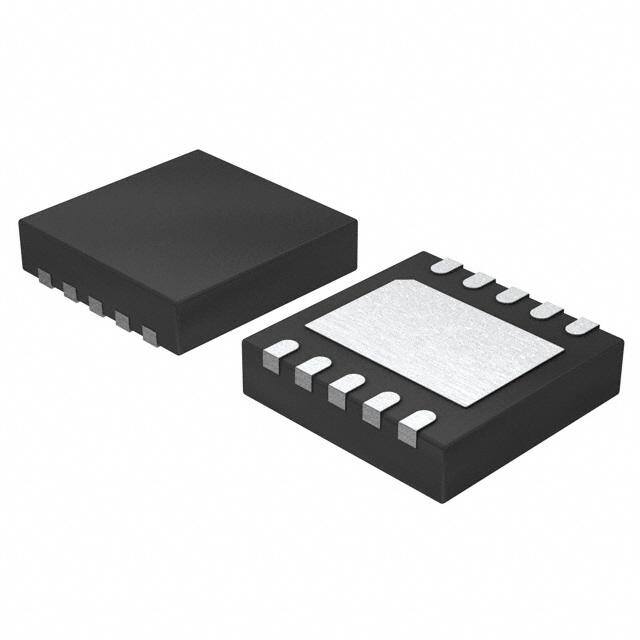
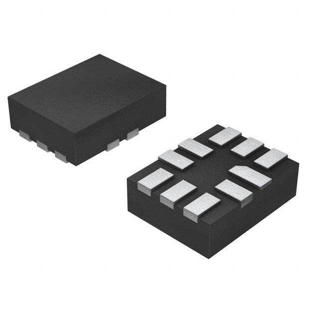
| 产品图片 |
|
| rohs | 符合RoHS无铅 / 符合限制有害物质指令(RoHS)规范要求 |
| 产品系列 | 电源管理 IC,电流和电力监控器、调节器,Microchip Technology PAC1720-1-AIA-TR- |
| 数据手册 | |
| 产品型号 | PAC1720-1-AIA-TR |
| 产品 | Current and Power Monitors |
| 产品种类 | 电流和电力监控器、调节器 |
| 供应商器件封装 | 10-DFN(3x3) |
| 其它名称 | PAC1720-1-AIA-CT |
| 准确性 | 1 % |
| 功能 | 电流感应 |
| 包装 | 剪切带 (CT) |
| 商标 | Microchip Technology |
| 安装类型 | 表面贴装 |
| 安装风格 | SMD/SMT |
| 封装 | Reel |
| 封装/外壳 | 10-VFDFN 裸露焊盘 |
| 封装/箱体 | DFN-10 |
| 工作温度 | -40°C ~ 85°C |
| 工作温度范围 | - 40 C to + 85 C |
| 工厂包装数量 | 4000 |
| 感应方式 | High Side |
| 感应方法 | 高端 |
| 标准包装 | 1 |
| 电压-输入 | 0 V ~ 40 V |
| 电流-输出 | - |
| 电源电压-最大 | 5.5 V |
| 电源电压-最小 | 3 V |
| 电源电流 | 0.525 mA |
| 精度 | ±1% |
| 输入电压范围 | 3 V to 5.5 V |


- 商务部:美国ITC正式对集成电路等产品启动337调查
- 曝三星4nm工艺存在良率问题 高通将骁龙8 Gen1或转产台积电
- 太阳诱电将投资9.5亿元在常州建新厂生产MLCC 预计2023年完工
- 英特尔发布欧洲新工厂建设计划 深化IDM 2.0 战略
- 台积电先进制程称霸业界 有大客户加持明年业绩稳了
- 达到5530亿美元!SIA预计今年全球半导体销售额将创下新高
- 英特尔拟将自动驾驶子公司Mobileye上市 估值或超500亿美元
- 三星加码芯片和SET,合并消费电子和移动部门,撤换高东真等 CEO
- 三星电子宣布重大人事变动 还合并消费电子和移动部门
- 海关总署:前11个月进口集成电路产品价值2.52万亿元 增长14.8%


PDF Datasheet 数据手册内容提取
PAC1720 Dual High-Side Current Sense Monitor with Power Calculation PRODUCT FEATURES Datasheet General Description Features The PAC1720 is a dual high-side bi-directional current (cid:132) Dual high-side current sensor sensing monitor with precision voltage measurement — Current measurement is integrated over 2.5ms to capabilities. Each sensor measures the voltage 2.6sec with up to 11-bit resolution developed across an external sense resistor to — 1% current measurement accuracy in positive range represent the high-side current of a battery or voltage — Measures VSOURCE voltages regulator. The PAC1720 also measures the SENSE+ pin (cid:132) Calculates proportional power voltage and calculates average power over the (cid:132) VSOURCE voltage range 0V to 40V integration period. The PAC1720 can be programmed to — Bi-directional current sensing assert the ALERT pin when high and low limits are (cid:132) Auto-zero input offset voltage exceeded for Current Sense and Bus Voltage. (cid:132) Digital averaging Available in a RoHS compliant 3 X 3mm 10-pin DFN — Adjustable sampling time and resolution package. (cid:132) 5µA typical Standby current The PAC1720 device is good for measuring dynamic (cid:132) Programmable sense voltage range power. The long integration time allows for extending — ±10mV, ±20mV, ±40mV, and ±80mV system polling cycles without losing any power (cid:132) Power supply range 3.0V to 5.5V consumption information. In addition the alert ensures (cid:132) Wide temperature operating range: -40°C to +85°C that transient events are captured between the polling (cid:132) ALERT output for voltage and current out of limit cycles. transients between sampling interval Applications (cid:132) SMBus 2.0 communications interface — Address selectable by resistor decode (cid:132) Notebook and Desktop Computers (cid:132) Industrial (cid:132) S—amWpliteh taimveera cgoinngf igefuferactbivlee sfraommp li2n.g5 mtimse-3s 2u0pm tos 2.6sec (cid:132) Power Management Systems (cid:132) 3x3 mm DFN-10 package (cid:132) Embedded Applications Block Diagram E1+ E1- E2+ E2- S S S S N N N N D E E E E D S S S S V Power Management ADDR_SEL CurrentLimits Current Current Measurement Measurement CurrentRegisters SMBus SMCLK Interface SMDATA Analog MUX Configuration Configuration Power Register ALERT Voltage Registers Voltage Voltage Measurement Measurement Voltage Limits GND SMSC PAC1720 SMSC CONFIDENTIAL DATASHEET Revision 1.1 (12-08-11)
Dual High-Side Current Sense Monitor with Power Calculation Datasheet Ordering Information: ORDERING NUMBER PACKAGE FEATURES PAC1720-1-AIA-TR 10-pin 3 X 3 DFN SMBus 2.0 communications (Lead Free RoHS compliant) interface, ALERT pin, dual sensor REEL SIZE IS 4,000 PIECES This product meets the halogen maximum concentration values per IEC61249-2-21 For RoHS compliance and environmental information, please visit www.smsc.com/rohs 80 ARKAY DRIVE, HAUPPAUGE, NY 11788 (631) 435-6000 or 1 (800) 443-SEMI Copyright © 2011 SMSC or its subsidiaries. All rights reserved. Circuit diagrams and other information relating to SMSC products are included as a means of illustrating typical applications. Consequently, complete information sufficient for construction purposes is not necessarily given. Although the information has been checked and is believed to be accurate, no responsibility is assumed for inaccuracies. SMSC reserves the right to make changes to specifications and product descriptions at any time without notice. Contact your local SMSC sales office to obtain the latest specifications before placing your product order. The provision of this information does not convey to the purchaser of the described semiconductor devices any licenses under any patent rights or other intellectual property rights of SMSC or others. All sales are expressly conditional on your agreement to the terms and conditions of the most recently dated version of SMSC's standard Terms of Sale Agreement dated before the date of your order (the "Terms of Sale Agreement"). The product may contain design defects or errors known as anomalies which may cause the product's functions to deviate from published specifications. Anomaly sheets are available upon request. SMSC products are not designed, intended, authorized or warranted for use in any life support or other application where product failure could cause or contribute to personal injury or severe property damage. Any and all such uses without prior written approval of an Officer of SMSC and further testing and/or modification will be fully at the risk of the customer. Copies of this document or other SMSC literature, as well as the Terms of Sale Agreement, may be obtained by visiting SMSC’s website at http://www.smsc.com. SMSC is a registered trademark of Standard Microsystems Corporation (“SMSC”). Product names and company names are the trademarks of their respective holders. SMSC DISCLAIMS AND EXCLUDES ANY AND ALL WARRANTIES, INCLUDING WITHOUT LIMITATION ANY AND ALL IMPLIED WARRANTIES OF MERCHANTABILITY, FITNESS FOR A PARTICULAR PURPOSE, TITLE, AND AGAINST INFRINGEMENT AND THE LIKE, AND ANY AND ALL WARRANTIES ARISING FROM ANY COURSE OF DEALING OR USAGE OF TRADE. IN NO EVENT SHALL SMSC BE LIABLE FOR ANY DIRECT, INCIDENTAL, INDIRECT, SPECIAL, PUNITIVE, OR CONSEQUENTIAL DAMAGES; OR FOR LOST DATA, PROFITS, SAVINGS OR REVENUES OF ANY KIND; REGARDLESS OF THE FORM OF ACTION, WHETHER BASED ON CONTRACT; TORT; NEGLIGENCE OF SMSC OR OTHERS; STRICT LIABILITY; BREACH OF WARRANTY; OR OTHERWISE; WHETHER OR NOT ANY REMEDY OF BUYER IS HELD TO HAVE FAILED OF ITS ESSENTIAL PURPOSE, AND WHETHER OR NOT SMSC HAS BEEN ADVISED OF THE POSSIBILITY OF SUCH DAMAGES. Revision 1.1 (12-08-11) 2 SMSC PAC1720 SMSC CONFIDENTIAL DATASHEET
Dual High-Side Current Sense Monitor with Power Calculation Datasheet Table of Contents Chapter1 Pin Description. . . . . . . . . . . . . . . . . . . . . . . . . . . . . . . . . . . . . . . . . . . . . . . . . . . . . 7 Chapter2 Electrical Characteristics . . . . . . . . . . . . . . . . . . . . . . . . . . . . . . . . . . . . . . . . . . . . 9 2.1 Electrical Specifications . . . . . . . . . . . . . . . . . . . . . . . . . . . . . . . . . . . . . . . . . . . . . . . . . . . . . . . . . 10 2.2 SMBus Electrical Specifications. . . . . . . . . . . . . . . . . . . . . . . . . . . . . . . . . . . . . . . . . . . . . . . . . . . 12 Chapter3 Communications . . . . . . . . . . . . . . . . . . . . . . . . . . . . . . . . . . . . . . . . . . . . . . . . . . 14 3.1 System Management SMBus Interface Protocol . . . . . . . . . . . . . . . . . . . . . . . . . . . . . . . . . . . . . . 14 3.1.1 SMBus Start Bit. . . . . . . . . . . . . . . . . . . . . . . . . . . . . . . . . . . . . . . . . . . . . . . . . . . . . . . . 14 3.1.2 SMBus Address and RD / WR Bit . . . . . . . . . . . . . . . . . . . . . . . . . . . . . . . . . . . . . . . . . . 14 3.1.3 SMBus ACK and NACK Bits . . . . . . . . . . . . . . . . . . . . . . . . . . . . . . . . . . . . . . . . . . . . . . 15 3.1.4 SMBus Stop Bit. . . . . . . . . . . . . . . . . . . . . . . . . . . . . . . . . . . . . . . . . . . . . . . . . . . . . . . . 15 3.1.5 SMBus Timeout. . . . . . . . . . . . . . . . . . . . . . . . . . . . . . . . . . . . . . . . . . . . . . . . . . . . . . . . 15 3.1.6 SMBus and I2C Compliance . . . . . . . . . . . . . . . . . . . . . . . . . . . . . . . . . . . . . . . . . . . . . . 15 3.2 SMBus Protocols . . . . . . . . . . . . . . . . . . . . . . . . . . . . . . . . . . . . . . . . . . . . . . . . . . . . . . . . . . . . . . 16 3.2.1 Write Byte . . . . . . . . . . . . . . . . . . . . . . . . . . . . . . . . . . . . . . . . . . . . . . . . . . . . . . . . . . . . 16 3.2.2 Read Byte . . . . . . . . . . . . . . . . . . . . . . . . . . . . . . . . . . . . . . . . . . . . . . . . . . . . . . . . . . . . 16 3.2.3 Send Byte . . . . . . . . . . . . . . . . . . . . . . . . . . . . . . . . . . . . . . . . . . . . . . . . . . . . . . . . . . . . 16 3.2.4 Receive Byte. . . . . . . . . . . . . . . . . . . . . . . . . . . . . . . . . . . . . . . . . . . . . . . . . . . . . . . . . . 17 3.2.5 Alert Response Address . . . . . . . . . . . . . . . . . . . . . . . . . . . . . . . . . . . . . . . . . . . . . . . . . 17 3.3 I2C Protocols. . . . . . . . . . . . . . . . . . . . . . . . . . . . . . . . . . . . . . . . . . . . . . . . . . . . . . . . . . . . . . . . . . 17 3.3.1 Block Write . . . . . . . . . . . . . . . . . . . . . . . . . . . . . . . . . . . . . . . . . . . . . . . . . . . . . . . . . . . 17 3.3.2 Block Read . . . . . . . . . . . . . . . . . . . . . . . . . . . . . . . . . . . . . . . . . . . . . . . . . . . . . . . . . . . 18 Chapter4 General Description. . . . . . . . . . . . . . . . . . . . . . . . . . . . . . . . . . . . . . . . . . . . . . . . 19 4.1 Power States . . . . . . . . . . . . . . . . . . . . . . . . . . . . . . . . . . . . . . . . . . . . . . . . . . . . . . . . . . . . . . . . . 19 4.2 Conversion Cycle . . . . . . . . . . . . . . . . . . . . . . . . . . . . . . . . . . . . . . . . . . . . . . . . . . . . . . . . . . . . . . 20 4.2.1 Conversion Rate . . . . . . . . . . . . . . . . . . . . . . . . . . . . . . . . . . . . . . . . . . . . . . . . . . . . . . . 20 4.3 Current Measurement. . . . . . . . . . . . . . . . . . . . . . . . . . . . . . . . . . . . . . . . . . . . . . . . . . . . . . . . . . . 20 4.4 Voltage Measurement. . . . . . . . . . . . . . . . . . . . . . . . . . . . . . . . . . . . . . . . . . . . . . . . . . . . . . . . . . . 21 4.5 Power Calculation. . . . . . . . . . . . . . . . . . . . . . . . . . . . . . . . . . . . . . . . . . . . . . . . . . . . . . . . . . . . . . 22 4.6 ALERT Output . . . . . . . . . . . . . . . . . . . . . . . . . . . . . . . . . . . . . . . . . . . . . . . . . . . . . . . . . . . . . . . . 23 Chapter5 Register Descriptions. . . . . . . . . . . . . . . . . . . . . . . . . . . . . . . . . . . . . . . . . . . . . . . 24 5.1 Data Read Interlock . . . . . . . . . . . . . . . . . . . . . . . . . . . . . . . . . . . . . . . . . . . . . . . . . . . . . . . . . . . . 25 5.2 Configuration Register . . . . . . . . . . . . . . . . . . . . . . . . . . . . . . . . . . . . . . . . . . . . . . . . . . . . . . . . . . 26 5.3 Conversion Rate Register. . . . . . . . . . . . . . . . . . . . . . . . . . . . . . . . . . . . . . . . . . . . . . . . . . . . . . . . 27 5.4 One-Shot Register . . . . . . . . . . . . . . . . . . . . . . . . . . . . . . . . . . . . . . . . . . . . . . . . . . . . . . . . . . . . . 27 5.5 Mask Register. . . . . . . . . . . . . . . . . . . . . . . . . . . . . . . . . . . . . . . . . . . . . . . . . . . . . . . . . . . . . . . . . 28 5.6 High Limit Status Register . . . . . . . . . . . . . . . . . . . . . . . . . . . . . . . . . . . . . . . . . . . . . . . . . . . . . . . 29 5.7 Low Limit Status Register. . . . . . . . . . . . . . . . . . . . . . . . . . . . . . . . . . . . . . . . . . . . . . . . . . . . . . . . 29 5.8 VSOURCE Sampling Configuration Register. . . . . . . . . . . . . . . . . . . . . . . . . . . . . . . . . . . . . . . . . 30 5.9 VSENSE Sampling Configuration Registers. . . . . . . . . . . . . . . . . . . . . . . . . . . . . . . . . . . . . . . . . . 31 5.9.1 CH1 VSENSE Sampling Configuration - 0Bh . . . . . . . . . . . . . . . . . . . . . . . . . . . . . . . . . 31 5.9.2 CH2 VSENSE Sampling Configuration - 0Ch . . . . . . . . . . . . . . . . . . . . . . . . . . . . . . . . . 31 5.10 Sense Voltage Registers . . . . . . . . . . . . . . . . . . . . . . . . . . . . . . . . . . . . . . . . . . . . . . . . . . . . . . . . 32 5.11 VSOURCE Voltage Registers. . . . . . . . . . . . . . . . . . . . . . . . . . . . . . . . . . . . . . . . . . . . . . . . . . . . . 34 5.12 Power Ratio Registers . . . . . . . . . . . . . . . . . . . . . . . . . . . . . . . . . . . . . . . . . . . . . . . . . . . . . . . . . . 35 5.13 V Limit Registers. . . . . . . . . . . . . . . . . . . . . . . . . . . . . . . . . . . . . . . . . . . . . . . . . . . . . . . . . . 35 SENSE 5.14 VSOURCE Voltage Limit Registers . . . . . . . . . . . . . . . . . . . . . . . . . . . . . . . . . . . . . . . . . . . . . . . . 36 SMSC PAC1720 3 Revision 1.1 (12-08-11) SMSC CONFIDENTIAL DATASHEET
Dual High-Side Current Sense Monitor with Power Calculation Datasheet 5.15 Product ID Register . . . . . . . . . . . . . . . . . . . . . . . . . . . . . . . . . . . . . . . . . . . . . . . . . . . . . . . . . . . . 36 5.16 SMSC ID Register . . . . . . . . . . . . . . . . . . . . . . . . . . . . . . . . . . . . . . . . . . . . . . . . . . . . . . . . . . . . . 36 5.17 Revision Register . . . . . . . . . . . . . . . . . . . . . . . . . . . . . . . . . . . . . . . . . . . . . . . . . . . . . . . . . . . . . . 37 Chapter6 Package Description . . . . . . . . . . . . . . . . . . . . . . . . . . . . . . . . . . . . . . . . . . . . . . . 38 6.1 PAC1720 Package Drawing (10-Pin DFN). . . . . . . . . . . . . . . . . . . . . . . . . . . . . . . . . . . . . . . . . . . 38 6.2 PAC1720 Package Markings . . . . . . . . . . . . . . . . . . . . . . . . . . . . . . . . . . . . . . . . . . . . . . . . . . . . . 40 Chapter7 Application Usage . . . . . . . . . . . . . . . . . . . . . . . . . . . . . . . . . . . . . . . . . . . . . . . . . 41 7.1 Electrical Overstress. . . . . . . . . . . . . . . . . . . . . . . . . . . . . . . . . . . . . . . . . . . . . . . . . . . . . . . . . . . . 41 7.2 PAC1720 Internal Filtering . . . . . . . . . . . . . . . . . . . . . . . . . . . . . . . . . . . . . . . . . . . . . . . . . . . . . . . 42 7.3 Do Not Apply a Filter Across the Current Shunt. . . . . . . . . . . . . . . . . . . . . . . . . . . . . . . . . . . . . . . 42 7.4 Initial Device Configuration. . . . . . . . . . . . . . . . . . . . . . . . . . . . . . . . . . . . . . . . . . . . . . . . . . . . . . . 44 Chapter8 Typical Operating Curves. . . . . . . . . . . . . . . . . . . . . . . . . . . . . . . . . . . . . . . . . . . 45 Chapter9 Datasheet Revision History. . . . . . . . . . . . . . . . . . . . . . . . . . . . . . . . . . . . . . . . . . 47 Revision 1.1 (12-08-11) 4 SMSC PAC1720 SMSC CONFIDENTIAL DATASHEET
Dual High-Side Current Sense Monitor with Power Calculation Datasheet List of Figures Figure1.1 PAC1720 Pin Diagram. . . . . . . . . . . . . . . . . . . . . . . . . . . . . . . . . . . . . . . . . . . . . . . . . . . . . . . 7 Figure3.1 SMBus Timing Diagram. . . . . . . . . . . . . . . . . . . . . . . . . . . . . . . . . . . . . . . . . . . . . . . . . . . . . 14 Figure4.1 PAC1720 System Diagram . . . . . . . . . . . . . . . . . . . . . . . . . . . . . . . . . . . . . . . . . . . . . . . . . . 19 Figure6.1 10-Pin DFN Package Drawings. . . . . . . . . . . . . . . . . . . . . . . . . . . . . . . . . . . . . . . . . . . . . . . 38 Figure6.2 10-Pin DFN Package Dimensions . . . . . . . . . . . . . . . . . . . . . . . . . . . . . . . . . . . . . . . . . . . . . 39 Figure6.3 10-Pin DFN Recommended PCB Land Pattern. . . . . . . . . . . . . . . . . . . . . . . . . . . . . . . . . . . 39 Figure6.4 PAC1720 Package Marking. . . . . . . . . . . . . . . . . . . . . . . . . . . . . . . . . . . . . . . . . . . . . . . . . . 40 Figure7.1 Equivalent Internal ESD Circuitry. . . . . . . . . . . . . . . . . . . . . . . . . . . . . . . . . . . . . . . . . . . . . . 41 Figure7.2 PAC1720 with Unnecessary Filters on the Input Pins . . . . . . . . . . . . . . . . . . . . . . . . . . . . . . 43 Figure8.1 IDD Vs VDD. . . . . . . . . . . . . . . . . . . . . . . . . . . . . . . . . . . . . . . . . . . . . . . . . . . . . . . . . . . . . . 45 Figure8.2 IDD Vs VDD. . . . . . . . . . . . . . . . . . . . . . . . . . . . . . . . . . . . . . . . . . . . . . . . . . . . . . . . . . . . . . 45 Figure8.3 IDD Vs VDD. . . . . . . . . . . . . . . . . . . . . . . . . . . . . . . . . . . . . . . . . . . . . . . . . . . . . . . . . . . . . . 45 Figure8.4 ISENSE+ Pin Current Vs VBUS. . . . . . . . . . . . . . . . . . . . . . . . . . . . . . . . . . . . . . . . . . . . . . . 45 Figure8.5 ISENSE+ Pin Bias Current. . . . . . . . . . . . . . . . . . . . . . . . . . . . . . . . . . . . . . . . . . . . . . . . . . . 45 Figure8.6 ISENSE- Pin Bias Current . . . . . . . . . . . . . . . . . . . . . . . . . . . . . . . . . . . . . . . . . . . . . . . . . . . 45 Figure8.7 ISENSE+ Pin Leakage Current . . . . . . . . . . . . . . . . . . . . . . . . . . . . . . . . . . . . . . . . . . . . . . . 46 Figure8.8 ISENSE- Pin Leakage Current. . . . . . . . . . . . . . . . . . . . . . . . . . . . . . . . . . . . . . . . . . . . . . . . 46 Figure8.9 ISENSE+ Pin Current Vs VBUS. . . . . . . . . . . . . . . . . . . . . . . . . . . . . . . . . . . . . . . . . . . . . . . 46 SMSC PAC1720 5 Revision 1.1 (12-08-11) SMSC CONFIDENTIAL DATASHEET
Dual High-Side Current Sense Monitor with Power Calculation Datasheet List of Tables Table1.1 Pin Description for PAC1720. . . . . . . . . . . . . . . . . . . . . . . . . . . . . . . . . . . . . . . . . . . . . . . . . . . 7 Table1.2 Pin Types. . . . . . . . . . . . . . . . . . . . . . . . . . . . . . . . . . . . . . . . . . . . . . . . . . . . . . . . . . . . . . . . . . 8 Table2.1 Absolute Maximum Ratings. . . . . . . . . . . . . . . . . . . . . . . . . . . . . . . . . . . . . . . . . . . . . . . . . . . . 9 Table2.2 Electrical Specifications. . . . . . . . . . . . . . . . . . . . . . . . . . . . . . . . . . . . . . . . . . . . . . . . . . . . . . 10 Table2.3 SMBus Electrical Specifications . . . . . . . . . . . . . . . . . . . . . . . . . . . . . . . . . . . . . . . . . . . . . . . 12 Table3.1 ADDR_SEL Resistor Setting. . . . . . . . . . . . . . . . . . . . . . . . . . . . . . . . . . . . . . . . . . . . . . . . . . 15 Table3.2 Protocol Format. . . . . . . . . . . . . . . . . . . . . . . . . . . . . . . . . . . . . . . . . . . . . . . . . . . . . . . . . . . . 16 Table3.3 Write Byte Protocol . . . . . . . . . . . . . . . . . . . . . . . . . . . . . . . . . . . . . . . . . . . . . . . . . . . . . . . . . 16 Table3.4 Read Byte Protocol . . . . . . . . . . . . . . . . . . . . . . . . . . . . . . . . . . . . . . . . . . . . . . . . . . . . . . . . . 16 Table3.5 Send Byte Protocol . . . . . . . . . . . . . . . . . . . . . . . . . . . . . . . . . . . . . . . . . . . . . . . . . . . . . . . . . 17 Table3.6 Receive Byte Protocol. . . . . . . . . . . . . . . . . . . . . . . . . . . . . . . . . . . . . . . . . . . . . . . . . . . . . . . 17 Table3.7 Alert Response Address Protocol . . . . . . . . . . . . . . . . . . . . . . . . . . . . . . . . . . . . . . . . . . . . . . 17 Table3.8 Block Write Protocol . . . . . . . . . . . . . . . . . . . . . . . . . . . . . . . . . . . . . . . . . . . . . . . . . . . . . . . . 18 Table3.9 Block Read Protocol . . . . . . . . . . . . . . . . . . . . . . . . . . . . . . . . . . . . . . . . . . . . . . . . . . . . . . . . 18 Table5.1 Register Set in Hexadecimal Order. . . . . . . . . . . . . . . . . . . . . . . . . . . . . . . . . . . . . . . . . . . . . 24 Table5.2 Configuration Register. . . . . . . . . . . . . . . . . . . . . . . . . . . . . . . . . . . . . . . . . . . . . . . . . . . . . . . 26 Table5.3 Conversion Rate Register . . . . . . . . . . . . . . . . . . . . . . . . . . . . . . . . . . . . . . . . . . . . . . . . . . . . 27 Table5.4 Conversion Rate for Measurement . . . . . . . . . . . . . . . . . . . . . . . . . . . . . . . . . . . . . . . . . . . . . 27 Table5.5 One-Shot Register. . . . . . . . . . . . . . . . . . . . . . . . . . . . . . . . . . . . . . . . . . . . . . . . . . . . . . . . . . 27 Table5.6 Channel Mask Register. . . . . . . . . . . . . . . . . . . . . . . . . . . . . . . . . . . . . . . . . . . . . . . . . . . . . . 28 Table5.7 High Limit Status Register. . . . . . . . . . . . . . . . . . . . . . . . . . . . . . . . . . . . . . . . . . . . . . . . . . . . 29 Table5.8 Low Limit Status Register . . . . . . . . . . . . . . . . . . . . . . . . . . . . . . . . . . . . . . . . . . . . . . . . . . . . 29 Table5.9 Voltage Sampling Configuration Register . . . . . . . . . . . . . . . . . . . . . . . . . . . . . . . . . . . . . . . . 30 Table5.10Voltage Source Sampling Time Settings. . . . . . . . . . . . . . . . . . . . . . . . . . . . . . . . . . . . . . . . . 30 Table5.11Voltage Source Averaging Settings. . . . . . . . . . . . . . . . . . . . . . . . . . . . . . . . . . . . . . . . . . . . . 30 Table5.12VSENSE Sampling Configuration Registers . . . . . . . . . . . . . . . . . . . . . . . . . . . . . . . . . . . . . . 31 Table5.13Current Sensing Averaging Settings . . . . . . . . . . . . . . . . . . . . . . . . . . . . . . . . . . . . . . . . . . . . 31 Table5.14Current Sensing Sampling Time Settings . . . . . . . . . . . . . . . . . . . . . . . . . . . . . . . . . . . . . . . . 32 Table5.15Current Sensing Range Settings. . . . . . . . . . . . . . . . . . . . . . . . . . . . . . . . . . . . . . . . . . . . . . . 32 Table5.16Sense Voltage Registers. . . . . . . . . . . . . . . . . . . . . . . . . . . . . . . . . . . . . . . . . . . . . . . . . . . . . 32 Table5.17V Data Format . . . . . . . . . . . . . . . . . . . . . . . . . . . . . . . . . . . . . . . . . . . . . . . . . . . . . . . . 33 SENSE Table5.18V Data Resolution . . . . . . . . . . . . . . . . . . . . . . . . . . . . . . . . . . . . . . . . . . . . . . . . . . . . . 33 SENSE Table5.19VSOURCE Voltage Registers . . . . . . . . . . . . . . . . . . . . . . . . . . . . . . . . . . . . . . . . . . . . . . . . . 34 Table5.20Power Ratio Registers. . . . . . . . . . . . . . . . . . . . . . . . . . . . . . . . . . . . . . . . . . . . . . . . . . . . . . . 35 Table5.21V Limit Registers . . . . . . . . . . . . . . . . . . . . . . . . . . . . . . . . . . . . . . . . . . . . . . . . . . . . . . 35 SENSE Table5.22VSOURCE Voltage Limit Registers. . . . . . . . . . . . . . . . . . . . . . . . . . . . . . . . . . . . . . . . . . . . . 36 Table5.23Product ID Register. . . . . . . . . . . . . . . . . . . . . . . . . . . . . . . . . . . . . . . . . . . . . . . . . . . . . . . . . 36 Table5.24Manufacturer ID Register. . . . . . . . . . . . . . . . . . . . . . . . . . . . . . . . . . . . . . . . . . . . . . . . . . . . . 36 Table5.25Revision Register. . . . . . . . . . . . . . . . . . . . . . . . . . . . . . . . . . . . . . . . . . . . . . . . . . . . . . . . . . . 37 Table9.1 PAC1720 Customer Revision History . . . . . . . . . . . . . . . . . . . . . . . . . . . . . . . . . . . . . . . . . . . 47 Revision 1.1 (12-08-11) 6 SMSC PAC1720 SMSC CONFIDENTIAL DATASHEET
Dual High-Side Current Sense Monitor with Power Calculation Datasheet Chapter 1 Pin Description PAC1720 3mm x 3mm DFN SENSE1+ 1 10 VDD SENSE1- 2 9 SMCLK SENSE2+ 3 8 SMDATA SENSE2- 4 7 ALERT GND 5 6 ADDR_SEL GND Figure1.1 PAC1720 Pin Diagram Table1.1 Pin Description for PAC1720 PIN NUMBER PIN NAME PIN FUNCTION PIN TYPE 1 SENSE1+ Positive current sense measurement AI (40V) point 2 SENSE1- Negative current sense measurement AI (40V) point 3 SENSE2+ Positive current sense measurement AI (40V) point 4 SENSE2- Negative current sense measurement AI (40V) point 5 GND Ground Power 6 ADDR_SEL Selects SMBus address AI (5V) 7 ALERT Active low output - requires pull - up OD (5V) resistor 8 SMDATA SMBus data input/output - requires DIOD (5V) pull-up resistor 9 SMCLK SMBus clock input - requires external DI (5V) pull-up resistor 10 VDD Positive power supply voltage Power (5V) The pin types are described in Table1.2. All pins labeled with (5V) are 5V tolerant. All pins labeled with (40V) are 40V tolerant. SMSC PAC1720 7 Revision 1.1 (12-08-11) SMSC CONFIDENTIAL DATASHEET
Dual High-Side Current Sense Monitor with Power Calculation Datasheet Table1.2 Pin Types PIN TYPE DESCRIPTION Power This pin is used to supply power or ground to the device. AI Analog Input - this pin is used as an input for analog signals. OD Open Drain Digital Output - this pin is used as a digital output. It is open drain and requires a pull-up resistor. This pin is 5V tolerant. DI Digital Input - this pin is used for digital inputs. This pin is 5V tolerant. DIOD Open Drain Digital Input / Output - this pin is bi-directional. It is open drain and requires a pull-up resistor. This pin is 5V tolerant. Revision 1.1 (12-08-11) 8 SMSC PAC1720 SMSC CONFIDENTIAL DATASHEET
Dual High-Side Current Sense Monitor with Power Calculation Datasheet Chapter 2 Electrical Characteristics Table2.1 Absolute Maximum Ratings Supply voltage, GND to VDD -0.3 to 6.0 V Analog input voltage, GND to SENSE pins -0.3 to 42.0 V Differential input voltage, SENSE- to SENSE+ -42.0 to 42.0 V Voltage on 5V tolerant pins with respect to GND GND-0.3 to VDD+0.3 V Input current to any pin except VDD or GND +10 mA Output short circuit (to GND or VDD) Continuous Package Power Dissipation 10-pin DFN (up to T = 85°C) 0.5 W A Junction to Ambient (θ ) (DFN-10 package) 78 °C/W JA Operating Ambient Temperature Range -40 to 85 °C Storage Temperature Range -55 to 150 °C ESD Rating - SMCLK, SMDATA, and ALERT pins - HBM 8000 V ESD Rating - All other pins - HBM 2000 V Note2.1 Stresses at or above those values listed could cause permanent damage to the device. This is a stress rating only, and functional operation of the device at any other condition above those indicated in the operation sections of this specification is not implied. Prolonged stresses above the stated operating levels and below the Absolute Maximum Ratings may degrade device performance and lead to permanent damage. Note2.2 All voltages are relative to ground. Note2.3 The Package Power Dissipation specification assumes a thermal via design with the thermal landing be soldered to the PCB ground plane with four 0.3048mm (12 mil) vias (where applicable). Note2.4 Junction to Ambient (θ ) is dependent on the design of the thermal vias. JA SMSC PAC1720 9 Revision 1.1 (12-08-11) SMSC CONFIDENTIAL DATASHEET
Dual High-Side Current Sense Monitor with Power Calculation Datasheet 2.1 Electrical Specifications Table2.2 Electrical Specifications MAX values are at T = -40°C to 85, V = 3V to 5.5V, V = 0V to 40V A DD SOURCE TYP values are at T = 25°C, V = 3.3V, V = 24V, V = (SENSE+ - SENSE-) = 0V A DD SOURCE SENSE CURRENT SENSE FULL SCALE RANGE = 80mV unless otherwise noted. CHARACTERISTIC SYMBOL MIN TYP MAX UNIT CONDITIONS / NOTES DC Power Voltage on SENSE+ V 0 40 V SOURCE V Range V 3.0 5.5 V DD DD VDD Pin Supply I 0.525 1.3 mA Both measurement channels DD Current enabled. Continuous Conversions (see Table5.4) 13 50 µA Both measurement channels enabled. 1 Conversion / second (see Table5.4) VSRC_SAMP_TIME = 2.5ms CS_SAMP_TIME = 2.5ms No SMBus communications VDD Pin Supply I 360 900 µA One measurement channel DD Current enabled. Continuous Conversions (see Table5.4) 10 35 µA One measurement channel enabled. 1 Conversion / second (see Table5.4) VSRC_SAMP_TIME = 2.5ms CS_SAMP_TIME = 2.5ms No SMBus communications V Rise Rate V 0.03 V/ms 0 to 3V in 100ms DD DD_RISE V Standby Current I 5.5 15 µA Standby state DD DD_STBY SENSEX+ Pin Bias I 100 150 µA -80mV < V < 80mV SENSE + SENSE Current Active state SENSEX- Pin Bias I 0.1 1 µA -80mV < V < 80mV SENSE- SENSE Current Active state SENSEX+ Pin I 0.01 1 µA V = 0V SENSE+ SENSE Leakage Current Standby state _LEAK SENSEX- Pin I 0.01 1 µA V = 0V SENSE- SENSE Leakage Current Standby state _LEAK Current Sense SENSE+ / SENSE- V 0 40 V Common mode voltage on CM Pins Common Mode SENSE pins, referenced to Voltage Range ground V Differential V -80 +80 mV Voltage between SENSE+ and SENSE DIFF Input Voltage Range SENSE- pins Revision 1.1 (12-08-11) 10 SMSC PAC1720 SMSC CONFIDENTIAL DATASHEET
Dual High-Side Current Sense Monitor with Power Calculation Datasheet Table2.2 Electrical Specifications (continued) MAX values are at T = -40°C to 85, V = 3V to 5.5V, V = 0V to 40V A DD SOURCE TYP values are at T = 25°C, V = 3.3V, V = 24V, V = (SENSE+ - SENSE-) = 0V A DD SOURCE SENSE CURRENT SENSE FULL SCALE RANGE = 80mV unless otherwise noted. CHARACTERISTIC SYMBOL MIN TYP MAX UNIT CONDITIONS / NOTES Current Sense Power PSRR_CS 10 µV/V 3.0V < VDD < 5.5V Supply Rejection Ratio Full Scale Range (±) FSR -10 10 mV 1 LSB = 4.885µV (see Section5.9) 11-bit data resolution -20 20 mV 1 LSB = 9.77µV 11-bit data resolution -40 40 mV 1 LSB = 19.54µV 11-bit data resolution -80 80 mV 1 LSB = 39.08µV 11-bit data resolution Common Mode V 80 100 dB Common Mode Rejection, SENSE Rejection 0V < V < 40V _CMRR SOURCE Current Sense Offset Error Voltage Offset Error Voltage V ±15 µV FSR = +10mV os (referred to input) ±15 µV FSR = +20mV ±20 µV FSR = +40mV ±40 µV FSR = +80mV Current Sense Total Measurement Error Total Error V ±0.5 ±1 % FSR FSR = 0 to +10mV SENSE (positive range) _TOT_ERR (see Section4.3) ±0.3 ±0.6 % FSR FSR = 0 to +20mV ±0.2 ±0.4 % FSR FSR = 0 to +40mV ±0.2 ±0.4 % FSR FSR = 0 to +80mV Total Error V -1 -1.3 -1.6 % FSR FSR = -10mV to 0 SENSE (negative range) _TOT_ERR (see Section4.3) -1 -1.3 -1.6 % FSR FSR = -20mV to 0 -1 -1.3 -1.6 % FSR FSR = -40mV to 0 -1.6 -2 -2.4 % FSR FSR = -80mV to 0 V Voltage Measurement SOURCE Power Supply PSRR 10 mV/V 3.0V < V < 5.5V DD Rejection Ratio V Error (±) V 0.15 0.3 % FSV SOURCE SOURCE_ ERR Power Ratio Total Power Ratio P 1 % FSR FSR = 0 to +10mV, 0 to +20mV, RATIO _ERR Measurement Error (±) 0 to +40mV, or 0 to +80mV (positive range) SMSC PAC1720 11 Revision 1.1 (12-08-11) SMSC CONFIDENTIAL DATASHEET
Dual High-Side Current Sense Monitor with Power Calculation Datasheet Table2.2 Electrical Specifications (continued) MAX values are at T = -40°C to 85, V = 3V to 5.5V, V = 0V to 40V A DD SOURCE TYP values are at T = 25°C, V = 3.3V, V = 24V, V = (SENSE+ - SENSE-) = 0V A DD SOURCE SENSE CURRENT SENSE FULL SCALE RANGE = 80mV unless otherwise noted. CHARACTERISTIC SYMBOL MIN TYP MAX UNIT CONDITIONS / NOTES Total Power Ratio P 2 % FSR FSR = -10mV to 0, -20mV to 0, RATIO _ERR Measurement Error (±) -40mV to 0, or -80mV to 0 (negative range) First Power Ratio t 220 ms Time after power up before CONV_P Ready P updated RATIO Digital I/O Pins (SMCLK, SMDATA, ALERT) Pull-up Voltage Range V 3.0 5.5 V Pull-up voltage for SMBus and PULLUP ALERT pins Time to First t 25 ms COMM Communications Input High Voltage V 2.0 V SMCLK, SMDATA IH OD pins pulled up to V PULLUP Input Low Voltage V 0.8 V IL Output Low Voltage V 0.4 V OD pin pulled to V OL PULLUP 3mA current sink Leakage Current (±) I 5 µA powered or unpowered LEAK TA < 85°C 2.2 SMBus Electrical Specifications Table2.3 SMBus Electrical Specifications MAX values are at T = -40°C to 85, V = 3V to 5.5V, V = 0V to 40V A DD SOURCE TYP values are at T = 25°C, V = 3.3V, V = 3.3V, V = 24V, V = (SENSE+ - SENSE-) = 0V A DD PULLUP SOURCE SENSE CURRENT SENSE FULL SCALE RANGE = 80mV unless otherwise noted. CHARACTERISTIC SYMBOL MIN TYP MAX UNITS CONDITIONS Input Capacitance C 4 10 pF IN Clock Frequency f 10 400 kHz SMB Spike Suppression t 100 ns SP Bus Free Time Stop to μs t 1.3 Start BUF Start Setup Time t 0.6 μs SU:STA Start Hold Time t 0.6 μs HD:STA Stop Setup Time t 0.6 μs SU:STO Data Hold Time t 0 μs When transmitting to the master HD:DAT Data Hold Time t 0.3 μs When receiving from the master HD:DAT Revision 1.1 (12-08-11) 12 SMSC PAC1720 SMSC CONFIDENTIAL DATASHEET
Dual High-Side Current Sense Monitor with Power Calculation Datasheet Table2.3 SMBus Electrical Specifications (continued) MAX values are at T = -40°C to 85, V = 3V to 5.5V, V = 0V to 40V A DD SOURCE TYP values are at T = 25°C, V = 3.3V, V = 3.3V, V = 24V, V = (SENSE+ - SENSE-) = 0V A DD PULLUP SOURCE SENSE CURRENT SENSE FULL SCALE RANGE = 80mV unless otherwise noted. CHARACTERISTIC SYMBOL MIN TYP MAX UNITS CONDITIONS Data Setup Time t 0.6 μs SU:DAT Clock Low Period t 1.3 μs LOW Clock High Period t 0.6 μs HIGH Clock / Data Fall Time t 300 ns Min = 20+0.1C ns FALL LOAD Clock / Data Rise Time t 300 ns Min = 20+0.1C ns RISE LOAD Capacitive Load C 400 pF Total per bus line LOAD SMSC PAC1720 13 Revision 1.1 (12-08-11) SMSC CONFIDENTIAL DATASHEET
Dual High-Side Current Sense Monitor with Power Calculation Datasheet Chapter 3 Communications 3.1 System Management SMBus Interface Protocol The PAC1720 communicates with a host controller through the SMBus. The SMBus is a two-wire serial communication protocol between a computer host and its peripheral devices. A detailed timing diagram is shown in Figure3.1. Stretching of the SMCLK signal is supported; however, the PAC1720 will not stretch the clock signal. TLOW THIGH THD:STA TSU:STO TFALL SMCLK TRISE THD:STA THD:DAT TSU:DAT TSU:STA SMDATA T BUF P S S - Start Condition S P - Stop Condition P Figure3.1 SMBus Timing Diagram 3.1.1 SMBus Start Bit The SMBus Start bit is defined as a transition of the SMBus Data line from a logic ‘1’ state to a logic ‘0’ state while the SMBus Clock line is in a logic ‘1’ state. 3.1.2 SMBus Address and RD / WR Bit The SMBus Address Byte consists of the 7-bit client address followed by a 1-bit RD / WR indicator. If this RD / WR bit is a logic ‘0’, the SMBus host is writing data to the client device. If this RD / WR bit is a logic ‘1’, the SMBus host is reading data from the client device. The PAC1720 SMBus address is determined by a single resistor connected between ground and the ADDR_SEL pin as shown in Table3.1. Revision 1.1 (12-08-11) 14 SMSC PAC1720 SMSC CONFIDENTIAL DATASHEET
Dual High-Side Current Sense Monitor with Power Calculation Datasheet Table3.1 ADDR_SEL Resistor Setting RESISTOR (5%) SMBUS ADDRESS RESISTOR (5%) SMBUS ADDRESS 0 1001_100(r/w) 1600 0101_000(r/w) 100 1001_101(r/w) 2000 0101_001(r/w) 180 1001_110(r/w) 2700 0101_010(r/w) 300 1001_111(r/w) 3600 0101_011(r/w) 430 1001_000(r/w) 5600 0101_100(r/w) 560 1001_001(r/w) 9100 0101_101(r/w) 750 1001_010(r/w) 20000 0101_110(r/w) 1270 1001_011(r/w) Open 0011_000(r/w) All SMBus Data bytes are sent most significant bit first and composed of 8-bits of information. 3.1.3 SMBus ACK and NACK Bits The SMBus client will acknowledge all data bytes that it receives (as well as the client address if it matches and the ARA address if the ALERT pin is asserted). This is done by the client device pulling the SMBus Data line low after the 8th bit of each byte that is transmitted. The host will NACK (not acknowledge) the data received from the client by holding the SMBus data line high after the 8th data bit has been sent. 3.1.4 SMBus Stop Bit The SMBus Stop bit is defined as a transition of the SMBus Data line from a logic ‘0’ state to a logic ‘1’ state while the SMBus clock line is in a logic ‘1’ state. When the PAC1720 detects an SMBus Stop bit, and it has been communicating with the SMBus protocol, it will reset its client interface and prepare to receive further communications. 3.1.5 SMBus Timeout The PAC1720 includes an SMBus timeout feature. Following a 30ms period of inactivity on the SMBus, the device will timeout and reset the SMBus interface. The timeout functionality defaults to disabled and can be enabled by writing to the TIMEOUT bit (see Section 5.2, "Configuration Register"). 3.1.6 SMBus and I2C Compliance The major differences between SMBus and I2C devices are highlighted here. For more information, refer to the SMBus 2.0 and I2C specifications. 1. PAC1720 supports I2C fast mode at 400kHz. This covers the SMBus max time of 100kHz. 2. Minimum frequency for SMBus communications is 10kHz. 3. The SMBus client protocol will reset if the clock is held at a logic ‘0’ for longer than 30ms. This timeout functionality is disabled by default in the PAC1720 and can be enabled by writing to the TIMEOUT bit. I2C does not have a timeout. SMSC PAC1720 15 Revision 1.1 (12-08-11) SMSC CONFIDENTIAL DATASHEET
Dual High-Side Current Sense Monitor with Power Calculation Datasheet 4. The SMBus client protocol will reset if both the clock and data lines are held at a logic ‘1’ for longer than 200us (idle condition). This function is disabled by default in the PAC1720 and can be enabled by setting the TIMEOUT bit. I2C does not have an idle condition. 5. I2C devices do not support the Alert Response Address functionality (which is optional for SMBus). 6. I2C devices support Block Read and Block Write differently. I2C protocol allows for unlimited number of bytes to be sent in either direction. The SMBus protocol requires that an additional data byte indicating number of bytes to read / write is transmitted. The PAC1720 supports I2C formatting only. 3.2 SMBus Protocols The PAC1720 is SMBus 2.0 compatible and supports Write Byte, Read Byte, Send Byte, and Receive Byte as valid protocols. It will respond to the Alert Response Address protocol but is not in full compliance. All of the protocols listed below use the convention in Table3.2. Table3.2 Protocol Format DATA SENT DATA SENT TO TO DEVICE THE HOST # of bits sent # of bits sent 3.2.1 Write Byte The Write Byte is used to write one byte of data to the registers, as shown in Table3.3: Table3.3 Write Byte Protocol SLAVE REGISTER REGISTER START ADDRESS WR ACK ADDRESS ACK DATA ACK STOP 1 -> 0 YYYY_YYY 0 0 XXh 0 XXh 0 0 -> 1 3.2.2 Read Byte The Read Byte protocol is used to read one byte of data from the registers, as shown in Table3.4. Table3.4 Read Byte Protocol START SLAVE WR ACK Register ACK START Slave RD ACK Register NACK STOP ADDRESS Address Address Data 1 -> 0 YYYY_YYY 0 0 XXh 0 0 -> 1 YYYY_YYY 1 0 XXh 1 0 -> 1 3.2.3 Send Byte The Send Byte protocol is used to set the internal address register pointer to the correct address location. No data is transferred during the Send Byte protocol, as shown in Table3.5. APPLICATION NOTE: The Send Byte protocol is not functional in the Standby state. Revision 1.1 (12-08-11) 16 SMSC PAC1720 SMSC CONFIDENTIAL DATASHEET
Dual High-Side Current Sense Monitor with Power Calculation Datasheet Table3.5 Send Byte Protocol SLAVE REGISTER START ADDRESS WR ACK ADDRESS ACK STOP 1 -> 0 YYYY_YYY 0 0 XXh 0 0 -> 1 3.2.4 Receive Byte The Receive Byte protocol is used to read data from a register when the internal register address pointer is known to be at the right location (e.g., set via Send Byte). APPLICATION NOTE: The Receive Byte protocol is not functional in the Standby state. Table3.6 Receive Byte Protocol SLAVE START ADDRESS RD ACK REGISTER DATA NACK STOP 1 -> 0 YYYY_YYY 1 0 XXh 1 0 -> 1 3.2.5 Alert Response Address The ALERT output can be used as a processor interrupt or as an SMBus Alert when configured to operate as an interrupt. When it detects that the ALERT pin is asserted, the host will send the Alert Response Address (ARA) to the general address of 0001_100xb. All devices with active interrupts will respond with their client address, as shown in Table3.7. Table3.7 Alert Response Address Protocol ALERT RESPONSE DEVICE START ADDRESS RD ACK ADDRESS NACK STOP 1 -> 0 0001_100 1 0 YYYY_YYY 1 0 -> 1 The PAC1720 will respond to the ARA in the following way if the ALERT pin is asserted. 1. Send Slave Address and verify that full slave address was sent (i.e. the SMBus communication from the device was not prematurely stopped due to a bus contention event). 2. Set the MASK bit to clear the ALERT pin. 2 3.3 I C Protocols The PAC1720 supports I2C Block Read and Block Write. The protocols listed below use the convention in Table3.2. 3.3.1 Block Write The Block Write is used to write multiple data bytes to a group of contiguous registers, as shown in Table3.8. SMSC PAC1720 17 Revision 1.1 (12-08-11) SMSC CONFIDENTIAL DATASHEET
Dual High-Side Current Sense Monitor with Power Calculation Datasheet Table3.8 Block Write Protocol SLAVE REGISTER REGISTER START ADDRESS WR ACK ADDRESS ACK DATA ACK 1 ->0 YYYY_YYY 0 0 XXh 0 XXh 0 REGISTER REGISTER REGISTER DATA ACK DATA ACK DATA ACK STOP XXh 0 XXh 0 XXh 0 0 -> 1 3.3.2 Block Read The Block Read is used to read multiple data bytes from a group of contiguous registers, as shown in Table3.9. Table3.9 Block Read Protocol START SLAVE WR ACK REGISTER ACK START SLAVE RD ACK REGISTER ADDRESS ADDRESS ADDRESS DATA 1->0 YYYY_YYY 0 0 XXh 0 1 ->0 YYYY_YYY 1 0 XXh ACK REGISTER ACK REGISTER ACK REGISTER ACK REGISTER NACK STOP DATA DATA DATA DATA 0 XXh 0 XXh 0 XXh 0 XXh 1 0 -> 1 Revision 1.1 (12-08-11) 18 SMSC PAC1720 SMSC CONFIDENTIAL DATASHEET
Dual High-Side Current Sense Monitor with Power Calculation Datasheet Chapter 4 General Description The PAC1720 is a bi-directional dual high-side current sensing device with precision voltage measurement capabilities. It measures the voltage developed across an external sense resistor to represent the high-side current of a battery or voltage regulator. The PAC1720 also measures the SENSE1+ and SENSE2+ pin voltages (V )and calculates average power over the integration SOURCEX period. The PAC1720 measures the differential voltage across an external sense resistor, digitizes it with a variable resolution (6-bit to 11-bit plus sign) Sigma-Delta ADC, and transmits via the SMBus or I2C protocol. The current range allows for large variations in measured current with high accuracy and low voltage drop across the resistor. The PAC1720 has programmable high and low limits for current sense and bus voltage with a maskable ALERT signal to the host when an out-of-limit measurement occurs. A system diagram is shown in Figure4.1. V SOURCE 0V –40V Sense Resistors 3.0V to 5.5V SENSE1+ SENSE1- SENSE2+ SENSE2- PAC1720 Host SMCLK MCU SMDATA 3.0V to 5.5V ALERT VDD GND ADDR_SEL Figure4.1 PAC1720 System Diagram 4.1 Power States The PAC1720 has three states of operation: (cid:132) Active - The PAC1720 initiates conversion cycles for the programmed conversion rate. (cid:132) Standby - This is the lowest power state. There are no conversion cycles. The majority of circuitry is powered down to reduce supply current to a minimum. The SMBus is active and the part will return requested data. To enter the Standby state, disable all four measurements (see Section 5.2, "Configuration Register"). (cid:132) One-Shot - While the device is in Standby, the host can initiate a conversion cycle on demand (see Section 5.4, "One-Shot Register"). After the conversion cycle is complete, the device will return to the Standby state. SMSC PAC1720 19 Revision 1.1 (12-08-11) SMSC CONFIDENTIAL DATASHEET
Dual High-Side Current Sense Monitor with Power Calculation Datasheet 4.2 Conversion Cycle The conversion cycle is the period of time in which the measurements are taken and the data is updated. In the Active state, individual measurements can be disabled. In the Standby state, all measurements are updated. During the conversion cycle, both channels begin taking measurements at the same time. The V SENSE sample is taken first for its programmed sample time. Then the V sample is taken for its SOURCE programmed sample time. Digital averaging may be applied to average the last 2 to 8 samples. Sample time and digital averaging have separate controls for V and V as well as for each channel SENSE SOURCE (see Section 5.8, "VSOURCE Sampling Configuration Register" and Section 5.9, "VSENSE Sampling Configuration Registers"). At the end of the conversion cycle, the enabled measurements are updated. The Power Ratio, High Limit Status (which includes a CONV_DONE status bit), and Low Limit Status registers are always updated. The ALERT pin will be asserted, by default, if any out-of-limit conditions exist (see Section 4.6, "ALERT Output"). 4.2.1 Conversion Rate For power management in the Active state, a conversion rate can be programmed. Conversion rate specifies how often measurement data should be updated. Updates once per second is the lowest setting (see Section 5.3, "Conversion Rate Register"). If the actual sampling time for both measurements (V and V ) is greater than 1 / SOURCE SENSE conversion rate for either channel, the PAC1720 will override the programmed conversion rate and operate in continuous mode. 4.3 Current Measurement The PAC1720 includes two high-side current sensing circuits. These circuits measure the voltage, V , induced across fixed external current sense resistors, R , and store the voltage as a SENSE SENSE signed 11-bit (by default) number in the Sense Voltage Registers. The PAC1720 current sensing operates in one of four bipolar full scale ranges (FSR): ±10mV, ±20mV, ±40mV, or ±80mV (see Section5.9). The default FSR is ±80mV. Full Scale Current (FSC) can be calculated from: where: FSC is the full scale current FSR FSC = --------------------- [1] R SENSE FSR is +10mV, +20mV, +40mV, or +80mV (see Section5.9) R is the external sense resistor value SENSE Revision 1.1 (12-08-11) 20 SMSC PAC1720 SMSC CONFIDENTIAL DATASHEET
Dual High-Side Current Sense Monitor with Power Calculation Datasheet Actual current through R can then be calculated using: SENSE where: I is the actual bus current BUS FSC is the full scale current value (from Equation [1]) V I = FSC ×-------------S---E----N----S---E---------- [2] BUS Denominator VSENSE is the value read from the Sense Voltage Registers (in decimal), ignoring the four lowest bits which are always zero (see Section5.10) Denominator is determined by the sample time, as shown in Table5.14, "Current Sensing Sampling Time Settings" As an example, suppose the system is drawing 1.65A through a 10mΩ resistor, the FSR is set for +20mV, and sample time is 80ms. Using Equation [1], the FSC is 2A. The measured V is 1.65A SENSE * 10mΩ = 16.5mV. This value of V is represented in the Sense Voltage Registers as 69_8h SENSE (0110_1001_1000b or 1688d) ignoring the 4 lower bits of the low byte as these are always 0. This value, when applied to Equation [2], results in an I current of 1.649A. BUS For a negative voltage the Sense Voltage Registers are read as 96_0h (again ignoring the lower 4 bits of the low byte as these are always 0). To calculate current, the binary value is first converted from two’s complement by inverting the bits and adding one: 96_80h = 1001_0110_1000b. Inverting equals 0110_1001_0111b (69_7h) and adding one gives 0110_1001_1000b (69_8h). This results in the same calculated value as in the positive voltage case. 4.4 Voltage Measurement The pin voltage is measured on the supply side of SENSE1+ and SENSE2+ and stored as an unsigned 11-bit number in the VSOURCE Voltage Registers as V (see Section5.11). SOURCE Full Scale Voltage (FSV) is given by the maximum value of the VSENSE Voltage Registers: where: 40 FSV is the full scale voltage FSV = 40–------------------------------------- [3] Denominator Denominator is determined by the sample time, as shown in Table5.10, "Voltage Source Sampling Time Settings". Actual voltage at SENSE+ can be calculated using: where: V is the actual voltage on the SENSEX+ pin SOURCE FSV is the full scale voltage (from Equation [3]) V VSOURCE_PIN = FSV ×D-----e----n--S--o-O--m--U----iR-n---C-a--E--t--o---r- VSOURCE is the value read from the VSOURCE Voltage [4] Registers (in decimal), ignoring the lowest five bits which are always zero. (see Section 5.11, "VSOURCE Voltage Registers") Denominator is determined by the sample time, as shown in Table5.10, "Voltage Source Sampling Time Settings". SMSC PAC1720 21 Revision 1.1 (12-08-11) SMSC CONFIDENTIAL DATASHEET
Dual High-Side Current Sense Monitor with Power Calculation Datasheet As an example using 10-bit resolution, suppose that the actual pin voltage is 24V. The VSOURCE Voltage Registers will report a value of 99_80h (1001_1001_10XX_XXXXb) in 10-bit resolution (default). When reading the data, the lower 5 bits are always ignored. Because the default operation is to measure the VSOURCE voltage with 10-bit resolution, the 6th bit is likewise ignored. Therefore, decoding the upper 10-bits results in a decimal value of 614. This value, when applied in Equation [4], results in V equal to 23.98V. SOURCE_PIN As an example using 11-bit resolution, suppose that the actual pin voltage is 10.65V. The VSOURCE Voltage Registers will report a value of 44_10h (0100_0100_001X_XXXXb). Because the lower 5-bits are ignored, the decimal result is 545d. This value, when applied in Equation [4], results in V equal to 10.64V. SOURCE_PIN The V voltage may also be determined by scaling each bit set by the indicated bit weighting SOURCE as described in Section5.11. 4.5 Power Calculation The PAC1720 may be used to determine the average power provided at the source side of SENSE1+ and SENSE2+ using the value, P , contained in the Power Ratio Registers (see Section5.12). RATIO The value represents the percentage of maximum calculable power. P is mathematically generated by multiplying the absolute values of V and V (see RATIO SENSE SOURCE Section4.3 and Section4.4) and is stored as a 16-bit number. P is updated whenever either RATIO V or V is updated. SENSE SOURCE Full Scale Power can be calculated from: where: FSP is the full scale power FSP = FSC ×FSV [5] FSC is the full scale current (from Equation [1]) FSV is the full scale voltage (from Equation [3]) Actual power drawn from the source can be calculated using: where: P is the actual power provided by the source measured BUS P at SENSE+ P = FSP ×-----R----A---T---I--O-- [6] BUS 65,535 FSP is the full scale power (from Equation [5]) P is the value read from the Power Ratio Registers (in RATIO decimal) (see Section5.12) As an example, suppose that the actual pin voltage is 10.65V, the current through a 10mΩ resistor is 1.65A, the FSR is set for +20mV, and the sample times are the defaults. The FSC value is 2A per Equation [1]. The FSV value is 39.96V per Equation [3]. Using Equation [5], the FSP value is 79.92W. Applying P = V * I, the expected power is 17.57W which is 21.98% of the FSP value. Reading the Power Ratio Registers will report P as 38_47h (0011_1000_0100_0111b or 14,407d). RATIO Using Equation [6], this value results in a calculated bus power of 17.57W which is ~21.98% of the FSP value. Revision 1.1 (12-08-11) 22 SMSC PAC1720 SMSC CONFIDENTIAL DATASHEET
Dual High-Side Current Sense Monitor with Power Calculation Datasheet 4.6 ALERT Output The ALERT pin is an open drain output and requires a pull-up resistor to V PULLUP. The ALERT pin is used as an interrupt signal or as an SMBus Alert signal that allows an SMBus slave to communicate an error condition to the master. One or more SMBus Alert outputs can be hard-wired together. The ALERT pin will be asserted (by default) if the measured V voltage or V voltage are SOURCE SENSE out of limit (> high limit or < low limit). The ALERT pin will remain asserted as long as an out-of-limit condition remains. Once the out-of-limit condition has been removed, the ALERT pin will remain asserted until the appropriate status bits are cleared. The ALERT pin can be masked for all out-of-limit measurements by setting the MASK_ALL bit (see Section 5.2, "Configuration Register") or for an individual out-of-limit measurement (see Section 5.5, "Mask Register"). Once the ALERT pin has been masked, it will be de-asserted if no unmasked out- of-limit conditions exist. Any interrupt conditions that occur while the ALERT pin is masked will update the status registers normally. The ALERT pin can be asserted for 5us when all measurements are finished (if enabled by setting CONV_DONE_EN - see Section 5.2, "Configuration Register"). SMSC PAC1720 23 Revision 1.1 (12-08-11) SMSC CONFIDENTIAL DATASHEET
Dual High-Side Current Sense Monitor with Power Calculation Datasheet Chapter 5 Register Descriptions The registers shown in Table5.1 are accessible through the SMBus. An entry of ‘-’ indicates that the bit is not used and will always read ‘0’. Table5.1 Register Set in Hexadecimal Order REGISTER DEFAULT ADDRESS R/W REGISTER NAME FUNCTION VALUE PAGE 00h R/W Configuration Controls the general operation of 00h Page 26 the device 01h R/W Conversion Rate Controls the conversion rate for 03h Page 27 updating measurement data in the Active state 02h W One-Shot In Standby, a write to this register 00h Page 27 initiates a conversion cycle, updating all measurements 03h R/W Channel Mask Controls the masking of out-of-limit 00h Page 28 Register measurements 04h R-C High Limit Status Status bits for the high limits 00h Page 29 05h R-C Low Limit Status Status bits for the low limits 00h Page 29 0Ah R/W VSOURCE Sampling Controls V voltage 88h Page 30 SOURCE Configuration sampling settings 0Bh R/W CH1 VSENSE Controls V sampling settings 53h Page 31 SENSE Sampling for channel 1 Configuration 0Ch R/W CH2 VSENSE Controls V sampling settings 53h Page 31 SENSE Sampling for channel 2 Configuration 0Dh R CH1 Sense Voltage Stores the voltage measured 00h Page 32 High Byte across channel 1 R SENSE 0Eh R CH1 Sense Voltage 00h Page 32 Low Byte 0Fh R CH2 Sense Voltage Stores the voltage measured 00h Page 32 High Byte across channel 2 R SENSE 10h R CH2 Sense Voltage 00h Page 32 Low Byte 11 R CH1 VSOURCE Stores voltage measured at 00h Page 34 Voltage High Byte channel 1 V SOURCE 12 R CH1 VSOURCE 00h Page 34 Voltage Low Byte 13h R CH2 VSOURCE Stores voltage measured at 00h Page 34 Voltage High Byte channel 2 V SOURCE 14h R CH2 VSOURCE 00h Page 34 Voltage Low Byte Revision 1.1 (12-08-11) 24 SMSC PAC1720 SMSC CONFIDENTIAL DATASHEET
Dual High-Side Current Sense Monitor with Power Calculation Datasheet Table5.1 Register Set in Hexadecimal Order (continued) REGISTER DEFAULT ADDRESS R/W REGISTER NAME FUNCTION VALUE PAGE 15h R CH1 Power Ratio Stores the power ratio value for 00h Page 35 High Byte channel 1 16h R CH1 Power Ratio 00h Page 35 Low Byte 17h R CH2 Power Ratio Stores the power ratio value for 00h Page 35 High Byte channel 2 18h R CH2 Power Ratio 00h Page 35 Low Byte 19h R/W CH1 Sense Voltage Stores the high limit for channel 1 7Fh Page 35 High Limit V SENSE 1Ah R/W CH2 Sense Voltage Stores the high limit for channel 2 7Fh Page 35 High Limit V SENSE 1Bh R/W CH1 Sense Voltage Stores the low or negative limit for 80h Page 35 Low Limit channel 1 V voltage SENSE 1Ch R/W CH2 Sense Voltage Stores the low or negative limit for 80h Page 35 Low Limit channel 2 V voltage SENSE 1Dh R/W CH1 VSOURCE Stores the high limit for the FFh Page 36 Voltage High Limit channel 1 V voltage SOURCE 1Eh R/W CH2 VSOURCE Stores the high limit for the FFh Page 36 Voltage High Limit channel 2 V voltage SOURCE 1Fh R/W CH1 VSOURCE Stores the low limit for the channel 00h Page 36 Voltage Low Limit 1 V voltage SOURCE 20h R/W CH2 VSOURCE Stores the low limit for the channel 00h Page 36 Voltage Low Limit 2 V voltage SOURCE FDh R Product ID Stores a fixed value that identifies 57h Page 36 each product FEh R SMSC ID Stores a fixed value that 5Dh Page 36 represents SMSC FFh R Revision Stores a fixed value that 81h Page 37 represents the revision number 5.1 Data Read Interlock When any measurement high byte register is read (V or V ), the corresponding low byte SOURCE SENSE is copied into an internal ‘shadow’ register. The user is free to read the low byte at any time and be guaranteed that it will correspond to the previously read high byte. Regardless if the low byte is read or not, reading from the same high byte register again will automatically refresh this stored low byte data. SMSC PAC1720 25 Revision 1.1 (12-08-11) SMSC CONFIDENTIAL DATASHEET
Dual High-Side Current Sense Monitor with Power Calculation Datasheet 5.2 Configuration Register Table5.2 Configuration Register ADDR R/W REGISTER B7 B6 B5 B4 B3 B2 B1 B0 DEFAULT 00h R/W Configuration - CONV_ MASK_ CH2_ CH2_ TIME CH1_ CH1_ 00h DONE_ ALL IMEAS_ VMEAS_ OUT IMEAS_ VMEAS_ EN DIS DIS DIS DIS The Configuration Register controls the basic operation of the device. Bit 6 - CONV_DONE_EN - Enables the ALERT pin to be asserted when the conversion cycle is finished. (cid:132) ‘0’ (default) - The ALERT pin will not be asserted when the conversion cycle is finished. (cid:132) ‘1’ - The ALERT pin will be asserted for 5us when the conversion cycle is finished. Bit 5 - MASK_ALL - Masks the ALERT pin from asserting due to out-of-limit conditions. (cid:132) ‘0’ (default) - The ALERT pin is not masked. If any of the appropriate status bits are set, the ALERT pin will be asserted. (cid:132) ‘1’ - The ALERT pin is masked. It will not be asserted for any interrupt condition. The Status Registers will be updated normally. Bit 4 - CH2_ IMEAS_DIS - Disables V measurement for channel 2. SENSE APPLICATION NOTE: CH2_IMEAS_DIS should only be changed from ‘1’ (disabled) to ‘0’ (enabled) when the PAC1720 is in the Standby state. To do this, disable all measurements in the Configuration Register 00h, wait for the conversion cycle to complete by monitoring the XMEAS_DIS bits until they stay set to ‘1’, and then enable the desired measurements with one register write. (cid:132) ‘0’ (default) - The device is measuring sense voltage for current sense channel 2. (cid:132) ‘1’ - The device is not measuring the sense voltage for current sense channel 2. It will update CH2 Sense Voltage Registers when a One-Shot command is given. Bit 3 - CH2_VMEAS_DIS - Disables V measurement for channel 2. SOURCE (cid:132) ‘0’ (default) - The device is measuring VSOURCE voltage for current sense channel 2. (cid:132) ‘1’ - The device is not measuring the VSOURCE voltage. It will update the CH2 VSOURCE Voltage Registers when a One-Shot command is given. Bit 2 - TIMEOUT - Determines whether the timeout / idle function is enabled. (cid:132) ‘0’ (default) - The timeout / idle feature is disabled. (cid:132) ‘1’ - The timeout / idle feature is enabled. If the SMCLK line is held low for more than 30ms or both the clock and data lines are held at a logic ‘1’ for longer than 200us, the device will reset the communications protocol. Bit 1 - CH1_IMEAS_DIS - Disables the V measurement for current sense channel 1. SENSE APPLICATION NOTE: CH1_IMEAS_DIS should only be changed from ‘1’ (disabled) to ‘0’ (enabled) when the PAC1720 is in the Standby state. To do this, disable all measurements in the Configuration Register 00h, wait for the conversion cycle to complete by monitoring the XMEAS_DIS bits until they stay set to ‘1’, and then enable the desired measurements with one register write. (cid:132) ‘0’ (default) - The device is measuring sense voltage for current sense channel 1. (cid:132) ‘1’ - The device is not measuring the sense voltage. It will update CH1 Sense Voltage Registers when a One-Shot command is given. Revision 1.1 (12-08-11) 26 SMSC PAC1720 SMSC CONFIDENTIAL DATASHEET
Dual High-Side Current Sense Monitor with Power Calculation Datasheet Bit 0 - CH1_VMEAS_DIS - Disables V measurement for current sense channel 1. SOURCE (cid:132) ‘0’ (default) - The device is measuring VSOURCE voltage for current sense channel 1. (cid:132) ‘1’ - The device is not measuring the VSOURCE voltage. It will update CH1 VSOURCE Voltage Registers when a One-Shot command is given. 5.3 Conversion Rate Register Table5.3 Conversion Rate Register ADDR R/W REGISTER B7 B6 B5 B4 B3 B2 B1 B0 DEFAULT 01h R/W Conversion - - - - - - CONV_ 03h Rate RATE The Conversion Rate Register controls how often V , V , P , and the status bits are SENSE SOURCE RATIO updated in the Active state (see Section 4.2.1, "Conversion Rate"). Bits 1 - 0 - CONV_RATE - Determines the conversion rate as shown in Table5.4. APPLICATION NOTE: The conversion rate should only be updated when the PAC1720 is in the Standby state. To do this, disable the measurements in the Configuration Register 00h, wait for the conversion cycle to complete by monitoring the XMEAS_DIS bits in 00h until they stay set to ‘1’, change the conversion rate, and then enable the desired measurements. Table5.4 Conversion Rate for Measurement CONV_RATE[2:0] 1 0 CONVERSION RATE 0 0 1 per sec 0 1 2 per sec 1 0 4 per sec 1 1 Continuous (default) 5.4 One-Shot Register Table5.5 One-Shot Register ADDR R/W REGISTER B7 B6 B5 B4 B3 B2 B1 B0 DEFAULT 02h W One-Shot Writing to this register initiates a single conversion cycle. Data 00h is not stored in this register, so it always reads 00h. When the device is in the Standby state, writing to the One-Shot Register will initiate a conversion cycle and update all measurements (see Section 4.2, "Conversion Cycle"). APPLICATION NOTE: Do not write to the One-Shot Register when the PAC1720 is in the Active state (i.e., when any measurements are enabled in the Configuration Register 00h). SMSC PAC1720 27 Revision 1.1 (12-08-11) SMSC CONFIDENTIAL DATASHEET
Dual High-Side Current Sense Monitor with Power Calculation Datasheet 5.5 Mask Register Table5.6 Channel Mask Register ADDR R/W REGISTER B7 B6 B5 B4 B3 B2 B1 B0 DEFAULT 03h R/W Channel - - - - CH2_ CH2_ CH1_ CH1_ 00h Mask VSENSE_ VSRC_ VSENSE_ VSRC_ MASK MASK MASK MASK The Channel Mask Register controls individual out-of-limit measurement masking. When a measurement is masked, the ALERT pin will not be asserted when the masked measurement is out of limit. APPLICATION NOTE: If the MASK_ALL bit in the Configuration Register 00h is set to mask the ALERT pin, this register will have no effect. Bit - 3 - CH2_VSENSE_MASK - Masks the ALERT pin from asserting when the channel 2 V SENSE value meets or exceeds the high limit or drops below the low limit. (cid:132) ‘0’ (default) - The channel 2 VSENSE voltage measurement can cause the ALERT pin to be asserted (if enabled). (cid:132) ‘1’ - The channel 2 VSENSE voltage measurement cannot cause the ALERT pin to be asserted (if enabled). Bit - 2 - CH2_VSRC_MASK - Masks the ALERT pin from asserting when the channel 2 V value SOURCE meets or exceeds the high limit or drops below the low limit. (cid:132) ‘0’ (default) - The channel 2 VSOURCE voltage measurement can cause the ALERT pin to be asserted (if enabled). (cid:132) ‘1’ - The channel 2 VSOURCE voltage measurement cannot cause the ALERT pin to be asserted (if enabled). Bit - 1 - CH1_VSENSE_MASK - Masks the ALERT pin from asserting when the channel 1 V SENSE value meets or exceeds the high limit or drops below the low limit. (cid:132) ‘0’ (default) - The channel 1 VSENSE voltage measurement can cause the ALERT pin to be asserted (if enabled). (cid:132) ‘1’ - The channel 1 VSENSE voltage measurement cannot cause the ALERT pin to be asserted (if enabled). Bit - 0 - CH1_VSRC_MASK - Masks the ALERT pin from asserting when the channel 1 V value SOURCE meets or exceeds the high limit or drops below the low limit. (cid:132) ‘0’ (default) - The channel 1 VSOURCE voltage measurement can cause the ALERT pin to be asserted (if enabled). (cid:132) ‘1’ - The channel 1 VSOURCE voltage measurement cannot cause the ALERT pin to be asserted (if enabled). Revision 1.1 (12-08-11) 28 SMSC PAC1720 SMSC CONFIDENTIAL DATASHEET
Dual High-Side Current Sense Monitor with Power Calculation Datasheet 5.6 High Limit Status Register Table5.7 High Limit Status Register ADDR R/W REGISTER B7 B6 B5 B4 B3 B2 B1 B0 DEFAULT 04h R-C High Limit CONV_ - - - CH2_ CH2_ CH1_ CH1_ 00h Status DONE VSENSE_ VSRC _ VSENSE_ VSRC_ HIGH HIGH HIGH HIGH The High Limit Status Register contains the status bits that are set when a voltage measurement high limit is met or exceeded. Once set, the status bits will remain set until read. Reading from the High Limit Status Register will clear all bits if the error condition has been removed. Bit - 7 - CONV_DONE - Indicates that the conversion cycle (see Section 4.2, "Conversion Cycle") is complete. This bit is cleared when read. Bit - 3 - CH2_VSENSE_HIGH - This bit is set when the channel 2 V value meets or exceeds its SENSE programmed high limit. Bit - 2 - CH2_VSRC_HIGH - This bit is set when the channel 2 V value meets or exceeds its SOURCE programmed high limit. Bit - 1 - CH1_VSENSE_HIGH - This bit is set when the channel 1 V value meets or exceeds its SENSE programmed high limit. Bit - 0 - CH1_VSRC_HIGH - This bit is set when the channel 1 V value meets or exceeds its SOURCE programmed high limit. 5.7 Low Limit Status Register Table5.8 Low Limit Status Register ADDR R/W REGISTER B7 B6 B5 B4 B3 B2 B1 B0 DEFAULT 05h R-C Low Limit - - - - CH2_ CH2_ CH1_ CH1_ 00h Status VSENSE_ VSRC_ VSENSE_ VSRC_ LOW LOW LOW LOW The Low Limit Status Register contains the status bits that are set when a voltage measurement drops below the low limit. Once set, the status bits will remain set until read. Reading from the Low Limit Status Register will clear all bits if the error condition has been removed. Bit 3 - CH2_VSENSE_LOW - This bit is set when the channel 2 V value drops below its SENSE programmed low limit. Bit 2 - CH2_VSRC_LOW - This bit is set when the channel 2 V value drops below its SOURCE programmed low limit. Bit 1 - CH1_VSENSE_LOW - This bit is set when the channel 1 V value drops below its SENSE programmed low limit. Bit 0 - CH1_VSRC_LOW - This bit is set when the channel 1 V value drops below its SOURCE programmed low limit. SMSC PAC1720 29 Revision 1.1 (12-08-11) SMSC CONFIDENTIAL DATASHEET
Dual High-Side Current Sense Monitor with Power Calculation Datasheet 5.8 VSOURCE Sampling Configuration Register Table5.9 Voltage Sampling Configuration Register ADDR R/W REGISTER B7 B6 B5 B4 B3 B2 B1 B0 DEFAULT 0Ah R/W VSOURCE CH2_ CH2_ CH1_ CH1_ 88h Sampling VSRC_SAMP_ VSRC_AVG[1:0] VSRC_SAMP_ VSRC_AVG[1:0] Config TIME[1:0] TIME[1:0] The Voltage Sampling Configuration Register controls sampling settings for the V SOURCE measurement. Bits 7 - 6 - CH2_VSRC_SAMP_TIME[1:0] - Determines the channel 2 V measurement sample SOURCE time, as shown in Table5.10. This will affect the resolution of the data presented in the VSOURCE Voltage Registers. Bits 5 - 4 - CH2_VSRC_AVG[1:0] - Controls the digital averaging that is applied to the channel 2 V measurement, as shown in Table5.11. This determines the number of consecutive samples SOURCE that are averaged. Bits 3 - 2 - CH1_VSRC_SAMP_TIME[1:0] - Determines the channel 1 V measurement sample SOURCE time, as shown in Table5.10. This will affect the resolution of the data presented in the VSOURCE Voltage Registers. Bits 1 - 0 - CH1_VSRC_AVG[1:0] - Controls the digital averaging that is applied to the channel 1 V measurement, as shown in Table5.11. This determines the number of consecutive samples SOURCE that are averaged. Table5.10 Voltage Source Sampling Time Settings Equation [3] Equation [4] DENOMINATOR DENOMINATOR VSRC_SAMP_TIME VSOURCE SAMPLE TIME (SEE Note5.1) (SEE Note5.1) 0 0 2.5ms (data = 8 bits) 256 255 0 1 5ms (data = 9 bits) 512 511 1 0 10ms (data = 10 bits) (Default) 1024 1023 1 1 20ms (data = 11 bits) 2048 2047 Note5.1 The Equation [3] denominator is equal to the Equation [4] denominator + 1. Table5.11 Voltage Source Averaging Settings VSRC_AVG SAMPLES TO AVERAGE 0 0 Disabled (default) 0 1 2 1 0 4 1 1 8 Revision 1.1 (12-08-11) 30 SMSC PAC1720 SMSC CONFIDENTIAL DATASHEET
Dual High-Side Current Sense Monitor with Power Calculation Datasheet 5.9 VSENSE Sampling Configuration Registers Table5.12 VSENSE Sampling Configuration Registers ADDR R/W REGISTER B7 B6 B5 B4 B3 B2 B1 B0 DEFAULT 0Bh R/W CH1 VSENSE - CH1_ CH1_ CH1_ 53h Sampling Config CS_SAMP_TIME[2:0] CS_SAMP_ CS_RNG AVG[1:0] 0Ch R/W CH2 VSENSE - CH2_ CH2_ CH2_ 53h Sampling Config CS_SAMP_TIME[2:0] CS_SAMP_ CS_RNG AVG[1:0] The VSENSE Sampling Configuration Registers control sampling settings for the V SENSE measurement. 5.9.1 CH1 VSENSE Sampling Configuration - 0Bh Bits 6 - 4 - CH1_CS_SAMP_TIME[2:0] - Determine the channel 1 V measurement sample time, SENSE as shown in Table5.14. This will affect the resolution of the data in the CH1 Sense Voltage Registers. Bits 3 - 2 - CH1_CS_SAMP_AVG[1:0] - Controls the digital averaging that is applied to the channel 1 V measurement, as shown in Table5.13. This determines the number of consecutive samples SENSE that are averaged. Bits 1 - 0 - CH1_CS_RNG - Determines the Current Sense full scale range as shown in Table5.15. 5.9.2 CH2 VSENSE Sampling Configuration - 0Ch Bits 6 - 4 - CH2_CS_SAMP_TIME[2:0] - Determines the channel 2 V voltage measurement SENSE sample time, as shown in Table5.14. This will affect the resolution of the data in the CH2 Sense Voltage Registers. Bits 3 - 2 - CH2_CS_SAMP_AVG[1:0] - Controls the digital averaging that is applied to the channel 2 V measurement, as shown in Table5.13. This determines the number of consecutive samples SENSE that are averaged. Bits 1 - 0 - CH2_CS_RN - Determines the current sense FSR, as shown in Table5.15. Table5.13 Current Sensing Averaging Settings CS_SAMP_AVG[1:0] SAMPLES TO AVERAGE 0 0 Disabled (default) 0 1 2 1 0 4 1 1 8 SMSC PAC1720 31 Revision 1.1 (12-08-11) SMSC CONFIDENTIAL DATASHEET
Dual High-Side Current Sense Monitor with Power Calculation Datasheet Table5.14 Current Sensing Sampling Time Settings Equation [2] CS_SAMP_TIME[2:0] CURRENT SENSOR SAMPLE TIME DENOMINATOR 0 0 0 2.5ms (Data = sign + 6 bits) 63 0 0 1 5ms (Data = sign + 7 bits) 127 0 1 0 10ms (Data = sign + 8 bits) 255 0 1 1 20ms (Data = sign + 9 bits) 511 1 0 0 40ms (Data = sign + 10 bits) 1023 1 0 1 80ms (Data = sign + 11 bits) (default) 2047 1 1 0 160ms (Data = sign + 11 bits) (see Note5.2) 2047 1 1 1 320ms (Data = sign + 11 bits) (see Note5.3) 2047 Note5.2 160ms sampling time has built-in 2X analog oversampling using ADC at 12-bit resolution. Note5.3 320ms sampling time has built-in 4X analog oversampling using ADC at 13-bit resolution. Table5.15 Current Sensing Range Settings CS_RNG[1:0] FULL SCALE RANGE 0 0 -10mV to 10mV 0 1 -20mV to 20mV 1 0 -40mV to 40mV 1 1 -80mV to 80mV (default) 5.10 Sense Voltage Registers Table5.16 Sense Voltage Registers ADDR R/W REGISTER B7 B6 B5 B4 B3 B2 B1 B0 DEFAULT 0Dh R CH1 Sense Sign 1024 512 256 128 64 32 16 00h Voltage High Byte 0Eh R CH1 Sense 8 4 2 1 00h Voltage Low Byte 0Fh R CH2 Sense Sign 1024 512 256 128 64 32 16 00h Voltage High Byte 10h R CH2 Sense 8 4 2 1 00h Voltage Low Byte Revision 1.1 (12-08-11) 32 SMSC PAC1720 SMSC CONFIDENTIAL DATASHEET
Dual High-Side Current Sense Monitor with Power Calculation Datasheet The Sense Voltage Registers store the measured V value (see Section 4.3, "Current SENSE Measurement"). Note that the bit weighting values are for representation of the voltage relative to full scale. There is no internal scaling of data and all normal binary bit weightings still apply. The Sense Voltage Registers data format is standard 2’s complement format with the positive full scale value (7F_Fh) and negative full scale value (80_0h) equal to the programmed FSR (see Section5.9). The Sign bit indicates the direction of current flow. If the Sign bit is ‘0’, current is flowing through R from the SENSE+ pin to the SENSE- pin. If the Sign bit is ‘1’, the current is flowing through SENSE R from the SENSE- pin to the SENSE+ pin. SENSE Data resolution is dependent upon sampling time as shown in Table5.18. The data format (assuming 11-bit resolution) is shown in Table5.17. This data will scale directly with the sampling time. Table5.17 V Data Format SENSE HEX V BINARY (AS READ BY REGISTERS) SENSE - Full Scale 1000_0000_0000 80_0h -2 LSB 1111_1111_1110 FF_Eh -1 LSB 1111_1111_1111 FF_Fh 0 0000_0000_0000 00_0h +1 LSB 0000_0000_0001 00_1h +2 LSB 0000_0000_0010 00_2h +Full Scale 0111_1111_1111 7F_Fh - 1 LSB Table5.18 V Data Resolution SENSE RESOLUTION (±) SAMPLING TIME ±10mV ±20mV ±40mV ±80mV 2.5ms 156.3µV 312.5µV 625.0µV 1.250mV 5ms 78.13µV 156.3µV 312.5µV 625.0µV 10ms 39.06µV 78.13µV 156.3µV 312.5µV 20ms 19.53µV 39.06µV 78.13µV 156.3µV 40ms 9.76µV 19.53µV 39.06µV 78.13µV > 80ms 4.88µV 9.76µV 19.53µV 39.06µV SMSC PAC1720 33 Revision 1.1 (12-08-11) SMSC CONFIDENTIAL DATASHEET
Dual High-Side Current Sense Monitor with Power Calculation Datasheet 5.11 VSOURCE Voltage Registers Table5.19 VSOURCE Voltage Registers ADDR R/W REGISTER B7 B6 B5 B4 B3 B2 B1 B0 DEFAULT 11h R CH1 20 10 5 2.5 1.25 0.625 0.3125 0.1563 00h VSOURCE Voltage High Byte 12h R CH1 0.0781 0.0390 0.0195 - - - - - 00h VSOURCE Voltage Low Byte 13h R CH2 20 10 5 2.5 1.25 0.6250 0.3125 0.1563 00h VSOURCE Voltage High Byte 14h R CH2 0.0781 0.0390 0.0195 00h VSOURCE Voltage Low Byte The VSOURCE Voltage Registers store the measured V value (see Section 4.4, "Voltage SOURCE Measurement"). The measured voltage is determined by summing the bit weights of each bit set. For example, if V was 7.4V, the VSOURCE Voltage Registers would read 0010_1111 for the high byte and SOURCE 0100_0000b for the low byte corresponding to 5V + 1.25V + 0.625V + 0.3125V + 0.1563V + 0.0390V = 7.3828V. The bit weightings are assigned for human interpretation. They should be disregarded when translating the information via a computing system as shown in Section 4.4, "Voltage Measurement". The VSOURCE Voltage Registers cannot support negative values, so all values less than 0V will be recorded as 0V. Revision 1.1 (12-08-11) 34 SMSC PAC1720 SMSC CONFIDENTIAL DATASHEET
Dual High-Side Current Sense Monitor with Power Calculation Datasheet 5.12 Power Ratio Registers Table5.20 Power Ratio Registers ADDR R/W REGISTER B7 B6 B5 B4 B3 B2 B1 B0 DEFAULT 15h R CH1 Power 32768 16384 8192 4096 2048 1024 512 256 00h Ratio High Byte 16h R CH1 Power 128 64 32 16 8 4 2 1 00h Ratio Low Byte 17h R CH2 Power 32768 16384 8192 4096 2048 1024 512 256 00h Ratio High Byte 18h R CH2 Power 128 64 32 16 8 4 2 1 00h Ratio Low Byte The Power Ratio Registers store a power factor value, P , that is used to determine the final RATIO average power delivered to the system (see Section 4.5, "Power Calculation"). P is the result of RATIO the multiplication of the V reading and the V reading values shifted to a 16-bit number. SENSE SOURCE It represents the ratio of delivered power with respect to maximum power. 5.13 V Limit Registers SENSE Table5.21 V Limit Registers SENSE ADDR R/W REGISTER B7 B6 B5 B4 B3 B2 B1 B0 DEFAULT 19h R/W CH1 Sense Sign 1024 512 256 128 64 32 16 7Fh Voltage High Limit 1Ah R/W CH2 Sense Sign 1024 512 256 128 64 32 16 7Fh Voltage High Limit 1Bh R/W CH1 Sense Sign 1024 512 256 128 64 32 16 80h Voltage Low Limit 1Ch R/W CH2 Sense Sign 1024 512 256 128 64 32 16 80h Voltage Low Limit The V Limit Registers store a high and low limit for V . V is compared against both SENSE SENSE SENSE limits after each conversion cycle. The data format for the limit is a raw binary form that is relative to the maximum V that has been SENSE programmed. If the measured sense voltage meets or exceeds the high limit or drops below the low limit, the ALERT pin is asserted (by default - see Section 4.6, "ALERT Output") and the VSENSE_HIGH or VSENSE_LOW status bits are set in the High Limit Status or Low Limit Status registers (see Section5.6 and Section5.7). APPLICATION NOTE: V is always checked to meet or exceed the high limit or to be less than the low limit, SENSE including when V is negative. SENSE SMSC PAC1720 35 Revision 1.1 (12-08-11) SMSC CONFIDENTIAL DATASHEET
Dual High-Side Current Sense Monitor with Power Calculation Datasheet 5.14 VSOURCE Voltage Limit Registers Table5.22 VSOURCE Voltage Limit Registers ADDR R/W REGISTER B7 B6 B5 B4 B3 B2 B1 B0 DEFAULT 1Dh R/W CH1 20 10 5 2.5 1.25 0.625 0.3125 0.1563 FFh VSOURCE High Limit 1Eh R/W CH2 20 10 5 2.5 1.25 0.625 0.3125 0.1563 FFh VSOURCE Voltage High Limit 1Fh R/W CH1 20 10 5 2.5 1.25 0.625 0.3125 0.1563 00h VSOURCE Voltage Low Limit 20h R/W CH2 20 10 5 2.5 1.25 0.625 0.3125 0.1563 00h VSOURCE Voltage Low Limit The VSOURCE Voltage Limit Registers store the high and low limits for V . V is SOURCE SOURCE compared against both limits after each conversion cycle. If V meets or exceeds the corresponding high limit or drops below the low limit, the ALERT pin SOURCE is asserted (by default - see Section 4.6, "ALERT Output") and the VSRC_HIGH or VSRC_LOW status bits are set in the High Limit Status or Low Limit Status registers (see Section5.6 and Section5.7). 5.15 Product ID Register Table5.23 Product ID Register ADDR R/W REGISTER B7 B6 B5 B4 B3 B2 B1 B0 DEFAULT FDh R Product ID 0 1 0 1 0 1 1 1 57h The Product ID Register holds a unique value that identifies the device. 5.16 SMSC ID Register Table5.24 Manufacturer ID Register ADDR R/W REGISTER B7 B6 B5 B4 B3 B2 B1 B0 DEFAULT FEh R SMSC ID 0 1 0 1 1 1 0 1 5Dh The Manufacturer ID Register contains an 8-bit word that identifies SMSC as the manufacturer of the PAC1720. Revision 1.1 (12-08-11) 36 SMSC PAC1720 SMSC CONFIDENTIAL DATASHEET
Dual High-Side Current Sense Monitor with Power Calculation Datasheet 5.17 Revision Register Table5.25 Revision Register ADDR R/W REGISTER B7 B6 B5 B4 B3 B2 B1 B0 DEFAULT FFh R Revision 1 0 0 0 0 0 0 1 81h The Revision Register contains an 8-bit word that identifies the die revision. SMSC PAC1720 37 Revision 1.1 (12-08-11) SMSC CONFIDENTIAL DATASHEET
Dual High-Side Current Sense Monitor with Power Calculation Datasheet Chapter 6 Package Description 6.1 PAC1720 Package Drawing (10-Pin DFN) Figure6.1 10-Pin DFN Package Drawings Revision 1.1 (12-08-11) 38 SMSC PAC1720 SMSC CONFIDENTIAL DATASHEET
Dual High-Side Current Sense Monitor with Power Calculation Datasheet Figure6.2 10-Pin DFN Package Dimensions Figure6.3 10-Pin DFN Recommended PCB Land Pattern SMSC PAC1720 39 Revision 1.1 (12-08-11) SMSC CONFIDENTIAL DATASHEET
Dual High-Side Current Sense Monitor with Power Calculation Datasheet 6.2 PAC1720 Package Markings The PAC1720 is marked as shown in Figure6.4. TOP LINE 1: Device code (DD), first 2 of 2 6 L L last 6 digits of lot number LINE 2: Last 4 digits of lot number L L L L e4 PIN 1 BOTTOM BOTTOM MARKING IS NOT ALLOWED Figure6.4 PAC1720 Package Marking Revision 1.1 (12-08-11) 40 SMSC PAC1720 SMSC CONFIDENTIAL DATASHEET
Dual High-Side Current Sense Monitor with Power Calculation Datasheet Chapter 7 Application Usage 7.1 Electrical Overstress A common question during system board level design is about the capability of an integrated circuit (IC) to withstand electrical overstress. This question tends to focus on the device inputs, but may involve the supply voltage pins and even the output pins. Each of these different pin functions has electrical stress limits mainly determined by the voltage breakdown characteristics of the particular semiconductor fabrication process and specific internal IC circuit connected to the pin. Additionally, internal electrostatic discharge (ESD) protection is built into these circuits to protect them from accidental ESD events before and during product assembly, as well as during normal operation. For the previously described reasons, it is helpful to have a good understanding of this basic ESD circuitry and its relevance to an electrical overstress event. Figure7.1 illustrates the ESD circuits contained in the PAC1720 series (indicated by the shaded box). The ESD protection circuitry involves several current-steering diodes connected from the input and output pins to absorption devices internal to the IC. This protection circuitry is intended to remain inactive during normal circuit operation. + V DD Edge-Triggered Edge-Triggered ESD ESD Absorption Circuit Absorption Circuit SENSE1+ ADDR_SEL SENSE1- SMCLK SENSE2+ PAC1720 SMDATA RS(2) SENSE2- Core ALERT + V (1) IN GND Notes: (1) V =-500mV IN (2) R needs to limit current to 10mA S Figure7.1 Equivalent Internal ESD Circuitry An ESD event produces a short duration, high-voltage, high-current pulse which discharges through the semiconductor device. The ESD protection circuits are designed to provide a current path around the internal IC core while limiting the voltage to prevent the IC from being damaged. The energy absorbed by the protection circuitry is then dissipated as heat. When an ESD voltage develops across two or more of the IC device pins, current flows through one or more of the steering diodes. Depending on the path the current takes, the absorption device may activate. Fast changing voltage on the pin generally acts as a trigger, and the absorption device will quickly clamp the voltage across the supply rails to a safe level. When the PAC1720 connects into a circuit such as the one Figure7.1 shows, the ESD protection components are intended to remain inactive and not become involved in the application circuit operation. However, circumstances may arise where an applied voltage exceeds the operating voltage SMSC PAC1720 41 Revision 1.1 (12-08-11) SMSC CONFIDENTIAL DATASHEET
Dual High-Side Current Sense Monitor with Power Calculation Datasheet range of a given pin. Should this condition occur, there is a risk that some of the internal ESD protection circuits may be biased on and conduct current. Figure7.1 depicts a specific example where the input voltage, V , is below ground by more than IN 500mV. The bottom steering diode will conduct and direct current to GND. Excessively high current levels can flow with increasingly lower V . The current limiting resistor R is recommended, by IN S datasheet specification, to keep the input current lower or equal to 10mA. 7.2 PAC1720 Internal Filtering The application circuit shown in Figure4.1, "PAC1720 System Diagram" does not need any additional filters on the SENSE+ and SENSE- input pins. The PAC1720 has internal circuitry to handle noise, so external filters are not necessary, and in fact, will introduce errors. This section describes noise and the PAC1720’s methods for handling noise internally. Due to high efficiency, low weight, and low volume, switch mode power supplies (SMPS) are used in most equipment today. Accurate measurement of current and voltage can be challenging due to the inherent noise of the SMPS. This noise is well known and defined. Sometimes external noise can be present which is much more difficult to predict. The PAC1720 offers several options for dealing with the noise. The signal will first pass through the ESD structure which will protect the internal circuit from possible electrical overstress. Next it passes a built-in analog filter before the internal, high-performance analog-to-digital converter (ADC). This ADC is based on the delta-sigma (ΔΣ) structure. This type of converter has very good inherent noise rejection due to oversampling and digital filtering of the sampled signal. Transients that occur at or very close to the sampling rate harmonics will be rejected due to the internal analog filter. In addition, advanced rolling averaging (8x) of the signal with variable sampling time (82ms to 2.6s) will remove any remaining noise. Overload conditions of the SMPS can be another consideration for the system-level designer. One scenario might be a short to ground on the load side of the shunt. This type of event can result in increased voltage across the shunt resistor (as long as the power supply or energy storage capacitors support it). It is very unlikely that the short circuit current will be 100 times higher than the maximum nominal current. Also, in this case, the PAC1720 maximum differential voltage of 42V will prevent damage to the part. It must be remembered that removing a short to ground can result in inductive kickbacks that could exceed the absolute maximum voltage of all components connected to this line. Inductive kickback voltages are best dealt with by zener-type transient-absorbing devices (commonly called transzorbs) combined with sufficient energy storage capacitance. In the case of the equipment malfunctioning and a hard physical short, this is most likely to cause excessive dV/dt present on the inputs of the PAC1720. Some applications that do not have large energy storage electrolytic capacitors on one or both sides of the shunt can be subject to this overstress. The PAC1720 ESD structure is designed to activate on the fast rising edge (an ESD event has a rising edge of less than 10ns). In the normal application, some capacitance is always present. To trigger the internal ESD structure of the PAC1720 when 1µF capacitor is present, a step current of approximately 1.2kA needs to be applied, as shown in Equation [7]. ∂v 12V i = C×------ = 1μF×-------------= 1200A [7] ∂t 10ns 7.3 Do Not Apply a Filter Across the Current Shunt Adding filter on the SENSE+ and SENSE- input pins will induce offset and cause accuracy error. This section explains the error that is introduced when unnecessary filters are added. As described in the section above, the PAC1720 has the internal circuitry to provide filtering without the need for external filters. Figure7.2 shows an example of unnecessary filter resistors R on the input pins. FILT Revision 1.1 (12-08-11) 42 SMSC PAC1720 SMSC CONFIDENTIAL DATASHEET
Dual High-Side Current Sense Monitor with Power Calculation Datasheet I LOAD V V = R x I BUS SENSE SENSE LOAD R SENSE I + SENSE- R SENSE FILT - ADC R SENSE FILT + I SENSE+ EMC17x0 Figure7.2 PAC1720 with Unnecessary Filters on the Input Pins In the normal operation without the added filters, the voltage to measure is shown in Equation [8]. SENSE –SENSE = V =R ×I [8] + - SENSE SENSE LOAD To properly account for the offset error, TBDμV is added to this measurement, as shown in Equation [9]. V = TBD LSB@80mV=TBD×39.08μV=TBDμV [9] SENSE_OFF_MAX The input bias current of the input circuit in combination with added filter resistor R (in this example FILT 10Ω) will interfere with the measurement and add error, as shown in Equation [10] and Equation [11]. V = R ×I =10Ω×150μA=1500μV [10] R+ FILT SENSE+ V = R ×I = 10Ω×5μA= 50μV [11] R- FILT SENSE- Assuming the input bias current on both pins has the same direction, total added error is shown in Equation [12] and Equation [13]. V = V –V =1500μV–50μV=1450μV [12] ERROR R+ R- 1450μV V = ----------------------- =37LSB@80mV [13] ERROR 39.08μV Adding resistors on the SENSE+ and SENSE- input pins will induce error which is several times greater than the inherent maximum offset error. For that reason, we do not recommend putting any additional filter on these input pins. SMSC PAC1720 43 Revision 1.1 (12-08-11) SMSC CONFIDENTIAL DATASHEET
Dual High-Side Current Sense Monitor with Power Calculation Datasheet 7.4 Initial Device Configuration After power-up, configure the PAC1720 as follows: 1. Disable all channels by setting Configuration Register 00h to 1Bh (see Section 5.2, "Configuration Register"). 2. Wait up to 220ms; read back Configuration Register 00h to ensure it’s set to 1Bh. 3. Set conversion rate in Conversion Rate Register 01h (see Section 5.3, "Conversion Rate Register"). 4. Enable desired channel enables in Configuration Register 00h. Revision 1.1 (12-08-11) 44 SMSC PAC1720 SMSC CONFIDENTIAL DATASHEET
Dual High-Side Current Sense Monitor with Power Calculation Datasheet Chapter 8 Typical Operating Curves Figure8.1 IDD Vs VDD Figure8.2 IDD Vs VDD Continuous Conversions 1 Conversion Per Second, Lowest Resolution 600 22 TA=85°C 580 20 TA=85°C 560 TA=25°C 18 uA] 540 uA] d [ d [ 16 TA=25°C Id 520 Id TA=-40°C 14 500 TA=-40°C 480 12 460 10 3.0 3.3 3.6 4.5 5.0 5.5 3.0 3.3 3.6 4.5 5.0 5.5 Vdd [V] Vdd [V] Figure8.3 IDD Vs VDD Figure8.4 ISENSE+ Pin Current Vs VBUS Standby Mode TA = -40°C to 85°C 13 120 12 100 11 10 TA=85°C uA] 80 d [uA] 89 TA=25°C urrent [ 60 Id 7 + C 40 e 6 TA=-40°C ens 20 5 Is 0 4 3 ‐20 3.0 3.3 3.6 4.5 5.0 5.5 0 10 20 30 40 50 Vdd [V] Vbus [V] Figure8.5 ISENSE+ Pin Bias Current Figure8.6 ISENSE- Pin Bias Current 80mV Range 80mV Range, TA=-40°C to 85°C 102.0 0.20 101.5 TA=85°C 0.15 A] 101.0 Isense+ Current [u 119990089900.....50505 TA=25°C TA=-40°C sense- Current [uA] ‐‐00000.....1000105050 98.0 I ‐0.15 97.5 ‐0.20 ‐100% ‐75% ‐50% ‐25% 0% 25% 50% 75% 100% ‐100% ‐75% ‐50% ‐25% 0% 25% 50% 75% 100% Vsense [% of full scale] Vsense [% of full scale] SMSC PAC1720 45 Revision 1.1 (12-08-11) SMSC CONFIDENTIAL DATASHEET
Dual High-Side Current Sense Monitor with Power Calculation Datasheet Figure8.7 ISENSE+ Pin Leakage Current Figure8.8 ISENSE- Pin Leakage Current TA = -40°C to 85°C TA = -40°C to 85°C 0.010 0.010 0.005 0.005 A] A] u u nt [ 0.000 nt [ 0.000 urre ‐0.005 urre ‐0.005 C C nse+ ‐0.010 nse+ ‐0.010 Ise ‐0.015 Ise ‐0.015 ‐0.020 ‐0.020 ‐100% ‐80% ‐60% ‐40% ‐20% 0% 20% 40% 60% 80% 100% ‐100% ‐80% ‐60% ‐40% ‐20% 0% 20% 40% 60% 80% 100% Vsense [% of full scale] Vsense [% of full scale] Figure8.9 ISENSE+ Pin Current Vs VBUS TA = -40°C to 85°C 120 100 A] 80 u ent [ 60 urr C 40 + e s n 20 e s I 0 ‐20 0 10 20 30 40 50 Vbus [V] Revision 1.1 (12-08-11) 46 SMSC PAC1720 SMSC CONFIDENTIAL DATASHEET
Dual High-Side Current Sense Monitor with Power Calculation Datasheet Chapter 9 Datasheet Revision History Table9.1 PAC1720 Customer Revision History REVISION LEVEL & DATE SECTION/FIGURE/ENTRY CORRECTION Rev. 1.1 (12-08-11) General Description Added: “The PAC1720 device is good for measuring dynamic power. The long integration time allows for extending system polling cycles without losing any power consumption information. In addition the alert ensures that transient events are captured between the polling cycles.” Table2.2, "Electrical Changed I from 5µA typ to 5.5µA. DD_STBY Specifications" I and I changed from 0.1 SENSE+ _LEAK SENSE-_LEAK µA typ to 0.01. Added Total Power Ratio Measurement Error (±) (negative range) of 2% FSR max and clarified that 1% FSR max is for positive range. Table2.3, "SMBus Electrical Two rows added for t . Also added: Bus Free HD:DAT Specifications" Time Stop to Start, Start Setup Time, Start Hold Time, Stop Setup Time, Data Setup Time, Clock Low Period, Clock High Period. Section 3.1.6, "SMBus and Added: PAC1720 supports I2C fast mode at I2C Compliance" 400kHz. This covers the SMBus max time of 100kHz. Added: I2C devices support Block Read and Block Write differently. I2C protocol allows for unlimited number of bytes to be sent in either direction. The SMBus protocol requires that an additional data byte indicating number of bytes to read / write is transmitted. The PAC1720 supports I2C formatting only. Section 3.3, "I2C Protocols" Added. Moved descriptions of Block Write and Block Read to this section. Chapter8, Typical Added. Operating Curves Rev. 1.0 (10-18-11) Formal release SMSC PAC1720 47 Revision 1.1 (12-08-11) SMSC CONFIDENTIAL DATASHEET
Mouser Electronics Authorized Distributor Click to View Pricing, Inventory, Delivery & Lifecycle Information: M icrochip: PAC1720-1-AIA-TR