ICGOO在线商城 > 集成电路(IC) > PMIC - 稳流/电流管理 > INA195AQDBVRQ1
 Datasheet下载
- 型号: INA195AQDBVRQ1
- 制造商: Texas Instruments
- 库位|库存: xxxx|xxxx
- 要求:
| 数量阶梯 | 香港交货 | 国内含税 |
| +xxxx | $xxxx | ¥xxxx |
查看当月历史价格
查看今年历史价格
INA195AQDBVRQ1产品简介:
ICGOO电子元器件商城为您提供INA195AQDBVRQ1由Texas Instruments设计生产,在icgoo商城现货销售,并且可以通过原厂、代理商等渠道进行代购。 INA195AQDBVRQ1价格参考¥询价-¥询价。Texas InstrumentsINA195AQDBVRQ1封装/规格:PMIC - 稳流/电流管理, Current Monitor Regulator High-Side SOT-23-5。您可以下载INA195AQDBVRQ1参考资料、Datasheet数据手册功能说明书,资料中有INA195AQDBVRQ1 详细功能的应用电路图电压和使用方法及教程。
INA195AQDBVRQ1 是由德州仪器(Texas Instruments)生产的一款高精度电流检测放大器,属于 PMIC(电源管理集成电路)中的稳流/电流管理类别。其主要应用场景包括但不限于以下领域:

 1. 工业设备
   - 电机控制:用于监测电机驱动电流,确保电机运行在安全范围内,防止过载或短路。
   - 电源系统:在工业电源中监控输入和输出电流,实现动态负载调整和故障保护。
   - 电池管理系统 (BMS):实时监测电池充放电电流,优化电池寿命并提供过流保护。

 2. 通信设备
   - 电信基站:监控功率放大器的电流消耗,确保高效运行并避免过热或损坏。
   - 网络交换机和路由器:用于电源分配网络中的电流监测,保证设备稳定运行。

 3. 消费电子
   - 笔记本电脑和智能手机充电器:检测充电电流以实现快速充电功能,并防止过流对设备造成损害。
   - 智能家居设备:监测用电设备的电流,支持能耗分析和智能控制。

 4. 汽车电子
   - 电动汽车 (EV) 和混合动力汽车 (HEV):在电池组、逆变器和DC-DC转换器中使用,监测关键电流参数。
   - 车载信息娱乐系统:保障系统供电稳定性,同时监测异常电流情况。

 5. 医疗设备
   - 生命体征监测仪:如心电图机、呼吸机等,需要精确监测电流以确保设备可靠性和患者安全。
   - 便携式医疗设备:优化电池使用时间,同时保护设备免受过流影响。

 特性优势
INA195AQDBVRQ1 具有低失调电压(典型值为 50 μV)、高增益精度(±0.5%)和宽共模输入范围(-16 V 至 +80 V),非常适合高压和高精度电流检测应用。其小尺寸封装(SOT-23)也使其易于集成到空间受限的设计中。

总之,该器件广泛应用于需要高精度电流监测的场景,帮助实现系统的安全性、效率和可靠性提升。
| 参数 | 数值 |
| 产品目录 | 集成电路 (IC) |
| 描述 | IC CURRENT MONITOR 3% SOT23-5 |
| 产品分类 | |
| 品牌 | Texas Instruments |
| 数据手册 | |
| 产品图片 |
|
| 产品型号 | INA195AQDBVRQ1 |
| rohs | 无铅 / 符合限制有害物质指令(RoHS)规范要求 |
| 产品系列 | - |
| 产品培训模块 | http://www.digikey.cn/PTM/IndividualPTM.page?site=cn&lang=zhs&ptm=12392 |
| 产品目录页面 | |
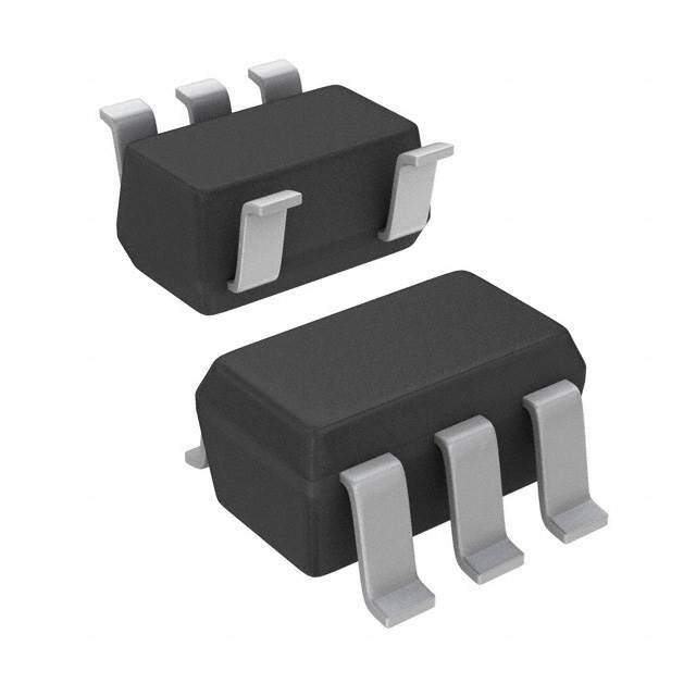
| 供应商器件封装 | SOT-23-5 |
| 其它名称 | 296-22156-1 |
| 制造商产品页 | http://www.ti.com/general/docs/suppproductinfo.tsp?distId=10&orderablePartNumber=INA195AQDBVRQ1 |
| 功能 | 电流监控器 |
| 包装 | 剪切带 (CT) |
| 安装类型 | 表面贴装 |
| 封装/外壳 | SC-74A,SOT-753 |
| 工作温度 | -55°C ~ 125°C |
| 感应方法 | 高端 |
| 标准包装 | 1 |
| 电压-输入 | -16 V ~ 80 V |
| 电流-输出 | - |
| 精度 | ±1% |


- 商务部:美国ITC正式对集成电路等产品启动337调查
- 曝三星4nm工艺存在良率问题 高通将骁龙8 Gen1或转产台积电
- 太阳诱电将投资9.5亿元在常州建新厂生产MLCC 预计2023年完工
- 英特尔发布欧洲新工厂建设计划 深化IDM 2.0 战略
- 台积电先进制程称霸业界 有大客户加持明年业绩稳了
- 达到5530亿美元!SIA预计今年全球半导体销售额将创下新高
- 英特尔拟将自动驾驶子公司Mobileye上市 估值或超500亿美元
- 三星加码芯片和SET,合并消费电子和移动部门,撤换高东真等 CEO
- 三星电子宣布重大人事变动 还合并消费电子和移动部门
- 海关总署:前11个月进口集成电路产品价值2.52万亿元 增长14.8%


PDF Datasheet 数据手册内容提取
Product Order Technical Tools & Support & Folder Now Documents Software Community INA193A-Q1,INA194A-Q1,INA195A-Q1 INA196A-Q1,INA197A-Q1,INA198A-Q1 SBOS366D–AUGUST2006–REVISEDJULY2015 INA19xA-Q1 Current Shunt Monitors –16-V to 80-V Common-Mode Range 1 Features 3 Description • QualifiedforAutomotiveApplications The INA19xA-Q1 family of current shunt monitors 1 with voltage output can sense drops across shunts at • WideCommon-ModeVoltage: common-mode voltages from –16 V to 80 V, –16Vto80V independent of the INA19xA supply voltage. They are • LowError:3%Overtemperature(Maximum) available with three output voltage scales: 20 V/V, • Bandwidth:Upto500kHz 50 V/V, and 100 V/V. The 500-kHz bandwidth simplifies use in current control loops and monitoring • ThreeTransferFunctionsAvailable: DC motor health. The INA193A–INA195A provide 20V/V,50V/V,and100V/V identical functions but alternative pin configurations to • CompleteCurrent-SenseSolution theINA196A–INA198A,respectively. The INA19xA-Q1 operate from a single 2.7-V to 18-V 2 Applications supply. They are specified over the extended • WeldingEquipment operating temperature range (–40°C to 125°C), and areofferedinaspace-savingSOT-23package. • BodyControlModules • LoadHealthMonitoring DeviceInformation(1) • TelecomEquipment PARTNUMBER PACKAGE BODYSIZE(NOM) • HEV/EVPowertrain INA19xA-Q1 SOT-23(5) 2.90mm×1.60mm • PowerManagement (1) Forallavailablepackages,seethepackageoptionaddendum • BatteryChargers attheendofthedatasheet. SimplifiedSchematic R I S S V IN+ –16V to +80V V+ 2.7V to 18V Negative VIN+ VIN– Load and Positive 5 kΩ 5 kΩ Common-Mode Voltage A1 A2 IRR OUT = S5 kSΩL R L INA193A–INA198A 1 An IMPORTANT NOTICE at the end of this data sheet addresses availability, warranty, changes, use in safety-critical applications, intellectualpropertymattersandotherimportantdisclaimers.PRODUCTIONDATA.
INA193A-Q1,INA194A-Q1,INA195A-Q1 INA196A-Q1,INA197A-Q1,INA198A-Q1 SBOS366D–AUGUST2006–REVISEDJULY2015 www.ti.com Table of Contents 1 Features.................................................................. 1 7.4 DeviceFunctionalModes........................................16 2 Applications........................................................... 1 8 ApplicationandImplementation........................ 20 3 Description............................................................. 1 8.1 ApplicationInformation............................................20 4 RevisionHistory..................................................... 2 8.2 TypicalApplication .................................................20 5 PinConfigurationandFunctions......................... 3 9 PowerSupplyRecommendations...................... 21 6 Specifications......................................................... 4 10 Layout................................................................... 22 6.1 AbsoluteMaximumRatings......................................4 10.1 LayoutGuidelines.................................................22 6.2 ESDRatings..............................................................4 10.2 LayoutExample....................................................22 6.3 RecommendedOperatingConditions.......................4 11 DeviceandDocumentationSupport................. 23 6.4 ThermalInformation..................................................4 11.1 RelatedLinks........................................................23 6.5 ElectricalCharacteristics...........................................5 11.2 ReceivingNotificationofDocumentationUpdates23 6.6 TypicalCharacteristics..............................................7 11.3 CommunityResources..........................................23 7 DetailedDescription............................................ 11 11.4 Trademarks...........................................................23 7.1 Overview.................................................................11 11.5 ElectrostaticDischargeCaution............................23 7.2 FunctionalBlockDiagram.......................................11 11.6 Glossary................................................................23 7.3 FeatureDescription.................................................11 12 Mechanical,Packaging,andOrderable Information........................................................... 23 4 Revision History NOTE:Pagenumbersforpreviousrevisionsmaydifferfrompagenumbersinthecurrentversion. ChangesfromRevisionC(October2008)toRevisionD Page • AddedESDRatingstable,FeatureDescriptionsection,DeviceFunctionalModes,ApplicationandImplementation section,PowerSupplyRecommendationssection,Layoutsection,DeviceandDocumentationSupportsection,and Mechanical,Packaging,andOrderableInformationsection ................................................................................................. 1 • AddedInputBiasCurrentvsCommonModeVoltageVs=5VgraphtoTypicalCharacteristics............................................. 7 • AddedInputBiasCurrentvsCommonModeVoltageVs=12VgraphtoTypicalCharacteristics......................................... 7 2 SubmitDocumentationFeedback Copyright©2006–2015,TexasInstrumentsIncorporated ProductFolderLinks:INA193A-Q1 INA194A-Q1 INA195A-Q1INA196A-Q1 INA197A-Q1 INA198A-Q1
INA193A-Q1,INA194A-Q1,INA195A-Q1 INA196A-Q1,INA197A-Q1,INA198A-Q1 www.ti.com SBOS366D–AUGUST2006–REVISEDJULY2015 5 Pin Configuration and Functions DBVPackage 5-PinSOT-23 DBVPackage INA193A-Q1,INA194A-Q1,INA195A-Q1TopView 5-PinSOT-23 INA196A-Q1,INA197A-Q1,INA198A-Q1TopView OUT 1 5 V+ OUT 1 5 V IN- GND 2 GND 2 V 3 4 V IN+ IN- V+ 3 4 V IN+ PinFunctions PIN INA193A-Q1, INA196A-Q1, TYPE DESCRIPTION NAME INA194A-Q1, INA197A-Q1, INA195A-Q1 INA198A-Q1 GND 2 2 GND Ground OUT 1 1 O Outputvoltage V+ 5 3 Analog Powersupply,2.7to18V V 3 4 I Connecttosupplysideofshuntresistor IN+ V 4 5 I Connecttoloadsideofshuntresistor IN– Copyright©2006–2015,TexasInstrumentsIncorporated SubmitDocumentationFeedback 3 ProductFolderLinks:INA193A-Q1 INA194A-Q1 INA195A-Q1INA196A-Q1 INA197A-Q1 INA198A-Q1
INA193A-Q1,INA194A-Q1,INA195A-Q1 INA196A-Q1,INA197A-Q1,INA198A-Q1 SBOS366D–AUGUST2006–REVISEDJULY2015 www.ti.com 6 Specifications 6.1 Absolute Maximum Ratings overoperatingfree-airtemperaturerange(unlessotherwisenoted)(1) MIN MAX UNIT Supplyvoltage 18 V Differentialinputvoltagerange,analoginputs(V –V ) –18 18 V IN+ IN– Common-modevoltagerange(2) –16 80 V Analogoutputvoltagerange(2) OUT GND–0.3 (V+)+0.3 V Inputcurrentintoanypin(2) 5 mA Junctiontemperature 150 °C Storagetemperature,T –65 150 °C stg (1) StressesbeyondthoselistedunderAbsoluteMaximumRatingsmaycausepermanentdamagetothedevice.Thesearestressratings only,whichdonotimplyfunctionaloperationofthedeviceattheseoranyotherconditionsbeyondthoseindicatedunderRecommended OperatingConditions.Exposuretoabsolute-maximum-ratedconditionsforextendedperiodsmayaffectdevicereliability. (2) Inputvoltageatanypinmayexceedthevoltageshownifthecurrentatthatpinislimitedto5mA. 6.2 ESD Ratings VALUE UNIT Human-bodymodel(HBM),perAECQ100-002(1) ±4000 V Electrostaticdischarge Charged-devicemodel(CDM),perAECQ100-011 ±1000 V (ESD) Machinemodel ±200 (1) AECQ100-002indicatesthatHBMstressingshallbeinaccordancewiththeANSI/ESDA/JEDECJS-001specification. 6.3 Recommended Operating Conditions overoperatingfree-airtemperaturerange(unlessotherwisenoted) MIN NOM MAX UNIT V Common-modeinputvoltage 12 V CM V+ Operatingsupplyvoltage 12 V T Operatingfree-airtemperature -40 125 ºC A 6.4 Thermal Information INA19xA-Q1 THERMALMETRIC(1) DBV(SOT-23) UNIT 5PINS R Junction-to-ambientthermalresistance 221.7 °C/W θJA R Junction-to-case(top)thermalresistance 144.7 °C/W θJC(top) R Junction-to-boardthermalresistance 49.7 °C/W θJB ψ Junction-to-topcharacterizationparameter 26.1 °C/W JT ψ Junction-to-boardcharacterizationparameter 49 °C/W JB (1) Formoreinformationabouttraditionalandnewthermalmetrics,seetheSemiconductorandICPackageThermalMetricsapplication report,SPRA953. 4 SubmitDocumentationFeedback Copyright©2006–2015,TexasInstrumentsIncorporated ProductFolderLinks:INA193A-Q1 INA194A-Q1 INA195A-Q1INA196A-Q1 INA197A-Q1 INA198A-Q1
INA193A-Q1,INA194A-Q1,INA195A-Q1 INA196A-Q1,INA197A-Q1,INA198A-Q1 www.ti.com SBOS366D–AUGUST2006–REVISEDJULY2015 6.5 Electrical Characteristics V =12V,V =12V,V =100mV(unlessotherwisenoted)FullrangeT =–40°Cto125°C S IN+ SENSE A PARAMETER TESTCONDITIONS T MIN TYP MAX UNIT A INPUT (V –0.2)/ V Full-scaleinputvoltage V =V −V 25°C 0.15 S V SENSE SENSE IN+ IN– Gain VCM Common-modeinput Fullrange –16 80 V V =−16Vto80V 25°C 80 94 IN+ CMR Common-moderejection dB V =12Vto80V Fullrange 100 120 IN+ 25°C ±0.5 2 V Offsetvoltage,RTI mV OS Fullrange 0.5 3 dV /dT Offsetvoltagevstemperature Fullrange 2.5 μV/°C OS Offsetvoltagevs V =2.7Vto18V, PSR S Fullrange 5 100 μV/V powersupply V =18V IN+ I Inputbiascurrent V pin Fullrange ±8 ±23 μA B IN– OUTPUT(V ≥20mV) SENSE INA193A,INA196A 20 G Gain INA194A,INA197A 25°C 50 V/V INA195A,INA198A 100 25°C ±0.2% ±1% Gainerror V =20mVto100mV SENSE Fullrange ±2% 25°C ±0.75% ±2.2% Totaloutputerror(1) Fullrange ±1% ±3% Nonlinearityerror V =20mVto100mV 25°C ±0.002% ±0.1% SENSE R Outputimpedance 25°C 1.5 Ω O Maximumcapacitiveload Nosustainedoscillation 25°C 10 nF OUTPUT(V <20mV) (2) SENSE –16V≤V <0 300 CM Alldevices mV V <V ≤80V 300 S CM INA193A, 0.4 INA196A V Outputvoltage 25°C OUT INA194A, 0V≤V ≤V , CM S 1 V INA197A V =5V S INA195A, 2 INA198A VOLTAGEOUTPUT(3) SwingtoV+power-supplyrail R =100kΩtoGND Fullrange V+–0.1 V+–0.2 V L SwingtoGND(4) R =100kΩtoGND Fullrange V +3 V +50 mV L GND GND (1) TotaloutputerrorincludeseffectsofgainerrorandV . OS (2) Fordetailsonthisregionofoperation,seeAccuracyVariationsasaResultOfV andCommonModeVoltage. SENSE (3) SeeFigure7. (4) Specifiedbydesign Copyright©2006–2015,TexasInstrumentsIncorporated SubmitDocumentationFeedback 5 ProductFolderLinks:INA193A-Q1 INA194A-Q1 INA195A-Q1INA196A-Q1 INA197A-Q1 INA198A-Q1
INA193A-Q1,INA194A-Q1,INA195A-Q1 INA196A-Q1,INA197A-Q1,INA198A-Q1 SBOS366D–AUGUST2006–REVISEDJULY2015 www.ti.com Electrical Characteristics (continued) V =12V,V =12V,V =100mV(unlessotherwisenoted)FullrangeT =–40°Cto125°C S IN+ SENSE A PARAMETER TESTCONDITIONS T MIN TYP MAX UNIT A FREQUENCYRESPONSE INA193A, 500 INA196A INA194A, BW Bandwidth C =5pF 25°C 300 kHz INA197A LOAD INA195A, 200 INA198A Phasemargin C <10nF 25°C 40 ° LOAD SR Slewrate 1 V/μs V =10mVto100mV , t Settlingtime(1%) SENSE PP 25°C 2 μs s C =5pF LOAD NOISE,RTI Voltagenoisedensity 25°C 40 nV/√Hz POWERSUPPLY V Operatingvoltage Fullrange 2.7 18 V S V =2V Fullrange 700 1250 OUT INA193A, INA194A, 370 950 I Quiescentcurrent INA196A, μA Q INA197A VSENSE=0mV Fullrange INA195A, 370 1050 INA198A TEMPERATURERANGE Operatingtemperature –40 125 °C Storagetemperature –65 150 °C 6 SubmitDocumentationFeedback Copyright©2006–2015,TexasInstrumentsIncorporated ProductFolderLinks:INA193A-Q1 INA194A-Q1 INA195A-Q1INA196A-Q1 INA197A-Q1 INA198A-Q1
INA193A-Q1,INA194A-Q1,INA195A-Q1 INA196A-Q1,INA197A-Q1,INA198A-Q1 www.ti.com SBOS366D–AUGUST2006–REVISEDJULY2015 6.6 Typical Characteristics T =25°C,V =12V,V =12V,andV =100mV(unlessotherwisenoted) A S IN+ SENSE 45 45 G=100 CLOAD=1000 pF G=100 40 40 G=50 G=50 35 35 30 30 B) G=20 B) G=20 d d ( 25 ( 25 n n ai ai G 20 G 20 15 15 10 10 5 5 10k 100k 1M 10k 100k 1M Frequency(Hz) Frequency(Hz) Figure1.GainvsFrequency Figure2.GainvsFrequency 20 140 18 130 100V/V 16 B) 120 CMR d ( V) 1142 50V/V odeandejection 111000 V(OUT 108 20V/V mon-MupplyR 9800 PSR 6 Comer-S 70 4 w 60 o P 2 50 0 40 20 100 200 300 400 500 600 700 800 900 10 100 1k 10k 100k V (mV) Frequency(Hz) DIFFERENTIAL Figure3.GainPlot Figure4.Common-ModeandPower-SupplyRejectionvs Frequency 4.0 0.1 e) 3.5 0.09 u al 0.08 v 3.0 Erroraloutput 2.5 or (%) 00..0076 utde 2.0 Err 0.05 Outpofthei 1.5 Output 00..0043 or 1.0 err 0.02 % 0.5 ( 0.01 0 0 0 50 100 150 200 250 300 350 400 450 500 –16–12 –8 –4 0 4 8 12 16 20 ... 76 80 VSENSE(mV) Common-ModeVoltage (V) Figure5.OutputErrorvsVsense Figure6.OutputErrorvsCommon-ModeVoltage Copyright©2006–2015,TexasInstrumentsIncorporated SubmitDocumentationFeedback 7 ProductFolderLinks:INA193A-Q1 INA194A-Q1 INA195A-Q1INA196A-Q1 INA197A-Q1 INA198A-Q1
INA193A-Q1,INA194A-Q1,INA195A-Q1 INA196A-Q1,INA197A-Q1,INA198A-Q1 SBOS366D–AUGUST2006–REVISEDJULY2015 www.ti.com Typical Characteristics (continued) T =25°C,V =12V,V =12V,andV =100mV(unlessotherwisenoted) A S IN+ SENSE 12 1000 11 V = 12V 900 10 SSourcing Current 800 9 V) 8 25°C 700 ge ( 7 125°C –40°C 600 utVolta 65 VSSou=r c3inVg Current I(µA)Q 540000 Outp 4 25°C –40°C Output stage is designed 300 3 to source current.Current 200 2 sinking capability is 1 approximately 400 µA. 100 125°C 0 0 0 5 10 15 20 25 30 0 1 2 3 4 5 6 7 8 9 10 Output Current (mA) OutputVoltage (V) Figure7.PositiveOutputVoltageSwingvsOutputCurrent Figure8.QuiescentCurrentvsOutputVoltage 15 15 12.5 IN- 12.5 10 10 Current (A)P 27..555 IN+ Current (A)P 27..555 as 0 as 0 ut Bi -2.5 ut Bi -2.5 np -5 np -5 I I -7.5 -7.5 IN+ -10 -10 IN- -12.5 -12.5 -20 -10 0 10 20 30 40 50 60 70 80 -20 -10 0 10 20 30 40 50 60 70 80 Common-Mode Voltage (V) Common-Mode Voltage (V) D001 D102 Vs=5V Vs=12V Figure9.InputBiasCurrentvsCommonModeVoltage Figure10.InputBiasCurrentvsCommonModeVoltage 875 34 V = 100 mV –40°C SENSE V = 12V V = 2.7V 775 S S A) 30 m 25°C 675 urrent ( 26 125°C A) 575 uit C 22 µ c I(Q 475 VS= 12V ort-Cir 18 375 Sh 14 VSENSE= 0 mV VS= 2.7V ut 275 utp 10 O 175 6 –16–12 –8 –4 0 4 8 12 16 20 ... 76 80 2.5 3.5 4.5 5.5 6.5 7.5 8.5 9.5 10.5 11.5 17 18 V (V) SupplyVoltage (V) CM Figure11.QuiescentCurrentvsCommonModeVoltage Figure12.OutputShortCircuitCurrentvsSupplyVoltage 8 SubmitDocumentationFeedback Copyright©2006–2015,TexasInstrumentsIncorporated ProductFolderLinks:INA193A-Q1 INA194A-Q1 INA195A-Q1INA196A-Q1 INA197A-Q1 INA198A-Q1
INA193A-Q1,INA194A-Q1,INA195A-Q1 INA196A-Q1,INA197A-Q1,INA198A-Q1 www.ti.com SBOS366D–AUGUST2006–REVISEDJULY2015 Typical Characteristics (continued) T =25°C,V =12V,V =12V,andV =100mV(unlessotherwisenoted) A S IN+ SENSE G=20 G=20 mV/div) mV/div) Voltage (50 Voltage (500 Output Output V = 10 mV to 20 mV V = 10 mV to 100 mV SENSE SENSE Time (2 µs/div) Time (2 µs/div) Figure13.StepResponse Figure14.StepResponse G=20 G=50 mV/div) mV/div) Voltage (50 Voltage (100 Output Output V = 90 mV to 100 mV V = 10 mV to 20 mV SENSE SENSE Time (2 µs/div) Time (5 µs/div) Figure15.StepResponse Figure16.StepResponse G=50 G=50 v) div) V/di V/ m oltage (1 age (100 utV Volt Outp utput O V = 10 mV to 100 mV V = 90 mV to 100 mV SENSE SENSE Time (5 µs/div) Time (5 µs/div) Figure17.StepResponse Figure18.StepResponse Copyright©2006–2015,TexasInstrumentsIncorporated SubmitDocumentationFeedback 9 ProductFolderLinks:INA193A-Q1 INA194A-Q1 INA195A-Q1INA196A-Q1 INA197A-Q1 INA198A-Q1
INA193A-Q1,INA194A-Q1,INA195A-Q1 INA196A-Q1,INA197A-Q1,INA198A-Q1 SBOS366D–AUGUST2006–REVISEDJULY2015 www.ti.com Typical Characteristics (continued) T =25°C,V =12V,V =12V,andV =100mV(unlessotherwisenoted) A S IN+ SENSE G=100 v) di V/ 2 ( e g a olt V ut p ut O V = 10 mV to 100 mV SENSE Time (10 µs/div) Figure19.StepResponse 10 SubmitDocumentationFeedback Copyright©2006–2015,TexasInstrumentsIncorporated ProductFolderLinks:INA193A-Q1 INA194A-Q1 INA195A-Q1INA196A-Q1 INA197A-Q1 INA198A-Q1
INA193A-Q1,INA194A-Q1,INA195A-Q1 INA196A-Q1,INA197A-Q1,INA198A-Q1 www.ti.com SBOS366D–AUGUST2006–REVISEDJULY2015 7 Detailed Description 7.1 Overview The INA193A−INA198A family of current shunt monitors with voltage output can sense drops across shunts at common mode voltages from −16 V to 80 V, independent of the INA19x supply voltage. They are available with three output voltage scales: 20 V/V, 50 V/V, and 100 V/V. The 500-kHz bandwidth simplifies use in current control loops. The INA193A−INA195A devices provide identical functions but alternative pin configurations to the INA196A−INA198A,respectively. The INA193A−INA198A devices operate from a single 2.7-V to 18-V supply, drawing a maximum of 900 μA of supply current. They are specified over the extended operating temperature range (−40°C to 125°C), and are offeredinaspace-savingSOT-23package. 7.2 Functional Block Diagram V V V+ IN+ R (1) IN(cid:16) R (1) 1 1 5 k: 5 k: A1 A2 G = 20, R = 100 k: OUT L G = 50, R = 250 k: L G = 100, R = 500 k: L R (1) L INA193A-INA198A GND 7.3 Feature Description 7.3.1 BasicConnection Figure 20 shows the basic connection of the INA19xA. The input pins, V and V , should be connected as IN+ IN– closelyaspossibletotheshuntresistortominimizeanyresistanceinserieswiththeshuntresistance. Power-supply bypass capacitors are required for stability. Applications with noisy or high-impedance power supplies may require additional decoupling capacitors to reject power-supply noise. Connect bypass capacitors closetothedevicepins. Copyright©2006–2015,TexasInstrumentsIncorporated SubmitDocumentationFeedback 11 ProductFolderLinks:INA193A-Q1 INA194A-Q1 INA195A-Q1INA196A-Q1 INA197A-Q1 INA198A-Q1
INA193A-Q1,INA194A-Q1,INA195A-Q1 INA196A-Q1,INA197A-Q1,INA198A-Q1 SBOS366D–AUGUST2006–REVISEDJULY2015 www.ti.com Feature Description (continued) RS IS V IN+ –16V to +80V V+ 2.7V to 18V V V Load IN+ IN– 5 kΩ 5 kΩ OUT INA193A–INA198A Figure20. INA19xABasicConnections 7.3.2 SelectingR S The value chosen for the shunt resistor, R , depends on the application and is a compromise between small- S signalaccuracyandmaximumpermissiblevoltagelossinthemeasurementline.HighvaluesofR providebetter S accuracy at lower currents by minimizing the effects of offset, while low values of R minimize voltage loss in the S supply line. For most applications, best performance is attained with an R value that provides a full-scale shunt S voltagerangeof50mVto100mV.Maximuminputvoltageforaccuratemeasurementsis500mV. 7.3.3 InsidetheINA19xA The INA19xA uses a new, unique, internal circuit topology that provides common mode range extending from –16 V to 80 V while operating from a single power supply. The common mode rejection in a classic instrumentation amplifier approach is limited by the requirement for accurate resistor matching. By converting the induced input voltage to a current, the INA19xA provides common mode rejection that is no longer a function of closely matched resistor values, providing the enhanced performance necessary for such a wide common mode range. A simplified diagram (see Figure 20) shows the basic circuit function. When the common mode voltage is positive,amplifierA2isactive. The differential input voltage, V – V applied across R , is converted to a current through a 5-kΩ resistor. IN+ IN– S This current is converted back to a voltage through R , and then amplified by the output buffer amplifier. When L the common mode voltage is negative, amplifier A1 is active. The differential input voltage, V – V applied IN+ IN– across R , is converted to a current through a 5-kΩ resistor. This current is sourced from a precision current S mirror whose output is directed into R , converting the signal back into a voltage and amplified by the output L buffer amplifier. Patent-pending circuit architecture ensures smooth device operation, even during the transition periodwherebothamplifiersA1andA2areactive. 12 SubmitDocumentationFeedback Copyright©2006–2015,TexasInstrumentsIncorporated ProductFolderLinks:INA193A-Q1 INA194A-Q1 INA195A-Q1INA196A-Q1 INA197A-Q1 INA198A-Q1
INA193A-Q1,INA194A-Q1,INA195A-Q1 INA196A-Q1,INA197A-Q1,INA198A-Q1 www.ti.com SBOS366D–AUGUST2006–REVISEDJULY2015 Feature Description (continued) R SHUNT 12V LOAD I 1 5V V V V+ IN+ IN– 5 kΩ 5 kΩ V+ INA193A–INA198A OUT for 12-V common mode INA193A–INA198A 5 kΩ 5 kΩ GND OUT for –12-V common mode V V GND IN+ IN– R SHUNT –12V LOAD I 2 Figure21. MonitorBipolarOutputPower-SupplyCurrent Copyright©2006–2015,TexasInstrumentsIncorporated SubmitDocumentationFeedback 13 ProductFolderLinks:INA193A-Q1 INA194A-Q1 INA195A-Q1INA196A-Q1 INA197A-Q1 INA198A-Q1
INA193A-Q1,INA194A-Q1,INA195A-Q1 INA196A-Q1,INA197A-Q1,INA198A-Q1 SBOS366D–AUGUST2006–REVISEDJULY2015 www.ti.com Feature Description (continued) R SHUNT V LOAD SUPPLY 5V 5V VIN+ VIN– V+ VIN+ VIN– V+ 5 kΩ 5 kΩ 5 kΩ 5 kΩ 5V INA152 40 kΩ 40 kΩ OUT OUT INA193A– INA193A– INA198A INA198A VOUT 40 kΩ 40 kΩ 2.5V V REF Figure22. BidirectionalCurrentMonitoring Up to 80V R SHUNT 2.7V to 18V Solenoid VIN+ VIN– V+ 5 kΩ 5 kΩ OUT INA193A– INA198A Figure23. InductiveCurrentMonitorIncludingFlyback 14 SubmitDocumentationFeedback Copyright©2006–2015,TexasInstrumentsIncorporated ProductFolderLinks:INA193A-Q1 INA194A-Q1 INA195A-Q1INA196A-Q1 INA197A-Q1 INA198A-Q1
INA193A-Q1,INA194A-Q1,INA195A-Q1 INA196A-Q1,INA197A-Q1,INA198A-Q1 www.ti.com SBOS366D–AUGUST2006–REVISEDJULY2015 Feature Description (continued) VIN+ VIN– V+ 5 kΩ 5 kΩ For output signals > comparator trip point R 1 OUT INA193A– TLV3012 INA198A R2 REF 1.25V Internal Reference (a) INA19xA Output Adjusted byVoltage Divider V V V+ IN+ IN– 5 kΩ 5 kΩ OUT INA193A– TLV3012 INA198A REF 1.25V R1 Internal Reference Forusewith R 2 smalloutputsignals. (b) Comparator ReferenceVoltage Adjusted byVoltage Divider Figure24. INA19xAWithComparator 7.3.4 PowerSupply The input circuitry of the INA19xA can accurately measure beyond its power-supply voltage, V+. For example, the V+ power supply can be 5 V, whereas the load power-supply voltage is up to 80 V. The output voltage range oftheOUTterminal,however,islimitedbythevoltagesonthepower-supplypin. Copyright©2006–2015,TexasInstrumentsIncorporated SubmitDocumentationFeedback 15 ProductFolderLinks:INA193A-Q1 INA194A-Q1 INA195A-Q1INA196A-Q1 INA197A-Q1 INA198A-Q1
INA193A-Q1,INA194A-Q1,INA195A-Q1 INA196A-Q1,INA197A-Q1,INA198A-Q1 SBOS366D–AUGUST2006–REVISEDJULY2015 www.ti.com 7.4 Device Functional Modes 7.4.1 InputFiltering An obvious and straightforward location for filtering is at the output of the INA19xA series; however, this location negates the advantage of the low output impedance of the internal buffer. The only other option for filtering is at the input pins of the INA19xA, which is complicated by the internal 5-kΩ ± 30% input impedance (see Figure 25). Using the lowest possible resistor values minimizes both the initial shift in gain and effects of tolerance. The effectoninitialgainisgivenby: ( 5 kΩ ( Gain Error % = 100 – 100 × 5 kΩ+ R FILT (1) Total effect on gain error can be calculated by replacing the 5-kΩ term with 5 kΩ – 30% (or 3.5 kΩ) or 5 kΩ + 30% (or 6.5 kΩ). The tolerance extremes of R can also be inserted into the equation. If a pair of 100- FILT Ω 1% resistors are used on the inputs, the initial gain error is 1.96%. Worst-case tolerance conditions always occur at the lower excursion of the internal 5-kΩ resistor (3.5 kΩ), and the higher excursion of R , 3% in this FILT case. The specified accuracy of the INA19xA must then be combined in addition to these tolerances. While this discussion treats accuracy worst-case conditions by combining the extremes of the resistor values, it is appropriatetousegeometricmeanorrootsumsquarecalculationstototaltheeffectsofaccuracyvariations. R <<R SHUNT FILTER V LOAD SUPPLY R <100 R <100 FILTER FILTER f(cid:18)3dB CFILTER f(cid:18)3dB= 2π(2R 1 )C FILTER FILTER 5V VIN+ VIN– V+ 5 kΩ 5 kΩ OUT INA193A–INA198A Figure25. InputFilter(GainError=1.5%to –2.2%) 7.4.2 AccuracyVariationsasaResultOfV andCommonModeVoltage SENSE The accuracy of the INA19xA-Q1 current shunt monitors is a function of two main variables: V (V – V ) and common mode voltage, V , relative to the supply voltage, V . V is expressed as SENSE IN+ IN– CM S CM (V + V )/2; however, in practice, V is seen as the voltage at V because the voltage drop across V IN+ IN– CM IN+ SENSE isusuallysmall. 16 SubmitDocumentationFeedback Copyright©2006–2015,TexasInstrumentsIncorporated ProductFolderLinks:INA193A-Q1 INA194A-Q1 INA195A-Q1INA196A-Q1 INA197A-Q1 INA198A-Q1
INA193A-Q1,INA194A-Q1,INA195A-Q1 INA196A-Q1,INA197A-Q1,INA198A-Q1 www.ti.com SBOS366D–AUGUST2006–REVISEDJULY2015 Device Functional Modes (continued) Thissectionaddressestheaccuracyofthesespecificoperatingregions: NormalCase1: V ≥20mV,V ≥ V SENSE CM S NormalCase2: V ≥20mV,V < V SENSE CM S LowV Case1: V <20mV, –16V≤ V < 0 SENSE SENSE CM LowV Case2: V <20mV,0V≤ V ≤ V SENSE SENSE CM S LowV Case3: V <20mV,V <V ≤ 80V SENSE SENSE S CM 7.4.2.1 NormalCase1:V ≥20mV,V ≥ V SENSE CM S This region of operation provides the highest accuracy. Here, the input offset voltage is characterized and measuredusingatwo-stepmethod.First,thegainisdeterminedby(Equation2). V -V G= OUT1 OUT2 100mV-20mV where • V =OutputvoltagewithV =100mV OUT1 SENSE • V =OutputvoltagewithV =20mV (2) OUT2 SENSE The offset voltage is then measured at V = 100 mV and referred to the input (RTI) of the current shunt SENSE monitor,asshownin(Equation3). æVOUT1ö V RTI(Referred-To-Input)=ç ÷-100mV OS è G ø (3) In the Typical Characteristics, the Output Error vs Common Mode Voltage curve shows the highest accuracy for thethisregionofoperation.Inthisplot,V =12V;forV ≥12V,theoutputerrorisatitsminimum.Thiscaseis S CM alsousedtocreatetheV ≥20mVoutputspecificationsintheElectricalCharacteristics table. SENSE 7.4.2.2 NormalCase2:V ≥20mV,V < V SENSE CM S This region of operation has slightly less accuracy than Normal Case 1 as a result of the common mode operating area in which the part functions, as seen in Figure 6. As noted, for this graph V = 12 V; for V < 12 S CM V, the Output Error increases as V becomes less than 12 V, with a typical maximum error of 0.005% at the CM mostnegativeV =–16V. CM 7.4.2.3 LowV Case1:V <20mV, –16V ≤ V <0;andLowV Case3:V < 20mV, SENSE SENSE CM SENSE SENSE V <V ≤ 80V S CM Although the INA19xA-Q1 family of devices are not designed for accurate operation in either of these regions, some applications are exposed to these conditions; for example, when monitoring power supplies that are switched on and off while V is still applied to the INA19xA-Q1. It is important to know what the behavior of the S deviceswillbeintheseregions. As V approaches 0 mV, in these V regions, the device output accuracy degrades. A larger-than-normal SENSE CM offset can appear at the current shunt monitor output with a typical maximum value of V = 300 mV for OUT V = 0 mV. As V approaches 20 mV, V returns to the expected output value with accuracy as SENSE SENSE OUT specified in Electrical Characteristics. Figure 26 illustrates this effect using the INA195A and INA198A (Gain=100). Copyright©2006–2015,TexasInstrumentsIncorporated SubmitDocumentationFeedback 17 ProductFolderLinks:INA193A-Q1 INA194A-Q1 INA195A-Q1INA196A-Q1 INA197A-Q1 INA198A-Q1
INA193A-Q1,INA194A-Q1,INA195A-Q1 INA196A-Q1,INA197A-Q1,INA198A-Q1 SBOS366D–AUGUST2006–REVISEDJULY2015 www.ti.com Device Functional Modes (continued) 2.0 1.8 1.6 1.4 1.2 V) Actual (T 1.0 U O V 0.8 Ideal 0.6 0.4 0.2 0 0 2 4 6 8 10 12 14 16 18 20 V (mV) SENSE Figure26. ExampleforLowV Cases1and3 SENSE (INA195A-Q1,INA198A-Q1:Gain=100) 7.4.2.4 LowV Case2:V <20mV,0V ≤ V ≤ V SENSE SENSE CM S This region of operation is the least accurate for the INA19xA-Q1 family. To achieve the wide input common mode voltage range, these devices use two operational amplifier front ends in parallel. One operational amplifier front end operates in the positive input common mode voltage range, and the other in the negative input region. For this case, neither of these two internal amplifiers dominates and overall loop gain is very low. Within this region, V approaches voltages close to linear operation levels for Normal Case 2. This deviation from linear OUT operation becomes greatest the closer V approaches 0 V. Within this region, as V approaches 20 mV, SENSE SENSE device operation is closer to that described by Normal Case 2. Figure 27 illustrates this behavior for the INA195A. The V maximum peak for this case is tested by maintaining a constant V , setting V = 0 mV OUT S SENSE and sweeping V from 0 V to V . The exact V at which V peaks during this test varies from part to part, CM S CM OUT buttheV maximumpeakistestedtobelessthanthespecifiedV testedlimit. OUT OUT 2.4 INA195,INA198V TestedLimit(1) 2.2 OUT V 2.0 CM1 Ideal 1.8 V CM2 1.6 (V)T 11..42 VCM3 U VO 1.0 0.8 V CM4 0.6 0.4 0.2 0 0 2 4 6 8 10 12 14 16 18 20 22 24 V (mV) SENSE (1) INA193,INA196V TestedLimit=0.4V OUT INA194,INA197V TestedLimit=1V OUT NOTE: V testedlimitatV =0mV,0≤V ≤VS. OUT SENSE CM1 V ,V ,andV illustratethevariancefromparttopartoftheV thatcancausemaximumV withV CM2 CM3 CM4 CM OUT SENSE <20mV. Figure27. ExampleforLowV Case2 SENSE (INA195A,INA198A:Gain=100) 18 SubmitDocumentationFeedback Copyright©2006–2015,TexasInstrumentsIncorporated ProductFolderLinks:INA193A-Q1 INA194A-Q1 INA195A-Q1INA196A-Q1 INA197A-Q1 INA198A-Q1
INA193A-Q1,INA194A-Q1,INA195A-Q1 INA196A-Q1,INA197A-Q1,INA198A-Q1 www.ti.com SBOS366D–AUGUST2006–REVISEDJULY2015 Device Functional Modes (continued) 7.4.3 Shutdown Because the INA19xA-Q1 consume a quiescent current less than 1 mA, they can be powered by either the output of logic gates or by transistor switches to supply power. Use a totem pole output buffer or gate that can provide sufficient drive along with 0.1 μF bypass capacitor, preferably ceramic with good high frequency characteristics. This gate should have a supply voltage of 3 V or greater because the INA19xA-Q1 requires a minimum supply greater than 2.7 V. In addition to eliminating quiescent current, this gate also turns off the 10 μA biascurrentpresentateachoftheinputs.AnexampleshutdowncircuitisshowninFigure28. RS IL V IN+ -16 V to 80 V Negative VIN+ VIN- V+ Load and Positive R R 1 2 Common-Mode Voltage V+>3 V A1 0.1mF A2 OUT R L INA193A-INA198A Figure28. INA19xA-Q1ExampleShutdownCircuit 7.4.4 TransientProtection The –16-V to 80-V common mode range of the INA19xA is ideal for withstanding automotive fault conditions ranging from 12-V battery reversal up to 80-V transients, because no additional protective components are needed up to those levels. In the event that the INA19xA is exposed to transients on the inputs in excess of its ratings, then external transient absorption with semiconductor transient absorbers (zeners or Transzorbs) are necessary. TI does not recommend using MOVs or VDRs except when they are used in addition to a semiconductor transient absorber. Select the transient absorber such that it never allows the INA19xA to be exposed to transients greater than 80 V (that is, allow for transient absorber tolerance, as well as additional voltage due to transient absorber dynamic impedance). Despite the use of internal zener-type ESD protection, the INA19xA does not lend itself to using external resistors in series with the inputs because the internal gain resistors can vary up to ±30%. (If gain accuracy is not important, then resistors can be added in series with the INA19xAinputswithtwoequalresistorsoneachinput.) 7.4.5 OutputVoltageRange The output of the INA19xA is accurate within the output voltage swing range set by the power supply pin, V+. ThisisbestillustratedwhenusingtheINA195AorINA198A(whicharebothversionsusingagainof100),where a 100-mV full-scale input from the shunt resistor requires an output voltage swing of 10 V, and a power-supply voltagesufficienttoachieve10Vontheoutput. Copyright©2006–2015,TexasInstrumentsIncorporated SubmitDocumentationFeedback 19 ProductFolderLinks:INA193A-Q1 INA194A-Q1 INA195A-Q1INA196A-Q1 INA197A-Q1 INA198A-Q1
INA193A-Q1,INA194A-Q1,INA195A-Q1 INA196A-Q1,INA197A-Q1,INA198A-Q1 SBOS366D–AUGUST2006–REVISEDJULY2015 www.ti.com 8 Application and Implementation NOTE Information in the following applications sections is not part of the TI component specification, and TI does not warrant its accuracy or completeness. TI’s customers are responsible for determining suitability of components for their purposes. Customers should validateandtesttheirdesignimplementationtoconfirmsystemfunctionality. 8.1 Application Information The INA193A-INA198A devices measure the voltage developed across a current-sensing resistor when current passes through it. The ability to have shunt common mode voltages from −16-V to 80-V drive and control the outputsignalwithVsoffersmultipleconfigurations,asdiscussedthroughoutthissection. 8.2 Typical Application The device is a unidirectional, current-sense amplifier capable of measuring currents through a resistive shunt with shunt common mode voltages from −16 V to 80 V. Two devices can be configured for bidirectional monitoring and is common in applications that include charging and discharging operations where the current flow-throughresistorcanchangedirections. R SHUNT V LOAD SUPPLY 5V 5V VIN+ VIN– V+ VIN+ VIN– V+ 5 kΩ 5 kΩ 5 kΩ 5 kΩ 5V INA152 40 kΩ 40 kΩ OUT OUT INA193A– INA193A– INA198A INA198A VOUT 40 kΩ 40 kΩ 2.5V V REF Figure29. BidirectionalCurrentMonitoring 8.2.1 DesignRequirements Vsupply is set to 12 V, Vref at 2.5 V and a 10-mΩ shunt. The accuracy of the current will typically be less than 0.5% for current greater than ±2 A. For current lower than ±2 A, the accuracy will vary; use the Accuracy VariationsasaResultOfV andCommonModeVoltagesectionforaccuracyconsiderations. SENSE 20 SubmitDocumentationFeedback Copyright©2006–2015,TexasInstrumentsIncorporated ProductFolderLinks:INA193A-Q1 INA194A-Q1 INA195A-Q1INA196A-Q1 INA197A-Q1 INA198A-Q1
INA193A-Q1,INA194A-Q1,INA195A-Q1 INA196A-Q1,INA197A-Q1,INA198A-Q1 www.ti.com SBOS366D–AUGUST2006–REVISEDJULY2015 Typical Application (continued) 8.2.2 DetailedDesignProcedure The ability to measure this current flowing in both directions is enabled by adding a unity gain amplifier with a V ,asshowninFigure29.TheoutputthenrespondsbyincreasingaboveVREFforpositivedifferentialsignals REF (relative to the IN – pin) and responds by decreasing below VREF for negative differential signals. This reference voltage applied to the REF pin can be set anywhere from 0 V to V+. For bidirectional applications, VREF is typically set at mid- scale for equal signal range in both current directions. In some cases, however, VREF is set at a voltage other than mid-scale when the bidirectional current and corresponding output signal are not required tobesymmetrical. 8.2.3 ApplicationCurve An example output response of a bidirectional configuration is shown in Figure 30. With the REF pin connected to a reference voltage, 2.5 V in this case, the output voltage is biased upwards by this reference level. The output rises above the reference voltage for positive differential input signals and falls below the reference voltagefornegativedifferentialinputsignals. 10 I_in 7.5 VOUT V) 5 ge ( 2.5 a olt V 0 (I), ent -2.5 urr C -5 -7.5 -10 0 2 4 6 8 10 12 14 16 18 20 Time (µs) Figure30.OutputVoltagevsShuntInputCurrent 9 Power Supply Recommendations The input circuitry of the INA193A-INA198A devices can accurately measure beyond its power-supply voltage, V+. For example, the V+ power supply can be 5 V, whereas the load power-supply voltage is up to 80 V. The outputvoltagerangeoftheOUTterminal,however,islimitedbythevoltagesonthepower-supplypin. Copyright©2006–2015,TexasInstrumentsIncorporated SubmitDocumentationFeedback 21 ProductFolderLinks:INA193A-Q1 INA194A-Q1 INA195A-Q1INA196A-Q1 INA197A-Q1 INA198A-Q1
INA193A-Q1,INA194A-Q1,INA195A-Q1 INA196A-Q1,INA197A-Q1,INA198A-Q1 SBOS366D–AUGUST2006–REVISEDJULY2015 www.ti.com 10 Layout 10.1 Layout Guidelines 10.1.1 RFI/EMI TI always recommends adhering to good layout practices. Keep traces short and, when possible, use a printed- circuit-board (PCB) ground plane with surface-mount components placed as close to the device pins as possible. Small ceramic capacitors placed directly across amplifier inputs can reduce RFI/EMI sensitivity. PCB layout should locate the amplifier as far away as possible from RFI sources. Sources can include other components in thesamesystemastheamplifieritself,suchasinductors(particularlyswitchedinductorshandlingalotofcurrent and at high frequencies). RFI can generally be identified as a variation in offset voltage or dc signal levels with changes in the interfering RF signal. If the amplifier cannot be located away from sources of radiation, shielding may be needed. Twisting wire input leads makes them more resistant to RF fields. The difference in input pin locationoftheINA193A–INA195AversustheINA196A–INA198AmayprovidedifferentEMIperformance. 10.2 Layout Example Via to Power or Ground Plane Via to Internal Layer Supply Bypass Capacitor Output Signal Supply Voltage OUT V+ GND IN+ IN- Shunt Resistor Figure31. RecommendedLayout 22 SubmitDocumentationFeedback Copyright©2006–2015,TexasInstrumentsIncorporated ProductFolderLinks:INA193A-Q1 INA194A-Q1 INA195A-Q1INA196A-Q1 INA197A-Q1 INA198A-Q1
INA193A-Q1,INA194A-Q1,INA195A-Q1 INA196A-Q1,INA197A-Q1,INA198A-Q1 www.ti.com SBOS366D–AUGUST2006–REVISEDJULY2015 11 Device and Documentation Support 11.1 Related Links Table 1 lists quick access links. Categories include technical documents, support and community resources, toolsandsoftware,andquickaccesstosampleorbuy. Table1.RelatedLinks TECHNICAL TOOLS& SUPPORT& PARTS PRODUCTFOLDER SAMPLE&BUY DOCUMENTS SOFTWARE COMMUNITY INA193A-Q1 Clickhere Clickhere Clickhere Clickhere Clickhere INA194A-Q1 Clickhere Clickhere Clickhere Clickhere Clickhere INA195A-Q1 Clickhere Clickhere Clickhere Clickhere Clickhere INA196A-Q1 Clickhere Clickhere Clickhere Clickhere Clickhere INA197A-Q1 Clickhere Clickhere Clickhere Clickhere Clickhere INA198A-Q1 Clickhere Clickhere Clickhere Clickhere Clickhere 11.2 Receiving Notification of Documentation Updates To receive notification of documentation updates, navigate to the device product folder on ti.com. In the upper right corner, click on Alert me to register and receive a weekly digest of any product information that has changed.Forchangedetails,reviewtherevisionhistoryincludedinanyreviseddocument. 11.3 Community Resources The following links connect to TI community resources. Linked contents are provided "AS IS" by the respective contributors. They do not constitute TI specifications and do not necessarily reflect TI's views; see TI's Terms of Use. TIE2E™OnlineCommunity TI'sEngineer-to-Engineer(E2E)Community.Createdtofostercollaboration amongengineers.Ate2e.ti.com,youcanaskquestions,shareknowledge,exploreideasandhelp solveproblemswithfellowengineers. DesignSupport TI'sDesignSupport QuicklyfindhelpfulE2Eforumsalongwithdesignsupporttoolsand contactinformationfortechnicalsupport. 11.4 Trademarks E2EisatrademarkofTexasInstruments. Allothertrademarksarethepropertyoftheirrespectiveowners. 11.5 Electrostatic Discharge Caution Thesedeviceshavelimitedbuilt-inESDprotection.Theleadsshouldbeshortedtogetherorthedeviceplacedinconductivefoam duringstorageorhandlingtopreventelectrostaticdamagetotheMOSgates. 11.6 Glossary SLYZ022—TIGlossary. Thisglossarylistsandexplainsterms,acronyms,anddefinitions. 12 Mechanical, Packaging, and Orderable Information The following pages include mechanical, packaging, and orderable information. This information is the most current data available for the designated devices. This data is subject to change without notice and revision of thisdocument.Forbrowser-basedversionsofthisdatasheet,refertotheleft-handnavigation. Copyright©2006–2015,TexasInstrumentsIncorporated SubmitDocumentationFeedback 23 ProductFolderLinks:INA193A-Q1 INA194A-Q1 INA195A-Q1INA196A-Q1 INA197A-Q1 INA198A-Q1
PACKAGE OPTION ADDENDUM www.ti.com 6-Feb-2020 PACKAGING INFORMATION Orderable Device Status Package Type Package Pins Package Eco Plan Lead/Ball Finish MSL Peak Temp Op Temp (°C) Device Marking Samples (1) Drawing Qty (2) (6) (3) (4/5) INA193AQDBVRQ1 ACTIVE SOT-23 DBV 5 3000 Green (RoHS NIPDAU Level-2-260C-1 YEAR -40 to 125 BOG & no Sb/Br) INA194AQDBVRQ1 ACTIVE SOT-23 DBV 5 3000 Green (RoHS NIPDAU Level-2-260C-1 YEAR -40 to 125 BOH & no Sb/Br) INA195AQDBVRQ1 ACTIVE SOT-23 DBV 5 3000 Green (RoHS NIPDAU Level-2-260C-1 YEAR -40 to 125 BOI & no Sb/Br) INA196AQDBVRQ1 ACTIVE SOT-23 DBV 5 3000 Green (RoHS NIPDAU Level-2-260C-1 YEAR -40 to 125 BOJ & no Sb/Br) INA197AQDBVRQ1 ACTIVE SOT-23 DBV 5 3000 Green (RoHS NIPDAU Level-2-260C-1 YEAR -40 to 125 BOK & no Sb/Br) INA198AQDBVRQ1 ACTIVE SOT-23 DBV 5 3000 Green (RoHS NIPDAU Level-2-260C-1 YEAR -40 to 125 BOL & no Sb/Br) (1) The marketing status values are defined as follows: ACTIVE: Product device recommended for new designs. LIFEBUY: TI has announced that the device will be discontinued, and a lifetime-buy period is in effect. NRND: Not recommended for new designs. Device is in production to support existing customers, but TI does not recommend using this part in a new design. PREVIEW: Device has been announced but is not in production. Samples may or may not be available. OBSOLETE: TI has discontinued the production of the device. (2) RoHS: TI defines "RoHS" to mean semiconductor products that are compliant with the current EU RoHS requirements for all 10 RoHS substances, including the requirement that RoHS substance do not exceed 0.1% by weight in homogeneous materials. Where designed to be soldered at high temperatures, "RoHS" products are suitable for use in specified lead-free processes. TI may reference these types of products as "Pb-Free". RoHS Exempt: TI defines "RoHS Exempt" to mean products that contain lead but are compliant with EU RoHS pursuant to a specific EU RoHS exemption. Green: TI defines "Green" to mean the content of Chlorine (Cl) and Bromine (Br) based flame retardants meet JS709B low halogen requirements of <=1000ppm threshold. Antimony trioxide based flame retardants must also meet the <=1000ppm threshold requirement. (3) MSL, Peak Temp. - The Moisture Sensitivity Level rating according to the JEDEC industry standard classifications, and peak solder temperature. (4) There may be additional marking, which relates to the logo, the lot trace code information, or the environmental category on the device. (5) Multiple Device Markings will be inside parentheses. Only one Device Marking contained in parentheses and separated by a "~" will appear on a device. If a line is indented then it is a continuation of the previous line and the two combined represent the entire Device Marking for that device. Addendum-Page 1
PACKAGE OPTION ADDENDUM www.ti.com 6-Feb-2020 (6) Lead/Ball Finish - Orderable Devices may have multiple material finish options. Finish options are separated by a vertical ruled line. Lead/Ball Finish values may wrap to two lines if the finish value exceeds the maximum column width. Important Information and Disclaimer:The information provided on this page represents TI's knowledge and belief as of the date that it is provided. TI bases its knowledge and belief on information provided by third parties, and makes no representation or warranty as to the accuracy of such information. Efforts are underway to better integrate information from third parties. TI has taken and continues to take reasonable steps to provide representative and accurate information but may not have conducted destructive testing or chemical analysis on incoming materials and chemicals. TI and TI suppliers consider certain information to be proprietary, and thus CAS numbers and other limited information may not be available for release. In no event shall TI's liability arising out of such information exceed the total purchase price of the TI part(s) at issue in this document sold by TI to Customer on an annual basis. OTHER QUALIFIED VERSIONS OF INA193A-Q1 : •Enhanced Product: INA193A-EP NOTE: Qualified Version Definitions: •Enhanced Product - Supports Defense, Aerospace and Medical Applications Addendum-Page 2
PACKAGE MATERIALS INFORMATION www.ti.com 1-Jul-2015 TAPE AND REEL INFORMATION *Alldimensionsarenominal Device Package Package Pins SPQ Reel Reel A0 B0 K0 P1 W Pin1 Type Drawing Diameter Width (mm) (mm) (mm) (mm) (mm) Quadrant (mm) W1(mm) INA193AQDBVRQ1 SOT-23 DBV 5 3000 178.0 9.0 3.3 3.2 1.4 4.0 8.0 Q3 INA194AQDBVRQ1 SOT-23 DBV 5 3000 178.0 9.0 3.3 3.2 1.4 4.0 8.0 Q3 INA195AQDBVRQ1 SOT-23 DBV 5 3000 178.0 9.0 3.3 3.2 1.4 4.0 8.0 Q3 INA196AQDBVRQ1 SOT-23 DBV 5 3000 178.0 9.0 3.3 3.2 1.4 4.0 8.0 Q3 INA197AQDBVRQ1 SOT-23 DBV 5 3000 178.0 9.0 3.3 3.2 1.4 4.0 8.0 Q3 INA198AQDBVRQ1 SOT-23 DBV 5 3000 178.0 9.0 3.3 3.2 1.4 4.0 8.0 Q3 PackMaterials-Page1
PACKAGE MATERIALS INFORMATION www.ti.com 1-Jul-2015 *Alldimensionsarenominal Device PackageType PackageDrawing Pins SPQ Length(mm) Width(mm) Height(mm) INA193AQDBVRQ1 SOT-23 DBV 5 3000 190.0 190.0 30.0 INA194AQDBVRQ1 SOT-23 DBV 5 3000 190.0 190.0 30.0 INA195AQDBVRQ1 SOT-23 DBV 5 3000 190.0 190.0 30.0 INA196AQDBVRQ1 SOT-23 DBV 5 3000 190.0 190.0 30.0 INA197AQDBVRQ1 SOT-23 DBV 5 3000 190.0 190.0 30.0 INA198AQDBVRQ1 SOT-23 DBV 5 3000 190.0 190.0 30.0 PackMaterials-Page2
PACKAGE OUTLINE DBV0005A SOT-23 - 1.45 mm max height SCALE 4.000 SMALL OUTLINE TRANSISTOR C 3.0 2.6 0.1 C 1.75 1.45 1.45 B A 0.90 PIN 1 INDEX AREA 1 5 2X 0.95 3.05 2.75 1.9 1.9 2 4 3 0.5 5X 0.3 0.15 0.2 C A B (1.1) TYP 0.00 0.25 GAGE PLANE 0.22 TYP 0.08 8 TYP 0.6 0 0.3 TYP SEATING PLANE 4214839/E 09/2019 NOTES: 1. All linear dimensions are in millimeters. Any dimensions in parenthesis are for reference only. Dimensioning and tolerancing per ASME Y14.5M. 2. This drawing is subject to change without notice. 3. Refernce JEDEC MO-178. 4. Body dimensions do not include mold flash, protrusions, or gate burrs. Mold flash, protrusions, or gate burrs shall not exceed 0.15 mm per side. www.ti.com
EXAMPLE BOARD LAYOUT DBV0005A SOT-23 - 1.45 mm max height SMALL OUTLINE TRANSISTOR PKG 5X (1.1) 1 5 5X (0.6) SYMM (1.9) 2 2X (0.95) 3 4 (R0.05) TYP (2.6) LAND PATTERN EXAMPLE EXPOSED METAL SHOWN SCALE:15X SOLDER MASK SOLDER MASK METAL UNDER METAL OPENING OPENING SOLDER MASK EXPOSED METAL EXPOSED METAL 0.07 MAX 0.07 MIN ARROUND ARROUND NON SOLDER MASK SOLDER MASK DEFINED DEFINED (PREFERRED) SOLDER MASK DETAILS 4214839/E 09/2019 NOTES: (continued) 5. Publication IPC-7351 may have alternate designs. 6. Solder mask tolerances between and around signal pads can vary based on board fabrication site. www.ti.com
EXAMPLE STENCIL DESIGN DBV0005A SOT-23 - 1.45 mm max height SMALL OUTLINE TRANSISTOR PKG 5X (1.1) 1 5 5X (0.6) SYMM 2 (1.9) 2X(0.95) 3 4 (R0.05) TYP (2.6) SOLDER PASTE EXAMPLE BASED ON 0.125 mm THICK STENCIL SCALE:15X 4214839/E 09/2019 NOTES: (continued) 7. Laser cutting apertures with trapezoidal walls and rounded corners may offer better paste release. IPC-7525 may have alternate design recommendations. 8. Board assembly site may have different recommendations for stencil design. www.ti.com
IMPORTANTNOTICEANDDISCLAIMER TI PROVIDES TECHNICAL AND RELIABILITY DATA (INCLUDING DATASHEETS), DESIGN RESOURCES (INCLUDING REFERENCE DESIGNS), APPLICATION OR OTHER DESIGN ADVICE, WEB TOOLS, SAFETY INFORMATION, AND OTHER RESOURCES “AS IS” AND WITH ALL FAULTS, AND DISCLAIMS ALL WARRANTIES, EXPRESS AND IMPLIED, INCLUDING WITHOUT LIMITATION ANY IMPLIED WARRANTIES OF MERCHANTABILITY, FITNESS FOR A PARTICULAR PURPOSE OR NON-INFRINGEMENT OF THIRD PARTY INTELLECTUAL PROPERTY RIGHTS. These resources are intended for skilled developers designing with TI products. You are solely responsible for (1) selecting the appropriate TI products for your application, (2) designing, validating and testing your application, and (3) ensuring your application meets applicable standards, and any other safety, security, or other requirements. These resources are subject to change without notice. TI grants you permission to use these resources only for development of an application that uses the TI products described in the resource. Other reproduction and display of these resources is prohibited. No license is granted to any other TI intellectual property right or to any third party intellectual property right. TI disclaims responsibility for, and you will fully indemnify TI and its representatives against, any claims, damages, costs, losses, and liabilities arising out of your use of these resources. TI’s products are provided subject to TI’s Terms of Sale (www.ti.com/legal/termsofsale.html) or other applicable terms available either on ti.com or provided in conjunction with such TI products. TI’s provision of these resources does not expand or otherwise alter TI’s applicable warranties or warranty disclaimers for TI products. Mailing Address: Texas Instruments, Post Office Box 655303, Dallas, Texas 75265 Copyright © 2020, Texas Instruments Incorporated