ICGOO在线商城 > 集成电路(IC) > PMIC - 稳流/电流管理 > INA201AIDGKT
 Datasheet下载
- 型号: INA201AIDGKT
- 制造商: Texas Instruments
- 库位|库存: xxxx|xxxx
- 要求:
| 数量阶梯 | 香港交货 | 国内含税 |
| +xxxx | $xxxx | ¥xxxx |
查看当月历史价格
查看今年历史价格
INA201AIDGKT产品简介:
ICGOO电子元器件商城为您提供INA201AIDGKT由Texas Instruments设计生产,在icgoo商城现货销售,并且可以通过原厂、代理商等渠道进行代购。 INA201AIDGKT价格参考¥21.27-¥28.87。Texas InstrumentsINA201AIDGKT封装/规格:PMIC - 稳流/电流管理, Current Monitor Regulator High-Side 8-VSSOP。您可以下载INA201AIDGKT参考资料、Datasheet数据手册功能说明书,资料中有INA201AIDGKT 详细功能的应用电路图电压和使用方法及教程。
Texas Instruments(德州仪器)的INA201AIDGKT是一款高精度电流检测放大器,属于PMIC - 稳流/电流管理类别。其主要应用场景包括以下方面:

1. 电源系统监测:用于监控电源系统的负载电流,确保设备在安全电流范围内运行。例如,在服务器、通信设备和工业控制中,监测电源模块的输出电流以防止过载。

2. 电池管理系统(BMS):在电池供电设备中, INA201AIDGKT可用于精确测量充电和放电电流,帮助实现电池容量估算、健康状态监测以及过流保护等功能。

3. 电机驱动与控制:在电机驱动应用中,该器件能够实时监测电机电流,从而优化效率并提供过流保护。例如,在家用电器、电动工具和工业自动化中的无刷直流电机(BLDC)控制系统中。

4. 工业自动化:用于工业设备中的电流监控,如PLC(可编程逻辑控制器)、变频器和伺服驱动器等,以确保设备稳定运行并及时检测异常情况。

5. 消费电子设备:在便携式电子产品(如笔记本电脑、平板电脑和智能手机)中,该器件可以用于监测充电电流或系统功耗,提升能效管理。

6. 汽车电子:在电动汽车(EV)或混合动力汽车(HEV)中,INA201AIDGKT可用于电池管理、逆变器控制和车载充电器的电流监测,确保系统可靠性和安全性。

7. 医疗设备:在需要精确电流测量的医疗设备中(如呼吸机、监护仪和输液泵),该器件可用于监测关键部件的运行状态,确保设备性能稳定。

INA201AIDGKT具有高增益精度、低失调电压和宽共模输入范围的特点,使其适用于多种高要求的应用场景,特别是在需要高精度电流检测的领域中表现出色。
| 参数 | 数值 |
| 产品目录 | 集成电路 (IC)半导体 |
| 描述 | IC CURRENT MONITOR 3.5% 8VSSOP电流和电力监控器、调节器 High Side Measurment Current Shunt Mon |
| 产品分类 | |
| 品牌 | Texas Instruments |
| 产品手册 | |
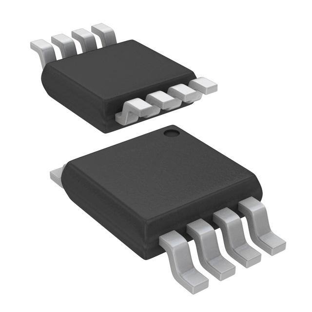
| 产品图片 |
|
| rohs | 符合RoHS无铅 / 符合限制有害物质指令(RoHS)规范要求 |
| 产品系列 | 电源管理 IC,电流和电力监控器、调节器,Texas Instruments INA201AIDGKT- |
| 数据手册 | |
| 产品型号 | INA201AIDGKT |
| 产品 | Current Monitors |
| 产品培训模块 | http://www.digikey.cn/PTM/IndividualPTM.page?site=cn&lang=zhs&ptm=12392 |
| 产品目录页面 | |
| 产品种类 | 电流和电力监控器、调节器 |
| 供应商器件封装 | 8-VSSOP |
| 其它名称 | 296-26069-2 |
| 准确性 | 3.5 % |
| 制造商产品页 | http://www.ti.com/general/docs/suppproductinfo.tsp?distId=10&orderablePartNumber=INA201AIDGKT |
| 功能 | 电流监控器 |
| 包装 | 带卷 (TR) |
| 单位重量 | 26.500 mg |
| 商标 | Texas Instruments |
| 安装类型 | 表面贴装 |
| 安装风格 | SMD/SMT |
| 封装 | Reel |
| 封装/外壳 | 8-TSSOP,8-MSOP(0.118",3.00mm 宽) |
| 封装/箱体 | VSSOP-8 |
| 工作温度 | -40°C ~ 125°C |
| 工作温度范围 | - 40 C to + 125 C |
| 工厂包装数量 | 250 |
| 感应方式 | High Side |
| 感应方法 | 高端 |
| 标准包装 | 250 |
| 电压-输入 | -16 V ~ 80 V |
| 电流-输出 | - |
| 电源电压-最大 | 18 V |
| 电源电压-最小 | 2.7 V |
| 电源电流 | 1.85 mA |
| 精度 | ±3.5% |
| 系列 | INA201 |
| 输入电压范围 | 2.7 V to 18 V |


- 商务部:美国ITC正式对集成电路等产品启动337调查
- 曝三星4nm工艺存在良率问题 高通将骁龙8 Gen1或转产台积电
- 太阳诱电将投资9.5亿元在常州建新厂生产MLCC 预计2023年完工
- 英特尔发布欧洲新工厂建设计划 深化IDM 2.0 战略
- 台积电先进制程称霸业界 有大客户加持明年业绩稳了
- 达到5530亿美元!SIA预计今年全球半导体销售额将创下新高
- 英特尔拟将自动驾驶子公司Mobileye上市 估值或超500亿美元
- 三星加码芯片和SET,合并消费电子和移动部门,撤换高东真等 CEO
- 三星电子宣布重大人事变动 还合并消费电子和移动部门
- 海关总署:前11个月进口集成电路产品价值2.52万亿元 增长14.8%


PDF Datasheet 数据手册内容提取
Product Order Technical Tools & Support & Reference Folder Now Documents Software Community Design INA200,INA201,INA202 SBOS374E–NOVEMBER2006–REVISEDSEPTEMBER2017 INA20x High-Side Measurement Current-Shunt Monitor With Open-Drain Comparator and Reference 1 Features 3 Description • CompleteCurrentSenseSolution The INA200, INA201, and INA202 devices are high- 1 side current-shunt monitors with voltage output and • ThreeGainOptionsAvailable: integrated comparator. The INA20x devices can – INA200=20V/V sense drops across shunts at common-mode – INA201=50V/V voltages from –16 V to 80 V. The INA20x series is available with three output voltage scales: 20 V/V, 50 – INA202=100V/V V/V,and100V/V,withabandwidthupto500-kHz. • 0.6-VInternalVoltageReference The INA200, INA201, and INA202 devices • InternalOpen-DrainComparator incorporate an open-drain comparator and internal • LatchingCapabilityonComparator reference providing a 0.6-V threshold. External • Common-ModeRange:–16Vto80V dividers set the current trip point. The comparator includes a latching capability, that can be made • HighAccuracy:3.5%MaximumErrorOver transparent by grounding (or leaving open) the Temperature RESETpin. • Bandwidth:500kHz(INA200) The INA200, INA201, and INA202 devices operate • QuiescentCurrent:1800μA(Maximum) from a single 2.7-V to 18-V supply, drawing a • Packages:SOIC-8,VSSOP-8 maximum of 1800 μA of supply current. Package optionsincludetheverysmallVSSOP-8andthe 2 Applications SOIC-8. All versions are specified over the extended operatingtemperaturerangeof –40°Cto+125°C. • NotebookComputers • CellPhones DeviceInformation(1) • TelecomEquipment PARTNUMBER PACKAGE BODYSIZE(NOM) • Automotive INA200 SOIC(8) 4.90mm×3.91mm • PowerManagement INA201 INA202 VSSOP(8) 3.00mm×3.00mm • BatteryChargers (1) For all available packages, see the orderable addendum at • WeldingEquipment theendofthedatasheet. SimplifiedSchematic INA200 (G = 20) INA201 (G = 50) 1 INA202 (G = 100) V S VIN+ 8 2 OUT G VIN- 7 0.6-V Reference 3 CMPIN Comparator CMPOUT 6 4 GND RESET 5 Copyright©2017,TexasInstrumentsIncorporated 1 An IMPORTANT NOTICE at the end of this data sheet addresses availability, warranty, changes, use in safety-critical applications, intellectualpropertymattersandotherimportantdisclaimers.PRODUCTIONDATA.
INA200,INA201,INA202 SBOS374E–NOVEMBER2006–REVISEDSEPTEMBER2017 www.ti.com Table of Contents 1 Features.................................................................. 1 7.3 FeatureDescription.................................................13 2 Applications........................................................... 1 7.4 DeviceFunctionalModes........................................19 3 Description............................................................. 1 8 ApplicationandImplementation........................ 22 4 RevisionHistory..................................................... 2 8.1 ApplicationInformation............................................22 8.2 TypicalApplication .................................................22 5 PinConfigurationandFunctions......................... 3 9 PowerSupplyRecommendations...................... 23 6 Specifications......................................................... 4 9.1 OutputvsSupplyRampConsiderations.................23 6.1 AbsoluteMaximumRatings......................................4 10 Layout................................................................... 25 6.2 ESDRatings..............................................................4 6.3 RecommendedOperatingConditions.......................4 10.1 LayoutGuidelines.................................................25 6.4 ThermalInformation..................................................4 10.2 LayoutExample....................................................25 6.5 ElectricalCharacteristics:Current-ShuntMonitor.....5 11 DeviceandDocumentationSupport................. 26 6.6 ElectricalCharacteristics:Comparator......................7 11.1 RelatedLinks........................................................26 6.7 ElectricalCharacteristics:General............................7 11.2 CommunityResources..........................................26 6.8 TypicalCharacteristics..............................................9 11.3 Trademarks...........................................................26 7 DetailedDescription............................................ 13 11.4 ElectrostaticDischargeCaution............................26 7.1 Overview.................................................................13 11.5 Glossary................................................................26 7.2 FunctionalBlockDiagram.......................................13 12 Mechanical,Packaging,andOrderable Information........................................................... 26 4 Revision History NOTE:Pagenumbersforpreviousrevisionsmaydifferfrompagenumbersinthecurrentversion. ChangesfromRevisionD(October2015)toRevisionE Page • ReformattedThermalInformationtablenote ......................................................................................................................... 4 • CorrectedtypoinVoltageOutputsectioninElectricalCharacteristicstable......................................................................... 6 • AddedtexttoComparatorsubsectioninFeatureDescriptionsection................................................................................. 14 • AddedFigure31toFeatureDescriptionsection.................................................................................................................. 18 • AddedOutputvsSupplyRampConsiderationssubsectioninFeatureDescriptionsection................................................ 23 • AddedFigure36,Figure37,andFigure38......................................................................................................................... 23 ChangesfromRevisionC(October2010)toRevisionD Page • AddedESDRatingstable,ThermalInformationtable,FeatureDescriptionsection,DeviceFunctionalModes, ApplicationandImplementationsection,PowerSupplyRecommendationssection,Layoutsection,Deviceand DocumentationSupportsection,andMechanical,Packaging,andOrderableInformationsection ..................................... 4 ChangesfromRevisionB(October,2007)toRevisionC Page • Revisedfront-pagefigure....................................................................................................................................................... 1 • Changedtitleofdatasheet..................................................................................................................................................... 1 • Updateddocumentformattocurrentstandards..................................................................................................................... 1 2 SubmitDocumentationFeedback Copyright©2006–2017,TexasInstrumentsIncorporated ProductFolderLinks:INA200 INA201 INA202
INA200,INA201,INA202 www.ti.com SBOS374E–NOVEMBER2006–REVISEDSEPTEMBER2017 5 Pin Configuration and Functions DGKandDPackages 8-PinVSSOPandSOIC TopView V 1 8 V S IN+ OUT 2 7 V IN- CMP 3 6 CMP IN OUT GND 4 5 RESET PinFunctions PIN I/O DESCRIPTION NAME NO. CMP 3 Analoginput Comparatorinput IN Analog CMP 6 Comparatoroutput OUT output GND 4 Analog Ground Analog OUT 2 Outputvoltage output RESET 5 Analoginput Comparatorresetpin,activelow V 7 Analoginput Connecttoshuntlowside IN– V 8 Analoginput Connecttoshunthighside IN+ V 1 Analog Powersupply S Copyright©2006–2017,TexasInstrumentsIncorporated SubmitDocumentationFeedback 3 ProductFolderLinks:INA200 INA201 INA202
INA200,INA201,INA202 SBOS374E–NOVEMBER2006–REVISEDSEPTEMBER2017 www.ti.com 6 Specifications 6.1 Absolute Maximum Ratings overoperatingfree-airtemperaturerange(unlessotherwisenoted)(1) MIN MAX UNIT Supplyvoltage,V 2.7 18 V s Current-shuntmonitor Differential(VIN+)–(VIN–) –18 18 V analoginputs,VIN+,VIN– Common-mode(2) –16 80 V Comparatoranaloginputandresetpins(2) GND–0.3 (V )+0.3 V s Analogoutput,OUT(2) GND–0.3 (V )+0.3 V s Comparatoroutput,OUT(2) GND–0.3 18 V Inputcurrentintoanypin(2) 5 mA Operatingtemperature –55 150 °C Junctiontemperature –65 150 °C Storagetemperature,T –65 150 °C stg (1) StressesbeyondthoselistedunderAbsoluteMaximumRatingsmaycausepermanentdamagetothedevice.Thesearestressratings only,whichdonotimplyfunctionaloperationofthedeviceattheseoranyotherconditionsbeyondthoseindicatedunderRecommended OperatingConditions.Exposuretoabsolute-maximum-ratedconditionsforextendedperiodsmayaffectdevicereliability. (2) Thisvoltagemayexceedtheratingsshownifthecurrentatthatpinislimitedto5mA. 6.2 ESD Ratings VALUE UNIT Humanbodymodel(HBM),perANSI/ESDA/JEDECJS-001,allpins(1) ±4000 V(ESD) Electrostaticdischarge Chargeddevicemodel(CDM),perJEDECspecificationJESD22-C101,all V pins(2) ±1000 (1) JEDECdocumentJEP155statesthat500-VHBMallowssafemanufacturingwithastandardESDcontrolprocess. (2) JEDECdocumentJEP157statesthat250-VCDMallowssafemanufacturingwithastandardESDcontrolprocess. 6.3 Recommended Operating Conditions overoperatingfree-airtemperaturerange(unlessotherwisenoted) MIN NOM MAX UNIT V Common-modeinputvoltage –16 12 80 V CM V Operatingsupplyvoltage 2.7 12 18 V S T Operatingfree-airtemperature –40 25 125 °C A 6.4 Thermal Information INA20x THERMALMETRIC(1) D(SOIC) DGK(SOIC) UNIT 8PINS 8PINS R Junction-to-ambientthermalresistance 110.5 162.2 °C/W θJA R Junction-to-case(top)thermalresistance 50.4 37.7 °C/W θJC(top) R Junction-to-boardthermalresistance 52.7 82.9 °C/W θJB ψ Junction-to-topcharacterizationparameter 7.8 1.3 °C/W JT ψ Junction-to-boardcharacterizationparameter 51.9 81.4 °C/W JB (1) Formoreinformationabouttraditionalandnewthermalmetrics,seetheSemiconductorandICPackageThermalMetricsapplication report. 4 SubmitDocumentationFeedback Copyright©2006–2017,TexasInstrumentsIncorporated ProductFolderLinks:INA200 INA201 INA202
INA200,INA201,INA202 www.ti.com SBOS374E–NOVEMBER2006–REVISEDSEPTEMBER2017 6.5 Electrical Characteristics: Current-Shunt Monitor atT =25°C,V =12V,V =12V,V =100mV,R =10kΩtoGND,R =5.1kΩconnectedfromCMP toV , A S CM SENSE L PULL-UP OUT S andCMP =GND,(unlessotherwisenoted) IN PARAMETER TESTCONDITIONS MIN TYP MAX UNIT INPUT VSENSE Full-scalesenseinputvoltage VSENSE=VIN+ –VIN– 0.15 (VS –0.25)/Gain V VCM Common-modeinputrange TA=–40°Cto125°C –16 80 V VIN+=–16Vto80V 80 100 dB CMR Common-moderejection VIN+=12Vto80V,TA=–40°Cto125°C 100 123 dB TA=25°C ±0.5 ±2.5 mV VOS Offsetvoltage,RTI(1) TA=25°Cto125°C ±3 mV TA=–40°Cto25°C ±3.5 mV Offsetvoltage,RTI,vs dVOS/dT temperature TMINtoTMAX,TA=–40°Cto125°C 5 μV/°C PSR Offsetvoltage,RTI,vspower VOUT=2V,VIN+=18V,2.7V,TA=–40°Cto 2.5 100 μV/V supply 125°C IB Inputbiascurrent,VIN–pin TA=–40°Cto125°C ±9 ±16 μA (1) Offsetisextrapolatedfrommeasurementsoftheoutputat20-mVand100-mVV . SENSE Copyright©2006–2017,TexasInstrumentsIncorporated SubmitDocumentationFeedback 5 ProductFolderLinks:INA200 INA201 INA202
INA200,INA201,INA202 SBOS374E–NOVEMBER2006–REVISEDSEPTEMBER2017 www.ti.com Electrical Characteristics: Current-Shunt Monitor (continued) atT =25°C,V =12V,V =12V,V =100mV,R =10kΩtoGND,R =5.1kΩconnectedfromCMP toV , A S CM SENSE L PULL-UP OUT S andCMP =GND,(unlessotherwisenoted) IN PARAMETER TESTCONDITIONS MIN TYP MAX UNIT OUTPUT(VSENSE ≥20mV) INA200 20 V/V G Gain INA201 50 V/V INA202 100 V/V VSENSE=20mVto100mV ±0.2% ±1% Gainerror VSENSE=20mVto100mV,TA=–40°Cto ±2% 125°C VSENSE=120mV,VS=16V ±0.75% ±2.2% Totaloutputerror(2) VSENSE=120mV,VS=16V,TA=–40°Cto ±3.5% 125°C Nonlinearityerror(3) VSENSE=20mVto100mV ±0.002% RO Outputimpedance 1.5 Ω Maximumcapacitiveload Nosustainedoscillation 10 nF OUTPUT(VSENSE<20mV)(4) INA200,INA201, INA202 –16V≤VCM<0V 300 mV INA200 0V≤VCM≤VS,VS= 0.4 V 5V Output INA201 0V≤VCM≤VS,VS= 1 V 5V INA202 0V≤VCM≤VS,VS= 2 V 5V INA200,INA201, INA202 VS<VCM≤80V 300 mV VOLTAGEOUTPUT(5) Outputswingtothepositiverail VIN–=11V,VIN+=12V,TA=–40°Cto125°C (Vs)–0.15 (Vs)–0.25 V OutputswingtoGND(6) VIN–=0V,VIN+=–0.5V,TA=–40°Cto125°C (GND)+0.004 (GND)+0.05 V FREQUENCYRESPONSE INA200 CLOAD=5pF 500 kHz BW Bandwidth INA201 CLOAD=5pF 300 kHz INA202 CLOAD=5pF 200 kHz Phasemargin CLOAD<10nF 40 °C SR Slewrate 1 V/μs Settlingtime(1%) VSENSE=10mVPPto100mVPP, 2 μs CLOAD=5pF NOISE,RTI Voltagenoisedensity 40 nV/√Hz (2) TotaloutputerrorincludeseffectsofgainerrorandV . OS (3) Linearityisbestfittoastraightline. (4) Fordetailsonthisregionofoperation,seeAccuracyVariationssectioninDeviceFunctionalModes. (5) SeeFigure8. (6) Specifiedbydesign. 6 SubmitDocumentationFeedback Copyright©2006–2017,TexasInstrumentsIncorporated ProductFolderLinks:INA200 INA201 INA202
INA200,INA201,INA202 www.ti.com SBOS374E–NOVEMBER2006–REVISEDSEPTEMBER2017 6.6 Electrical Characteristics: Comparator atT =25°C,V =12V,V =12V,V =100mV,R =10kΩtoGND,andR =5.1kΩconnectedfromCMP to A S CM SENSE L PULL-UP OUT V ,(unlessotherwisenoted) S PARAMETER TESTCONDITIONS MIN TYP MAX UNIT OFFSETVOLTAGE TA=25°C 590 608 620 mV Threshold TA=–40°Cto125°C 586 625 mV Hysteresis(1) TA=–40°Cto85°C –8 mV INPUTBIASCURRENT(2) Inputbiascurrent,CMPinPIN 0.005 10 nA Inputbiascurrent,CMPinPIN,vstemperature TA=–40°Cto125°C 15 nA INPUTVOLTAGERANGE Inputvoltagerange,CMPinPIN 0VtoVS–1.5V V OUTPUT(OPEN-DRAIN) Large-signaldifferentialvoltagegain CMPVOUT1Vto4V, 200 V/mV RL≥15kΩconnectedto5V ILKG High-levelleakagecurrent(3)(4) VID=0.4V,VOH=VS 0.0001 1 μA VOL Low-leveloutputvoltage(3) VID=–0.6V,IOL=2.35mA 220 300 mV RESPONSETIME Responsetime(5) RLto5V,CL=15pF,100-mVInput 1.3 μs Stepwith5-mVoverdrive RESET RESETthreshold(6) 1.1 V Logicinputimpedance 2 MΩ MinimumRESETpulsewidth 1.5 μs RESETpropagationdelay 3 μs (1) Hysteresisreferstothethreshold(thethresholdspecificationappliestoarisingedgeofanoninvertinginput)ofafallingedgeonthe noninvertinginputofthecomparator;refertoFigure1. (2) Specifiedbydesign. (3) V referstothedifferentialvoltageatthecomparatorinputs. ID (4) Open-drainoutputcanbepulledtotherangeof2.7to18V,regardlessofV . S (5) Thecomparatorresponsetimespecifiedistheintervalbetweentheinputstepfunctionandtheinstantwhentheoutputcrosses1.4V. (6) TheRESETinputhasaninternal2MΩ(typical)pull-down.LeavingRESETopenresultsinaLOWstate,withtransparentcomparator operation. 6.7 Electrical Characteristics: General atT =25°C,V =12V,V =12V,V =100mV,R =10kΩtoGND,R =5.1kΩconnectedfromCMP toV , A S CM SENSE L PULL-UP OUT S andCMP =1V,unlessotherwisenoted. IN PARAMETER TESTCONDITIONS MIN TYP MAX UNIT POWERSUPPLY VS Operatingpowersupply TA=–40°Cto125°C 2.7 18 V VOUT=2V 1350 1800 μA IQ Quiescentcurrent VSENSE=0mV,TA=–40°Cto125°C 1850 μA Comparatorpower-onreset threshold(1) 1.5 V TEMPERATURE Specifiedtemperature –40 125 °C Operatingtemperature –55 150 °C Storagetemperature –65 150 °C VSSOP-8Surface-Mount 200 °C/W θJA Thermalresistance SOIC-8 150 °C/W (1) TheINA200,INA201,andINA202aredesignedtopower-upwiththecomparatorinadefinedresetstateaslongasRESETisopenor grounded.Thecomparatorisinresetaslongasthepowersupplyisbelowthevoltageshownhere.Thecomparatorassumesastate basedonthecomparatorinputabovethissupplyvoltage.IfRESETishighatpower-up,thecomparatoroutputcomesuphighand requiresaresettoassumealowstate,ifappropriate. Copyright©2006–2017,TexasInstrumentsIncorporated SubmitDocumentationFeedback 7 ProductFolderLinks:INA200 INA201 INA202
INA200,INA201,INA202 SBOS374E–NOVEMBER2006–REVISEDSEPTEMBER2017 www.ti.com V THRESHOLD 0.592V 0.6V Input Voltage Hysteresis = V -8mV THRESHOLD Figure1. TypicalComparatorHysteresis 8 SubmitDocumentationFeedback Copyright©2006–2017,TexasInstrumentsIncorporated ProductFolderLinks:INA200 INA201 INA202
INA200,INA201,INA202 www.ti.com SBOS374E–NOVEMBER2006–REVISEDSEPTEMBER2017 6.8 Typical Characteristics atT =25°C,V =12V,V =12V,andV =100mV,(unlessotherwisenoted) A S IN+ SENSE 45 45 G = 100 CLOAD= 1000pF G = 100 40 40 35 G = 50 35 G = 50 dB) 30 G = 20 dB) 30 G = 20 n ( 25 n ( 25 ai ai G G 20 20 15 15 10 10 5 5 10k 100k 1M 10k 100k 1M Frequency (Hz) Frequency (Hz) Figure2.GainvsFrequency Figure3.GainvsFrequency 20 140 18 130 16 100V/V B) 120 V(V)OUT 1114208 50V/V mon-Mode andpply Rejection (d 1110980000 CMRPSR 20V/V mSu 6 Coer- 70 w 4 o 60 P 2 50 0 40 20 100 200 300 400 500 600 700 800 900 10 100 1k 10k 100k V (mV) Frequency (Hz) DIFFERENTIAL Figure4.GainPlot Figure5.Common-ModeandPower-SupplyRejectionvs Frequency 4.0 0.1 e) 3.5 0.09 u Output Erroror of the ideal output val 32211.....05050 Output Error (% ) 000000......000000876543 err 0.02 % 0.5 ( 0.01 0 0 0 50 100 150 200 250 300 350 400 450 500 -16-12 -8 -4 0 4 8 12 16 20 ... 76 80 VSENSE(mV) Common-Mode Voltage (V) Figure6.OutputErrorvsVSENSE Figure7.OutputErrorvsCommon-ModeVoltage Copyright©2006–2017,TexasInstrumentsIncorporated SubmitDocumentationFeedback 9 ProductFolderLinks:INA200 INA201 INA202
INA200,INA201,INA202 SBOS374E–NOVEMBER2006–REVISEDSEPTEMBER2017 www.ti.com Typical Characteristics (continued) atT =25°C,V =12V,V =12V,andV =100mV,(unlessotherwisenoted) A S IN+ SENSE 12 3.5 11 10 VS= 12V 3.0 Sourcing Current 9 V) +25°C 2.5 Voltage ( 876 V = 3V +125°C -40°C (mA) 2.0 put 5 SSourcing Current IQ 1.5 Out 4 +25°C -40°C Output stage is designed 1.0 3 to source current. Current 2 sinking capability is 0.5 1 approximately 400mA. +125°C 0 0 0 5 10 15 20 25 30 0 1 2 3 4 5 6 7 8 9 10 Output Current (mA) Output Voltage (V) Figure8.PositiveOutputVoltageSwingvsOutputCurrent Figure9.QuiescentCurrentvsOutputVoltage 2.00 VSENSE= 100mV 34 -40°C 11..7550 VS= 12V VS= 2.7V urrent (mA) 3206 +125°+C25°C C I(mA)Q11..2050 VS= 12V ort-Circuit 2128 VSENSE= 0mV VS= 2.7V ut Sh 14 0.75 utp 10 O 0.50 6 -16 -12 -8 -4 0 4 8 12 16 20 24 28 32 36 2.5 3.5 4.5 5.5 6.5 7.5 8.5 9.5 10.5 11.5 17 18 VCM(V) Supply Voltage (V) Figure10.QuiescentCurrentvsCommon-ModeVoltage Figure11.OutputShort-CircuitCurrentvsSupplyVoltage G = 20 G = 20 mV/div) mV/div) Output Voltage (50 Output Voltage (500 V = 20mV to 30mV V = 20mV to 110mV SENSE SENSE Time (2ms/div) Time (2ms/div) Figure12.StepResponse Figure13.StepResponse 10 SubmitDocumentationFeedback Copyright©2006–2017,TexasInstrumentsIncorporated ProductFolderLinks:INA200 INA201 INA202
INA200,INA201,INA202 www.ti.com SBOS374E–NOVEMBER2006–REVISEDSEPTEMBER2017 Typical Characteristics (continued) atT =25°C,V =12V,V =12V,andV =100mV,(unlessotherwisenoted) A S IN+ SENSE G = 20 G = 50 mV/div) mV/div) Output Voltage (50 Output Voltage (100 VSENSE= 90mV to 100mV VSENSE= 20mV to 30mV Time (2ms/div) Time (5ms/div) Figure14.StepResponse Figure15.StepResponse G = 50 G = 50 div) V/div) V/ m Output Voltage (1 utput Voltage (100 O VSENSE= 20mV to 110mV VSENSE= 90mV to 100mV Time (5ms/div) Time (5ms/div) Figure16.StepResponse Figure17.StepResponse 600 G = 100 500 v) V/di 400 ge (2 (mV) 300 olta VOL ut V 200 p Out 100 V = 20mV to 110mV 0 SENSE 0 1 2 3 4 5 6 Time (10ms/div) ISINK(mA) Figure18.StepResponse Figure19.ComparatorVOLvsISINK Copyright©2006–2017,TexasInstrumentsIncorporated SubmitDocumentationFeedback 11 ProductFolderLinks:INA200 INA201 INA202
INA200,INA201,INA202 SBOS374E–NOVEMBER2006–REVISEDSEPTEMBER2017 www.ti.com Typical Characteristics (continued) atT =25°C,V =12V,V =12V,andV =100mV,(unlessotherwisenoted) A S IN+ SENSE 600 602 599 598 V) 601 m mV) 597 nt ( 600 et Voltage ( 555999654 ator Trip Poi 599 Res 593 mpar 598 592 Co 597 591 590 596 2 4 6 8 10 12 14 16 18 -50 -25 0 25 50 75 100 125 Supply Voltage (V) Temperature (°C) Figure20.ComparatorTripPointvsSupplyVoltage Figure21.ComparatorTripPointvsTemperature 200 1.2 175 1.0 Delay (ns) 150 age (V) 0.8 opagation 112050 Reset Volt 00..64 Pr 75 0.2 50 0 0 20 40 60 80 100 120 140 160 180 200 2 4 6 8 10 12 14 16 18 Overdrive Voltage (mV) Supply Voltage (V) Figure22.ComparatorPropagationDelayvsOverdrive Figure23.ComparatorResetVoltagevsSupplyVoltage Voltage 300 275 s) Input n 250 y ( 200mV/div a Del 225 n o ati 200 g a op 175 Pr Output 150 2V/div 125 V = 5mV -50 -25 0 25 50 75 100 125 OD Temperature (°C) 2ms/div Figure24.ComparatorPropagationDelayvsTemperature Figure25.ComparatorPropagationDelay 12 SubmitDocumentationFeedback Copyright©2006–2017,TexasInstrumentsIncorporated ProductFolderLinks:INA200 INA201 INA202
INA200,INA201,INA202 www.ti.com SBOS374E–NOVEMBER2006–REVISEDSEPTEMBER2017 7 Detailed Description 7.1 Overview The INA200, INA201, and INA202 devices are high-side current-shunt monitors with voltage output. The INA20x devices can sense drops across shunts at common-mode voltages from –16 V to 80 V. The INA200–INA202 devices are available with three output voltage scales: 20 V/V, 50 V/V, and 100 V/V, with up to 500-kHz bandwidth. The INA200, INA201, and INA202 devices incorporate an open-drain comparator and internal reference providing a 0.6-V threshold. External dividers set the current trip point. The comparator includes a latching capability, that can be made transparent by grounding (or leaving open) the RESET pin. The INA200, INA201, and INA202 devices operate from a single 2.7 to 18-V supply, drawing a maximum of 1800 μA of supply current. Package options include the very small MSOP-8 and the SO-8. All versions are specified over the extendedoperatingtemperaturerangeof–40°Cto+125°C. 7.2 Functional Block Diagram VS VIN+ OUT G VIN- 0.6-V Reference CMPIN Comparator CMPOUT RESET GND 7.3 Feature Description 7.3.1 BasicConnections Figure 26 shows the basic connections of the INA20x devices. The input pins (V and V ) must be connected IN+ IN– as closely as possible with Kelvin connections to the shunt resistor to minimize any resistance in series with the shuntresistance. Power-supply bypass capacitors are required for stability. Applications with noisy or high-impedance power supplies may require additional decoupling capacitors to reject power-supply noise. Connect bypass capacitors closetothedevicepins. Copyright©2006–2017,TexasInstrumentsIncorporated SubmitDocumentationFeedback 13 ProductFolderLinks:INA200 INA201 INA202
INA200,INA201,INA202 SBOS374E–NOVEMBER2006–REVISEDSEPTEMBER2017 www.ti.com RSHUNT 3 m(cid:13) Load Supply Load -18 V to 80 V 5-V Supply INA200 1 (G = 20) VS VIN+ 8 RPULLUP 2 OUT 4.7 k(cid:13) G VIN- 7 CBYPASS 0.01 µF R1 Re0fe.6re-Vnce 3 CMPIN CMPOUT 6 Comparator R2 4 GND RESET 5 SW Transparent / Reset Latch Copyright © 2017, Texas Instruments Incorporated Figure26. INA200BasicConnections 7.3.2 SelectingR S The selected value for the shunt resistor, R , depends on the application and is a compromise between small- S signalaccuracyandmaximumpermissiblevoltagelossinthemeasurementline.HighvaluesofR providebetter S accuracy at lower currents by minimizing the effects of offset, while low values of R minimize voltage loss in the S supply line. For most applications, using an R value that provides a full-scale shunt voltage range of 50 mV to S 100 mV results in the best performance. Maximum input voltage for accurate measurements is 500 mV, but outputvoltageislimitedbysupply. 7.3.3 Comparator The INA200, INA201, and INA202 devices incorporate an open-drain comparator. This comparator typically has 2 mV of offset and a 1.3-μs (typical) response time. The output of the comparator latches and is reset through the RESETpin;seeFigure28. When V and RESET are different, TI recommends adding a low-pass filter (LPF) on the RESET pin to avoid s comparator behavior inconsistent with the data sheet. For instance, with a 12-V supply and a 3.3-V RESET, a rise time of 400 ns is appropriate. Similarly, with an 18-V supply and a 2.7-V RESET, a 1-µs rise time is appropriate;seeFigure31. 14 SubmitDocumentationFeedback Copyright©2006–2017,TexasInstrumentsIncorporated ProductFolderLinks:INA200 INA201 INA202
INA200,INA201,INA202 www.ti.com SBOS374E–NOVEMBER2006–REVISEDSEPTEMBER2017 RSHUNT << RFILTER 3 m(cid:13) VSUPPLY Load INA200-INA202 RFILTER < 100 (cid:13) RFILTER < 100 (cid:13) CFILTER VS VIN+ OUT G VIN- 0.6-V Reference f-3dB CMPIN Comparator CMPOUT f-3dB = 2(cid:140)(2RFILT1ER)CFILTER RESET GND SO-14, TSSOP-14 Copyright © 2017, Texas Instruments Incorporated Figure27. InputFilter(GainError:1.5%to2.8%) 0.6V V IN 0V CMP OUT RESET Figure28. ComparatorLatchingCapability Copyright©2006–2017,TexasInstrumentsIncorporated SubmitDocumentationFeedback 15 ProductFolderLinks:INA200 INA201 INA202
INA200,INA201,INA202 SBOS374E–NOVEMBER2006–REVISEDSEPTEMBER2017 www.ti.com Shunt Shunt Option 1 Option 2 Supply R 3 To V To V To V To V IN+ IN- IN+ IN- 4.5 V to 5.5 V R 4 Q 1 2N3904 Load INA200 (G = 20) 1 INA201 (G = 50) V INA202 (G = 100) S To V IN+ VIN+ 8 Shunt 2 OUT From Option 3 G Shunt Option VIN- 7 1, 2, or 3 To VIN- 0.6-V R 1 Reference 3 CMPIN CMP 6 R Comparator OUT 2 4 RESET 5 GND RESET Copyright © 2017,Texas Instruments Incorporated (1) Q1cascodesthecomparatoroutputtodriveahigh-sideFET(the2N3904)shownisgoodupto60V.Theshuntcan belocatedinanyoneofthethreelocationsshown.Thelatchingcapabilitymustbeusedinshutdownapplicationsto preventoscillationatthetrippoint. Figure29. High-SideSwitchOvercurrentShutdown 16 SubmitDocumentationFeedback Copyright©2006–2017,TexasInstrumentsIncorporated ProductFolderLinks:INA200 INA201 INA202
INA200,INA201,INA202 www.ti.com SBOS374E–NOVEMBER2006–REVISEDSEPTEMBER2017 RSHUNT Supply 4.5 V to 5.5 V INA200 (G = 20) INA201 (G = 50) 1 VS INA202 (G = 100) VIN+ 8 R5 2.2 k(cid:13) 2 OUT G VIN- 7 0.6-V R3 Reference 3 CMPIN CMPOUT 6 Comparator R4 4 RESET 5 GND INA200 (G = 20) 1 INA201 (G = 50) VS INA202 (G = 100) R6 2.2 k(cid:13) VIN+ 8 2 OUT G VIN- 7 0.6-V R3 Reference 3 CMPIN Comparator CMPOUT 6 CMPOUT R4 4 RESET 5 R7 200 k(cid:13) GND Copyright © 2017, Texas Instruments Incorporated (1) Itispossibletosetdifferentlimitsforeachdirection. Figure30. BidirectionalOvercurrentComparator Copyright©2006–2017,TexasInstrumentsIncorporated SubmitDocumentationFeedback 17 ProductFolderLinks:INA200 INA201 INA202
INA200,INA201,INA202 SBOS374E–NOVEMBER2006–REVISEDSEPTEMBER2017 www.ti.com VS VIN+ OUT G VIN- 0.6-V Reference CMPIN Comparator CMPOUT Rf RESET 5 GND Controller Cf GND Figure31. FilteronRESETPin 18 SubmitDocumentationFeedback Copyright©2006–2017,TexasInstrumentsIncorporated ProductFolderLinks:INA200 INA201 INA202
INA200,INA201,INA202 www.ti.com SBOS374E–NOVEMBER2006–REVISEDSEPTEMBER2017 7.4 Device Functional Modes 7.4.1 InputFiltering An obvious and straightforward location for filtering is at the output of the INA20x series; however, this location negates the advantage of the low output impedance of the internal buffer. The only other option for filtering is at the input pins of the INA20x devices, which is complicated by the internal 5 kΩ + 30% input impedance. This is shown in Figure 27. Using the lowest possible resistor values minimizes the initial shift in gain and effects of tolerance.TheeffectoninitialgainisshowninEquation1: 5kW Gain Error % = 100- 100´ 5kW+ R FILT (1) Total effect on gain error can be calculated by replacing the 5-kΩ term with 5 kΩ – 30%, (or 3.5 kΩ) or 5 kΩ + 30% (or 6.5 kΩ). The tolerance extremes of R can be inserted into the equation. If a pair of 100-Ω 1% FILT resistors are used on the inputs, the initial gain error equals 1.96%. Worst-case tolerance conditions always occur at the lower excursion of the internal 5-kΩ resistor (3.5 kΩ), and the higher excursion of R – 3% in this FILT case. The specified accuracy of the INA20x devices must then be combined in addition to these tolerances. While this discussion treated accuracy worst-case conditions by combining the extremes of the resistor values, it is appropriatetousegeometricmeanorrootsumsquarecalculationstototaltheeffectsofaccuracyvariations. 7.4.2 AccuracyVariationsasaResultofV andCommon-ModeVoltage SENSE The accuracy of the INA200, INA201, and INA202 current shunt monitors is a function of two main variables: V (V – V ), common-mode voltage, (V ), relative to the supply voltage (V ). V is expressed as (V SENSE IN+ IN– CM S CM IN+ + V ) / 2; however, in practice, V is seen as the voltage at V because the voltage drop across V is IN– CM IN+ SENSE typicallysmall. Thissectionaddressestheaccuracyofthesespecificoperatingregions: • NormalCase1:V ≥20mV,V ≥ V SENSE CM S • NormalCase2:V ≥20mV,V < V SENSE CM S • LowV Case1:V <20mV, –16V≤ V < 0 SENSE SENSE CM • LowV Case2:V <20mV,0V≤ V ≤ V SENSE SENSE CM S • LowV Case3:V <20mV,V <V ≤ 80V SENSE SENSE S CM 7.4.2.1 NormalCase1:V ≥20mv,V ≥ V SENSE CM S This region of operation provides the highest accuracy. Here, the input offset voltage is characterized and measuredusingatwo-stepmethod.First,thegainisdeterminedbyEquation2. V -V G = OUT1 OUT2 100mV-20mV where • V =outputvoltagewithV =100mV OUT1 SENSE • V =outputvoltagewithV =20mV (2) OUT2 SENSE Then the offset voltage is measured at V = 100 mV, and referred to the input (RTI) of the current shunt SENSE monitor,asshowninElectricalCharacteristics:Current-ShuntMonitor. V V RTI (Referred-To-Input) = OUT1 -100mV OS G (3) In the Typical Characteristics, Figure 7 shows the highest accuracy for the this region of operation. In this plot, V = 12 V. For V ≥ 12 V, the output error is at the minimum value. This case creates the V ≥ 20-mV S CM SENSE outputspecificationsinElectricalCharacteristics:Current-ShuntMonitor . Copyright©2006–2017,TexasInstrumentsIncorporated SubmitDocumentationFeedback 19 ProductFolderLinks:INA200 INA201 INA202
INA200,INA201,INA202 SBOS374E–NOVEMBER2006–REVISEDSEPTEMBER2017 www.ti.com Device Functional Modes (continued) 7.4.2.2 NormalCase2:V ≥20mv,V < V SENSE CM S This region of operation is less accurate than normal case 1 as a result of the common-mode operating area in which the part functions, as shown in the Figure 7 curve (Figure 7). As noted, for this graph V = 12 V; for V < S CM 12 V, the output error increases as V decreases to less than 12 V, with a typical maximum error of 0.005% at CM themostnegativeV =–16V. CM 7.4.2.3 LowV Case1:V <20mV, –16V ≤ V <0 SENSE SENSE CM andLowV Case3:V <20mV,V <V ≤ 80V SENSE SENSE S CM Although the INA200 family of devices are not designed for accurate operation in these regions, some applications are exposed to these conditions. For example, when monitoring power supplies that are switched on and off while V is still applied to the INA20x devices, it is important to know what the behavior of the devices is S intheseregions. As V approaches 0 mV, in these V regions, the accuracy of the device output degrades. A larger-than- SENSE CM normal offset can appear at the current shunt monitor output with a typical maximum value of V = 300 mV for OUT V = 0 mV. As V approaches 20 mV, V returns to the expected output value with accuracy as SENSE SENSE OUT shown in Electrical Characteristics: Current-Shunt Monitor. Figure 32 shows this effect using the INA202 (gain = 100). 2.0 1.8 1.6 1.4 V) 1.2 Actual ( T 1.0 U O V 0.8 Ideal 0.6 0.4 0.2 0 0 2 4 6 8 10 12 14 16 18 20 V (mV) SENSE Figure32. ExampleForLowV Cases1and3(INA202,Gain=100) SENSE 7.4.2.4 LowV Case2:V <20mV,0V ≤ V ≤ V SENSE SENSE CM S This region of operation is the least accurate for the INA20x family. To achieve the wide input common-mode voltage range, these devices use two op amp front ends in parallel. One op amp front end operates in the positive input common-mode voltage range, and the other in the negative input region. For this case, neither of thesetwointernalamplifiersdominatesandoverallloopgainislow.Withinthisregion,V approachesvoltages OUT close to linear operation levels for normal case 2. This deviation from linear operation becomes greatest the closerV approaches0V.Withinthisregion,asV approaches20mV,deviceoperationisclosertothat SENSE SENSE is described in normal case 2. Figure 33 shows this behavior for the INA202. The V maximum peak for this OUT caseistestedbymaintainingaconstantV ,settingV equalto0mVandsweepingV from0VtoV .The S SENSE CM S exact V at which V peaks during this test varies from device to device, but the V maximum peak is CM OUT OUT testedtobelessthanthespecifiedV testedlimit. OUT 20 SubmitDocumentationFeedback Copyright©2006–2017,TexasInstrumentsIncorporated ProductFolderLinks:INA200 INA201 INA202
INA200,INA201,INA202 www.ti.com SBOS374E–NOVEMBER2006–REVISEDSEPTEMBER2017 Device Functional Modes (continued) 2.4 (1) 2.2 INA202 VOUTTested Limit V 2.0 CM1 Ideal 1.8 V CM2 1.6 V) 1.4 ( V T 1.2 CM3 U O V 1.0 V tested limit at 0.8 VCM4 VOSEUNTSE= 0mV, 0£VCM1£VS. 0.6 V , V , and V illustrate the variance 0.4 CM2 CM3 CM4 from part to part of the V that can cause CM 0.2 maximum V with V < 20mV. OUT SENSE 0 0 2 4 6 8 10 12 14 16 18 20 22 24 V (mV) SENSE NOTE: (1) INA200 V Tested Limit = 0.4V. INA201 V Tested Limit = 1V. OUT OUT Figure33. ExampleForLowV Case2(INA202,Gain=100) SENSE 7.4.3 TransientProtection The –16 to 80 V common-mode range of the INA20x devices is ideal for withstanding automotive fault conditions ranging from 12-V battery reversal up to 80-V transients, since no additional protective components are required up to those levels. In the event that the INA20x devices are exposed to transients on the inputs in excess of their ratings, then external transient absorption with semiconductor transient absorbers (such as Zeners) are required. TI does not recommend using MOVs or VDRs, except when they are used in addition to a semiconductor transient absorber. Select the transient absorber so the absorber does not allow the INA20x devices to be exposed to transients greater than 80 V (that is, allow for transient absorber tolerance and additional voltage due to transient absorber dynamic impedance). Despite the use of internal Zener-type ESD protection, the INA20x devices do not lend themselves to using external resistors in series with the inputs since the internal gain resistors can vary up to ±30%. (If gain accuracy is not important, then resistors can be added in series with the INA200,INA201,andINA202inputswithtwoequalresistorsoneachinput.) 7.4.4 OutputVoltageRange The output of the INA20x devices is accurate within the output voltage swing range set by the power supply pin (V .) This performance is best illustrated when using the INA202 (a gain of 100 version), where a 100-mV full- S scale input from the shunt resistor requires an output voltage swing of 10 V, and a power-supply voltage sufficienttoachieve10Vontheoutput. Copyright©2006–2017,TexasInstrumentsIncorporated SubmitDocumentationFeedback 21 ProductFolderLinks:INA200 INA201 INA202
INA200,INA201,INA202 SBOS374E–NOVEMBER2006–REVISEDSEPTEMBER2017 www.ti.com 8 Application and Implementation NOTE Information in the following applications sections is not part of the TI component specification, and TI does not warrant its accuracy or completeness. TI’s customers are responsible for determining suitability of components for their purposes. Customers should validateandtesttheirdesignimplementationtoconfirmsystemfunctionality. 8.1 Application Information The INA20x series is designed to enable simple configuration for detecting overcurrent conditions and current monitoring in an application. This device is individually targeted towards overcurrent detection of a single threshold. However, this device can pair with additional devices and circuitry to create more complex monitoring functionalblocks. 8.2 Typical Application RSHUNT Supply To VIN+ To VIN- 4.5 V to 5.5 V Load To VIN+ Shunt INA200 (G = 20) Option 2 1 INA201 (G = 50) R4 2.2 k(cid:13) VS INA202 (G = 100) To VIN- VIN+ 8 2 OUT G FSrhoumnt Option R1 22 k(cid:13) VIN- 7 1, 2, or 3 R3 Re0fe.6re-Vnce To VIN+ Shunt Option 3 3 CMPIN CMPOUT 6 To VIN- Comparator Q1 2N3904 R4 4 RESET 5 GND Copyright © 2017, Texas Instruments Incorporated (1) Inthiscase,Qinvertsthecomparatoroutput. Figure34. Low-SideSwitchOvercurrentShutdown 8.2.1 DesignRequirements The device measures current through a resistive shunt with current flowing in one direction that enables detection of an overcurrent event only when the differential input voltage exceeds the threshold limit. When the current reaches the set limit of the divider R / R , the output of CMP transitions high, which turns Q1 on, 1 2 OUT pullsthegateofthepass-FETlow,andturnsofftheflowoffcurrent. 22 SubmitDocumentationFeedback Copyright©2006–2017,TexasInstrumentsIncorporated ProductFolderLinks:INA200 INA201 INA202
INA200,INA201,INA202 www.ti.com SBOS374E–NOVEMBER2006–REVISEDSEPTEMBER2017 Typical Application (continued) 8.2.2 DetailedDesignProcedure Figure 34 shows the basic connections of the device. The input terminals (IN+ and IN –) must be connected as closely as possible to the current-sensing resistor to minimize any resistance in series with the shunt resistance. Additional resistance between the current-sensing resistor and input terminals results in errors in the measurement. When input current flows through this external input resistance, the voltage developed across the shuntresistordiffersfromthevoltagereachingtheinputterminals. Use the gain of the INA20x and shunt value to calculate the OUT voltage for the desired trip current. Configure R1andR2sothatthecurrenttrippointisequaltothe0.6-Vreferencevoltage. 8.2.3 ApplicationCurve 1.2 Comp_IN I_Load CMP_OUT OUT 1 0.8 0.6 0.4 0.2 0 0 0.1 0.2 0.3 0.4 0.5 0.6 0.7 0.8 0.9 1 *Time Figure35.Low-SideSwitchOvercurrentShutdownResponse 9 Power Supply Recommendations The input circuitry of the INA20x devices can accurately measure beyond the power-supply voltage, V . For s example, the V power supply is 5 V, whereas the load power-supply voltage is up to 80 V. However, the output s voltagerangeoftheOUTpinislimitedbythevoltagesonthepowersupplypin. 9.1 Output vs Supply Ramp Considerations Figure36,Figure37,andFigure38showthetypicaloutputvoltagesforhighandlow-sideconfigurationswiththe given ramp supply voltage. These fluctuations on the output during power-up may require a controller to incorporateablankingtimetodisregardtheartifacts. Copyright©2006–2017,TexasInstrumentsIncorporated SubmitDocumentationFeedback 23 ProductFolderLinks:INA200 INA201 INA202
INA200,INA201,INA202 SBOS374E–NOVEMBER2006–REVISEDSEPTEMBER2017 www.ti.com Output vs Supply Ramp Considerations (continued) 3 5 2.5 4.5 2 4 Vs 1.5 3.5 V) V) e ( 1 3 e ( g g a 0.5 2.5 a olt olt V 0 2 V Supply -0-.51 Vout (High Side) 11.5 Output -1.5 0.5 -2 0 Vout (Low Side) -2.5 -0.5 0 1 2 3 4 5 6 7 8 9 10 11 12 Time (mSec) D200 Figure36.AnalogOutputvsSupplyRamp(INA200) 3 5 2.5 4.5 2 4 Vs 1.5 3.5 V) V) e ( 1 3 e ( g g a 0.5 2.5 a olt olt V 0 2 V Supply -0-.51 Vout (High Side) 11.5 Output -1.5 0.5 -2 0 Vout (Low Side) -2.5 -0.5 0 1 2 3 4 5 6 7 8 9 10 11 12 Time (mSec) D201 Figure37.AnalogOutputvsSupplyRamp(INA201) 3 5 2.5 4.5 2 4 Vs 1.5 3.5 V) V) e ( 1 3 e ( g g a 0.5 2.5 a olt olt V 0 2 V Supply -0-.51 11.5 Output Vout (High Side) -1.5 0.5 -2 0 Vout (Low Side) -2.5 -0.5 0 1 2 3 4 5 6 7 8 9 10 11 12 Time (mSec) D202 Figure38.AnalogOutputvsSupplyRamp(INA202) 24 SubmitDocumentationFeedback Copyright©2006–2017,TexasInstrumentsIncorporated ProductFolderLinks:INA200 INA201 INA202
INA200,INA201,INA202 www.ti.com SBOS374E–NOVEMBER2006–REVISEDSEPTEMBER2017 10 Layout 10.1 Layout Guidelines • Connect the input pins to the sensing resistor using a Kelvin or 4-wire connection. This connection technique ensures that only the current-sensing resistor impedance is detected between the input pins. Poor routing of the current-sensing resistor commonly results in additional resistance present between the input pins. Given the very-low-ohmic value of the current resistor, any additional high-current carrying impedance causes significantmeasurementerrors. • The power-supply bypass capacitor must be placed as close as possible to the supply and ground pins. The recommended value of this bypass capacitor is 0.1 μF. Additional decoupling capacitance can be added to compensatefornoisyorhigh-impedancepowersupplies. 10.2 Layout Example Via to Power or Ground Plane Via to Internal Layer Supply Voltage VS VIN+ Shunt Resistor Supply Bypass OUT VIN- Capacitor R1 CMP CMP IN OUT R2 GND RESET RPULL-UP RESET Output Signal Figure39. INA20xLayoutExample Copyright©2006–2017,TexasInstrumentsIncorporated SubmitDocumentationFeedback 25 ProductFolderLinks:INA200 INA201 INA202
INA200,INA201,INA202 SBOS374E–NOVEMBER2006–REVISEDSEPTEMBER2017 www.ti.com 11 Device and Documentation Support 11.1 Related Links The table below lists quick access links. Categories include technical documents, support and community resources,toolsandsoftware,andquickaccesstosampleorbuy. Table1.RelatedLinks TECHNICAL TOOLS& SUPPORT& PARTS PRODUCTFOLDER ORDERNOW DOCUMENTS SOFTWARE COMMUNITY INA200 Clickhere Clickhere Clickhere Clickhere Clickhere INA201 Clickhere Clickhere Clickhere Clickhere Clickhere INA202 Clickhere Clickhere Clickhere Clickhere Clickhere 11.2 Community Resources The following links connect to TI community resources. Linked contents are provided "AS IS" by the respective contributors. They do not constitute TI specifications and do not necessarily reflect TI's views; see TI's Terms of Use. TIE2E™OnlineCommunity TI'sEngineer-to-Engineer(E2E)Community.Createdtofostercollaboration amongengineers.Ate2e.ti.com,youcanaskquestions,shareknowledge,exploreideasandhelp solveproblemswithfellowengineers. DesignSupport TI'sDesignSupport QuicklyfindhelpfulE2Eforumsalongwithdesignsupporttoolsand contactinformationfortechnicalsupport. 11.3 Trademarks E2EisatrademarkofTexasInstruments. Allothertrademarksarethepropertyoftheirrespectiveowners. 11.4 Electrostatic Discharge Caution Thesedeviceshavelimitedbuilt-inESDprotection.Theleadsshouldbeshortedtogetherorthedeviceplacedinconductivefoam duringstorageorhandlingtopreventelectrostaticdamagetotheMOSgates. 11.5 Glossary SLYZ022—TIGlossary. Thisglossarylistsandexplainsterms,acronyms,anddefinitions. 12 Mechanical, Packaging, and Orderable Information The following pages include mechanical, packaging, and orderable information. This information is the most current data available for the designated devices. This data is subject to change without notice and revision of thisdocument.Forbrowser-basedversionsofthisdatasheet,refertotheleft-handnavigation. 26 SubmitDocumentationFeedback Copyright©2006–2017,TexasInstrumentsIncorporated ProductFolderLinks:INA200 INA201 INA202
PACKAGE OPTION ADDENDUM www.ti.com 6-Feb-2020 PACKAGING INFORMATION Orderable Device Status Package Type Package Pins Package Eco Plan Lead/Ball Finish MSL Peak Temp Op Temp (°C) Device Marking Samples (1) Drawing Qty (2) (6) (3) (4/5) INA200AID ACTIVE SOIC D 8 75 Green (RoHS NIPDAU Level-2-260C-1 YEAR -40 to 125 INA & no Sb/Br) 200A INA200AIDGKR ACTIVE VSSOP DGK 8 2500 Green (RoHS NIPDAUAG Level-2-260C-1 YEAR -40 to 125 BQH & no Sb/Br) INA200AIDGKT ACTIVE VSSOP DGK 8 250 Green (RoHS NIPDAUAG Level-2-260C-1 YEAR -40 to 125 BQH & no Sb/Br) INA200AIDR ACTIVE SOIC D 8 2500 Green (RoHS NIPDAU Level-2-260C-1 YEAR -40 to 125 INA & no Sb/Br) 200A INA201AID ACTIVE SOIC D 8 75 Green (RoHS NIPDAU Level-2-260C-1 YEAR -40 to 125 INA & no Sb/Br) 201A INA201AIDGKR ACTIVE VSSOP DGK 8 2500 Green (RoHS NIPDAU | NIPDAUAG Level-2-260C-1 YEAR -40 to 125 BQJ & no Sb/Br) INA201AIDGKT ACTIVE VSSOP DGK 8 250 Green (RoHS NIPDAU | NIPDAUAG Level-2-260C-1 YEAR -40 to 125 BQJ & no Sb/Br) INA201AIDR ACTIVE SOIC D 8 2500 Green (RoHS NIPDAU Level-2-260C-1 YEAR -40 to 125 INA & no Sb/Br) 201A INA202AID ACTIVE SOIC D 8 75 Green (RoHS NIPDAU Level-2-260C-1 YEAR -40 to 125 INA & no Sb/Br) 202A INA202AIDGKR ACTIVE VSSOP DGK 8 2500 Green (RoHS NIPDAU | NIPDAUAG Level-2-260C-1 YEAR -40 to 125 BQL & no Sb/Br) INA202AIDGKT ACTIVE VSSOP DGK 8 250 Green (RoHS NIPDAU | NIPDAUAG Level-2-260C-1 YEAR -40 to 125 BQL & no Sb/Br) INA202AIDR ACTIVE SOIC D 8 2500 Green (RoHS NIPDAU Level-2-260C-1 YEAR -40 to 125 INA & no Sb/Br) 202A (1) The marketing status values are defined as follows: ACTIVE: Product device recommended for new designs. LIFEBUY: TI has announced that the device will be discontinued, and a lifetime-buy period is in effect. NRND: Not recommended for new designs. Device is in production to support existing customers, but TI does not recommend using this part in a new design. PREVIEW: Device has been announced but is not in production. Samples may or may not be available. OBSOLETE: TI has discontinued the production of the device. (2) RoHS: TI defines "RoHS" to mean semiconductor products that are compliant with the current EU RoHS requirements for all 10 RoHS substances, including the requirement that RoHS substance do not exceed 0.1% by weight in homogeneous materials. Where designed to be soldered at high temperatures, "RoHS" products are suitable for use in specified lead-free processes. TI may reference these types of products as "Pb-Free". RoHS Exempt: TI defines "RoHS Exempt" to mean products that contain lead but are compliant with EU RoHS pursuant to a specific EU RoHS exemption. Addendum-Page 1
PACKAGE OPTION ADDENDUM www.ti.com 6-Feb-2020 Green: TI defines "Green" to mean the content of Chlorine (Cl) and Bromine (Br) based flame retardants meet JS709B low halogen requirements of <=1000ppm threshold. Antimony trioxide based flame retardants must also meet the <=1000ppm threshold requirement. (3) MSL, Peak Temp. - The Moisture Sensitivity Level rating according to the JEDEC industry standard classifications, and peak solder temperature. (4) There may be additional marking, which relates to the logo, the lot trace code information, or the environmental category on the device. (5) Multiple Device Markings will be inside parentheses. Only one Device Marking contained in parentheses and separated by a "~" will appear on a device. If a line is indented then it is a continuation of the previous line and the two combined represent the entire Device Marking for that device. (6) Lead/Ball Finish - Orderable Devices may have multiple material finish options. Finish options are separated by a vertical ruled line. Lead/Ball Finish values may wrap to two lines if the finish value exceeds the maximum column width. Important Information and Disclaimer:The information provided on this page represents TI's knowledge and belief as of the date that it is provided. TI bases its knowledge and belief on information provided by third parties, and makes no representation or warranty as to the accuracy of such information. Efforts are underway to better integrate information from third parties. TI has taken and continues to take reasonable steps to provide representative and accurate information but may not have conducted destructive testing or chemical analysis on incoming materials and chemicals. TI and TI suppliers consider certain information to be proprietary, and thus CAS numbers and other limited information may not be available for release. In no event shall TI's liability arising out of such information exceed the total purchase price of the TI part(s) at issue in this document sold by TI to Customer on an annual basis. OTHER QUALIFIED VERSIONS OF INA200, INA201, INA202 : •Automotive: INA200-Q1, INA201-Q1, INA202-Q1 NOTE: Qualified Version Definitions: •Automotive - Q100 devices qualified for high-reliability automotive applications targeting zero defects Addendum-Page 2
PACKAGE MATERIALS INFORMATION www.ti.com 8-Jan-2020 TAPE AND REEL INFORMATION *Alldimensionsarenominal Device Package Package Pins SPQ Reel Reel A0 B0 K0 P1 W Pin1 Type Drawing Diameter Width (mm) (mm) (mm) (mm) (mm) Quadrant (mm) W1(mm) INA200AIDGKR VSSOP DGK 8 2500 330.0 12.4 5.3 3.4 1.4 8.0 12.0 Q1 INA200AIDGKT VSSOP DGK 8 250 330.0 12.4 5.3 3.4 1.4 8.0 12.0 Q1 INA200AIDR SOIC D 8 2500 330.0 12.4 6.4 5.2 2.1 8.0 12.0 Q1 INA201AIDGKR VSSOP DGK 8 2500 330.0 12.4 5.3 3.4 1.4 8.0 12.0 Q1 INA201AIDGKT VSSOP DGK 8 250 330.0 12.4 5.3 3.4 1.4 8.0 12.0 Q1 INA201AIDR SOIC D 8 2500 330.0 12.4 6.4 5.2 2.1 8.0 12.0 Q1 INA202AIDGKR VSSOP DGK 8 2500 330.0 12.4 5.3 3.4 1.4 8.0 12.0 Q1 INA202AIDGKT VSSOP DGK 8 250 330.0 12.4 5.3 3.4 1.4 8.0 12.0 Q1 INA202AIDR SOIC D 8 2500 330.0 12.4 6.4 5.2 2.1 8.0 12.0 Q1 PackMaterials-Page1
PACKAGE MATERIALS INFORMATION www.ti.com 8-Jan-2020 *Alldimensionsarenominal Device PackageType PackageDrawing Pins SPQ Length(mm) Width(mm) Height(mm) INA200AIDGKR VSSOP DGK 8 2500 366.0 364.0 50.0 INA200AIDGKT VSSOP DGK 8 250 366.0 364.0 50.0 INA200AIDR SOIC D 8 2500 367.0 367.0 35.0 INA201AIDGKR VSSOP DGK 8 2500 366.0 364.0 50.0 INA201AIDGKT VSSOP DGK 8 250 366.0 364.0 50.0 INA201AIDR SOIC D 8 2500 367.0 367.0 35.0 INA202AIDGKR VSSOP DGK 8 2500 366.0 364.0 50.0 INA202AIDGKT VSSOP DGK 8 250 366.0 364.0 50.0 INA202AIDR SOIC D 8 2500 367.0 367.0 35.0 PackMaterials-Page2
PACKAGE OUTLINE D0008A SOIC - 1.75 mm max height SCALE 2.800 SMALL OUTLINE INTEGRATED CIRCUIT C SEATING PLANE .228-.244 TYP [5.80-6.19] .004 [0.1] C A PIN 1 ID AREA 6X .050 [1.27] 8 1 2X .189-.197 [4.81-5.00] .150 NOTE 3 [3.81] 4X (0 -15 ) 4 5 8X .012-.020 B .150-.157 [0.31-0.51] .069 MAX [3.81-3.98] .010 [0.25] C A B [1.75] NOTE 4 .005-.010 TYP [0.13-0.25] 4X (0 -15 ) SEE DETAIL A .010 [0.25] .004-.010 0 - 8 [0.11-0.25] .016-.050 [0.41-1.27] DETAIL A (.041) TYPICAL [1.04] 4214825/C 02/2019 NOTES: 1. Linear dimensions are in inches [millimeters]. Dimensions in parenthesis are for reference only. Controlling dimensions are in inches. Dimensioning and tolerancing per ASME Y14.5M. 2. This drawing is subject to change without notice. 3. This dimension does not include mold flash, protrusions, or gate burrs. Mold flash, protrusions, or gate burrs shall not exceed .006 [0.15] per side. 4. This dimension does not include interlead flash. 5. Reference JEDEC registration MS-012, variation AA. www.ti.com
EXAMPLE BOARD LAYOUT D0008A SOIC - 1.75 mm max height SMALL OUTLINE INTEGRATED CIRCUIT 8X (.061 ) [1.55] SYMM SEE DETAILS 1 8 8X (.024) [0.6] SYMM (R.002 ) TYP [0.05] 5 4 6X (.050 ) [1.27] (.213) [5.4] LAND PATTERN EXAMPLE EXPOSED METAL SHOWN SCALE:8X SOLDER MASK SOLDER MASK METAL OPENING OPENING METAL UNDER SOLDER MASK EXPOSED METAL EXPOSED METAL .0028 MAX .0028 MIN [0.07] [0.07] ALL AROUND ALL AROUND NON SOLDER MASK SOLDER MASK DEFINED DEFINED SOLDER MASK DETAILS 4214825/C 02/2019 NOTES: (continued) 6. Publication IPC-7351 may have alternate designs. 7. Solder mask tolerances between and around signal pads can vary based on board fabrication site. www.ti.com
EXAMPLE STENCIL DESIGN D0008A SOIC - 1.75 mm max height SMALL OUTLINE INTEGRATED CIRCUIT 8X (.061 ) [1.55] SYMM 1 8 8X (.024) [0.6] SYMM (R.002 ) TYP [0.05] 5 4 6X (.050 ) [1.27] (.213) [5.4] SOLDER PASTE EXAMPLE BASED ON .005 INCH [0.125 MM] THICK STENCIL SCALE:8X 4214825/C 02/2019 NOTES: (continued) 8. Laser cutting apertures with trapezoidal walls and rounded corners may offer better paste release. IPC-7525 may have alternate design recommendations. 9. Board assembly site may have different recommendations for stencil design. www.ti.com
None
None
IMPORTANTNOTICEANDDISCLAIMER TI PROVIDES TECHNICAL AND RELIABILITY DATA (INCLUDING DATASHEETS), DESIGN RESOURCES (INCLUDING REFERENCE DESIGNS), APPLICATION OR OTHER DESIGN ADVICE, WEB TOOLS, SAFETY INFORMATION, AND OTHER RESOURCES “AS IS” AND WITH ALL FAULTS, AND DISCLAIMS ALL WARRANTIES, EXPRESS AND IMPLIED, INCLUDING WITHOUT LIMITATION ANY IMPLIED WARRANTIES OF MERCHANTABILITY, FITNESS FOR A PARTICULAR PURPOSE OR NON-INFRINGEMENT OF THIRD PARTY INTELLECTUAL PROPERTY RIGHTS. These resources are intended for skilled developers designing with TI products. You are solely responsible for (1) selecting the appropriate TI products for your application, (2) designing, validating and testing your application, and (3) ensuring your application meets applicable standards, and any other safety, security, or other requirements. These resources are subject to change without notice. TI grants you permission to use these resources only for development of an application that uses the TI products described in the resource. Other reproduction and display of these resources is prohibited. No license is granted to any other TI intellectual property right or to any third party intellectual property right. TI disclaims responsibility for, and you will fully indemnify TI and its representatives against, any claims, damages, costs, losses, and liabilities arising out of your use of these resources. TI’s products are provided subject to TI’s Terms of Sale (www.ti.com/legal/termsofsale.html) or other applicable terms available either on ti.com or provided in conjunction with such TI products. TI’s provision of these resources does not expand or otherwise alter TI’s applicable warranties or warranty disclaimers for TI products. Mailing Address: Texas Instruments, Post Office Box 655303, Dallas, Texas 75265 Copyright © 2020, Texas Instruments Incorporated