ICGOO在线商城 > 集成电路(IC) > PMIC - 稳流/电流管理 > AD8214ARMZ-R7
 Datasheet下载
- 型号: AD8214ARMZ-R7
- 制造商: Analog
- 库位|库存: xxxx|xxxx
- 要求:
| 数量阶梯 | 香港交货 | 国内含税 |
| +xxxx | $xxxx | ¥xxxx |
查看当月历史价格
查看今年历史价格
AD8214ARMZ-R7产品简介:
ICGOO电子元器件商城为您提供AD8214ARMZ-R7由Analog设计生产,在icgoo商城现货销售,并且可以通过原厂、代理商等渠道进行代购。 AD8214ARMZ-R7价格参考¥9.92-¥20.71。AnalogAD8214ARMZ-R7封装/规格:PMIC - 稳流/电流管理, Current Monitor Regulator High-Side 1mA 8-MSOP。您可以下载AD8214ARMZ-R7参考资料、Datasheet数据手册功能说明书,资料中有AD8214ARMZ-R7 详细功能的应用电路图电压和使用方法及教程。
AD8214ARMZ-R7 是 Analog Devices Inc. 生产的一款 PMIC(电源管理集成电路),专为稳流和电流管理应用设计。它属于 AD8214 系列,具有高精度、低功耗和高集成度的特点,适用于多种工业和汽车电子系统中。

 应用场景

1. 电池管理系统 (BMS):
   AD8214ARMZ-R7 可用于电动汽车 (EV) 和混合动力汽车 (HEV) 的电池管理系统中。它能够精确监测电池的充放电电流,确保电池在安全范围内工作,延长电池寿命并提高系统的可靠性。该器件的高精度电流检测功能可以帮助实现更准确的电量估算和故障诊断。

2. 电机驱动:
   在工业自动化和机器人技术中,电机驱动器需要精确控制电流以确保电机平稳运行。AD8214ARMZ-R7 可以提供稳定的电流输出,防止过流和短路等异常情况的发生,从而保护电机和其他相关组件。

3. 太阳能逆变器:
   太阳能发电系统中的逆变器需要高效的电源管理和电流控制。AD8214ARMZ-R7 可以帮助优化能量转换效率,确保逆变器在不同负载条件下稳定工作,并且能够在过载或短路时迅速响应,保护整个系统免受损害。

4. 通信设备:
   通信基站和数据中心等设备对电源管理有严格要求,以保证其持续稳定运行。AD8214ARMZ-R7 可以提供可靠的电流监控和保护功能,确保这些关键基础设施的安全性和可靠性。

5. 医疗设备:
   在医疗设备中,如心电监护仪、呼吸机等,电流管理至关重要。AD8214ARMZ-R7 能够提供精确的电流控制,确保设备正常工作,同时保障患者的安全。

总之,AD8214ARMZ-R7 凭借其卓越的性能和广泛的适用性,在多个领域中发挥着重要作用,特别是在需要高精度电流监测和控制的应用场合。
| 参数 | 数值 |
| 产品目录 | 集成电路 (IC)半导体 |
| 描述 | IC CURRENT SHUNT COMP OUT 8MSOP电流灵敏放大器 Fast Response High VTG |
| 产品分类 | |
| 品牌 | Analog Devices Inc |
| 产品手册 | |
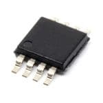
| 产品图片 |
|
| rohs | 符合RoHS无铅 / 符合限制有害物质指令(RoHS)规范要求 |
| 产品系列 | 放大器 IC,电流灵敏放大器,Analog Devices AD8214ARMZ-R7- |
| 数据手册 | |
| 产品型号 | AD8214ARMZ-R7 |
| 产品培训模块 | http://www.digikey.cn/PTM/IndividualPTM.page?site=cn&lang=zhs&ptm=16065 |
| 产品目录页面 | |
| 产品种类 | 电流灵敏放大器 |
| 供应商器件封装 | 8-MSOP |
| 共模抑制比—最小值 | 80 dB |
| 其它名称 | AD8214ARMZ-R7DKR |
| 功能 | 电流监控器 |
| 包装 | Digi-Reel® |
| 商标 | Analog Devices |
| 安装类型 | 表面贴装 |
| 安装风格 | SMD/SMT |
| 封装 | Reel |
| 封装/外壳 | 8-TSSOP,8-MSOP(0.118",3.00mm 宽) |
| 封装/箱体 | MSOP-8 |
| 工作温度 | -40°C ~ 125°C |
| 工厂包装数量 | 1000 |
| 感应方法 | 高端 |
| 拓扑结构 | Current Shunt Feedback |
| 描述/功能 | High CMV threshold detector |
| 最大工作温度 | + 125 C |
| 最小工作温度 | - 40 C |
| 标准包装 | 1 |
| 电压-输入 | 5 V ~ 65 V |
| 电流-输出 | 1mA |
| 电源电压-最大 | 65 V |
| 电源电压-最小 | 5 V |
| 电源电流 | 1.2 mA |
| 精度 | - |
| 系列 | AD8214 |
| 输入电压 | - 0.9 V to + 0.2 V |
| 输入补偿电压 | 3 mV |
| 输出电压 | 2 V to 62.5 V |
| 输出电流 | 1 mA |
| 通道数量 | 1 Channel |


- 商务部:美国ITC正式对集成电路等产品启动337调查
- 曝三星4nm工艺存在良率问题 高通将骁龙8 Gen1或转产台积电
- 太阳诱电将投资9.5亿元在常州建新厂生产MLCC 预计2023年完工
- 英特尔发布欧洲新工厂建设计划 深化IDM 2.0 战略
- 台积电先进制程称霸业界 有大客户加持明年业绩稳了
- 达到5530亿美元!SIA预计今年全球半导体销售额将创下新高
- 英特尔拟将自动驾驶子公司Mobileye上市 估值或超500亿美元
- 三星加码芯片和SET,合并消费电子和移动部门,撤换高东真等 CEO
- 三星电子宣布重大人事变动 还合并消费电子和移动部门
- 海关总署:前11个月进口集成电路产品价值2.52万亿元 增长14.8%


PDF Datasheet 数据手册内容提取
Fast Response, High Voltage Current Shunt Comparator Data Sheet AD8214 FEATURES FUNCTIONAL BLOCK DIAGRAM Input-to-output response: <100 ns VS 1 High input common-mode voltage range Operating: 5 V to 65 V Survival: 0 V to 68 V +IN 2 5 OUT Current output –IN 8 Hysteresis: 10 mV 2.4V REGULATOR Integrated 2.4 V regulator Wide operating temperature range: –40°C to +125°C 8Q-uleaalidfi eMdS fOoPr apuatcokmagoet ive applications VREG 3 6 06193-001 GND APPLICATIONS Figure 1. Overcurrent protection Motor controls Transmission controls Diesel injection controls DC-to-DC converters Power supplies Batteries GENERAL DESCRIPTION The AD8214 is a fast response, high common-mode voltage, The input to output response time of the AD8214 is typically current shunt comparator. The device operates on the high side less than 100 ns. This makes the device optimal for overcurrent rail of any DC current sensing application, provided the voltage protection in applications such as motor and solenoid control. is between 5 V and 65 V. Internally, the AD8214 features a fast Built-in comparator hysteresis means that once the current comparator that is optimized for high side operation. An internal across the shunt falls back to a normal limit, the AD8214 output Zener regulator powers the circuit with respect to the high side will change states to its original level. DC rail. In addition, user access to this 2.4V regulator, allows The AD8214 is available in an 8-lead MSOP package. The for setting a comparator threshold voltage via external resistors. operating temperature range is −40°C to +125°C, and the device The AD8214 will compare the voltage across the shunt resistor is fully qualified for automotive applications. to this user-selected threshold, and the AD8214 output will change states from low to high, indicating the current across the shunt has crossed the threshold level. Rev. A Information furnished by Analog Devices is believed to be accurate and reliable. However, no responsibility is assumed by Analog Devices for its use, nor for any infringements of patents or other One Technology Way, P.O. Box 9106, Norwood, MA 02062-9106, U.S.A. rights of third parties that may result from its use. Specifications subject to change without notice. No license is granted by implication or otherwise under any patent or patent rights of Analog Devices. Tel: 781.329.4700 www.analog.com Trademarks and registered trademarks are the property of their respective owners. Fax: 781.461.3113 ©2006–2012 Analog Devices, Inc. All rights reserved.
AD8214 Data Sheet TABLE OF CONTENTS Features .............................................................................................. 1 Comparator Offset and Hysteresis ........................................... 11 Applications ....................................................................................... 1 Setting the Input Threshold Voltage ........................................ 11 Functional Block Diagram .............................................................. 1 Input-Referred Dynamic Error ................................................ 11 General Description ......................................................................... 1 Applications ..................................................................................... 12 Revision History ............................................................................... 2 Typical Setup and Calculations ................................................ 12 Specifications ..................................................................................... 3 High Side Overcurrent Detection ............................................ 13 Absolute Maximum Ratings ............................................................ 4 Outline Dimensions ....................................................................... 14 ESD Caution .................................................................................. 4 Ordering Guide .......................................................................... 14 Pin Configuration and Function Descriptions ............................. 5 Automotive Products ................................................................. 14 Typical Performance Characteristics ............................................. 6 Theory of Operation ...................................................................... 10 REVISION HISTORY 6/12—Rev. 0 to Rev. A 10/06—Revision 0: Initial Version Changes to Product Title .................................................................. 1 Changes to Features Section, and General Description Section ................................................................................................. 1 Changes to Table 1 ............................................................................. 3 Changes to Table 2 ............................................................................. 4 Changes to Ordering Guide; Added Automotive Products Section ............................................................................................... 14 Updated Outline Dimensions ........................................................ 14 Rev. A | Page 2 of 16
Data Sheet AD8214 SPECIFICATIONS V = 13.5 V, unless otherwise noted. S Table 1. Parameter Conditions/Comments Min Typ Max Unit VOLTAGE OFFSET Offset Voltage (RTI) TA = 25°C, voltage at –IN decreasing ±3 mV Over Temperature (RTI) ±8 mV Offset Drift ±10 µV/°C HYSTERESIS TA = 25°C, voltage at –IN increasing 5 12 mV INPUT Input Impedance Differential 2 MΩ Common Mode V = 5 V to 65 V 5 MΩ S Voltage Range Differential Maximum voltage between +IN and –IN 500 mV Common Mode V – 0.9 V + 0.2 V S S Input Bias Current +IN or –IN 12 ±30 nA OUTPUT Output Current R = 3.3 kΩ, output high 0.8 1 1.2 mA OUT R = 3.3 kΩ, output low ±5 µA OUT Rise Time 20% to 80%, R = 3.3 kΩ, V = 5 mV, 50 mV step 90 ns OUT OD 20% to 80%, ROUT = 3.3 kΩ, VOD = >20 mV, 50 mV step 75 ns Fall Time 20% to 80%, R = 3.3 kΩ, V = 5 mV, 50 mV step 110 ns OUT OD 20% to 80%, ROUT = 3.3 kΩ, VOD = >10 mV, 50 mV step 100 ns REGULATOR Nominal Value TA = 25°C, voltage from VREG to VS 2.43 V TA = –40°C to +125°C ±5 % DYNAMIC RESPONSE 50 mV to 250 mV step Propagation Delay1 5 mV ≤ V ≤ 15 mV, output low to high 90 ns OD 15 mV ≤ V ≤ 30 mV, output low to high 80 ns OD V ≥ 30 mV, output low to high 75 ns OD INPUT-REFERRED DYNAMIC ERROR2 15 mV POWER SUPPLY Operating Range Maximum Voltage GND to V 65 V S Minimum Voltage GND to V 5 V S Output Voltage Range3 With respect to V 2 62.5 V REG Supply Current Output low 240 µA Output high 1.2 mA TEMPERATURE RANGE FOR SPECIFIED PERFORMANCE −40 +125 °C 1 VOD represents the overdrive voltage, or the amount of voltage by which the threshold point has been exceeded. 2 See the Input-Referred Dynamic Error section. 3 The voltage at OUT must not be allowed to exceed the VREG voltage, which is always 2.4 V less than the supply. For example, when the supply voltage is 5 V and the output current is 1 mA, the load resistor must not be more than (5 V – 2.4 V)/{1 mA × (1 + 20%)}, or 2.17 kΩ, to ensure the signal does not exceed 2.6 V. As the supply increases, the output signal also can be increased, by the same amount. Rev. A | Page 3 of 16
AD8214 Data Sheet ABSOLUTE MAXIMUM RATINGS T = –40°C to +125°C A Table 2. ESD CAUTION Parameter Rating Supply Voltage 65 V Continuous Input Voltage 68 V Differential Input Voltage 500 mV Reverse Supply Voltage 0.3 V Operating Temperature Range −40°C to +125°C Storage Temperature Range −65°C to +150°C Output Short-Circuit Duration Indefinite Stresses above those listed under Absolute Maximum Ratings may cause permanent damage to the device. This is a stress rating only; functional operation of the device at these or any other conditions above those indicated in the operational section of this specification is not implied. Exposure to absolute maximum rating conditions for extended periods may affect device reliability. Rev. A | Page 4 of 16
Data Sheet AD8214 PIN CONFIGURATION AND FUNCTION DESCRIPTIONS 1 6 8 VS 1 AD8214 8 –IN 2 +IN 2 TOP VIEW 7 NC VREG 3 (Not to Scale) 6 GND 3 5 06193-007 NC N4C = NO CONNECT5 OUT 06193-002 Figure 2. Metallization Diagram Figure 3. Pin Configuration Table 3. Pin Function Descriptions Pin No. Mnemonic X Y Description 1 V –196 +447 Supply Voltage. S 2 +IN –198 –58 Noninverting Input. 3 V –196 –346 Regulator Voltage. REG 4 NC No Connect. 5 OUT +196 –348 Output. 6 GND +196 +447 Ground. 7 NC No Connect. 8 –IN –31 +449 Inverting Input. Rev. A | Page 5 of 16
AD8214 Data Sheet TYPICAL PERFORMANCE CHARACTERISTICS 16 0 15 V) –0.4 T (nA) 14 GE (m REN 5V LTA –0.8 R O U V C 13 T UT BIAS 12 65V T OFFSE –1.2 P U N P I N I –1.6 11 10 06193-041 –2.0 06193-035 –1.2 –1.0 –0.8 –0.6 –0.4 –0.2 0 0.2 –0.9 –0.8 –0.7 –0.6 –0.5 –0.4 –0.3 –0.2 –0.1 0 0.1 0.2 INPUT COMMON-MODE VOLTAGE (V) INPUT COMMON-MODE VOLTAGE (V) Figure 4. Input Bias Current vs. Input Common-Mode Voltage Figure 7. Input Offset Voltage vs. Input Common-Mode Voltage (With Respect to VS) (With Respect to VS) 280 1.11 1.09 270 TA = –40°C T (mA) 1.07 T (µA) 260 N N E E URR 1.05 URR 250 TA = +25°C C C UT 1.03 LY TP PP 240 TA = +125°C U U O 1.01 S 230 00..9979 06193-024 220 06193-023 –1.40 –1.15 –0.90 –0.65 –0.40 –0.15 0.10 5 15 25 35 45 55 65 INPUT COMMON-MODE VOLTAGE (V) SUPPLY VOLTAGE (V) Figure 5. Output Current (Output High) vs. Input Common-Mode Voltage Figure 8. Supply Current vs. Supply Voltage (With Respect to VS) (Output Low) 4 1.25 1.24 TA = –40°C V) ET VOLTAGE (m 02 CURRENT (mA) 11..2223 TA = +25°C UT OFFS SUPPLY 11..2201 TA = +125°C P –2 N I –4 06193-018 11..1189 06193-034 –40 –25 –10 5 20 35 50 65 80 95 110 125 5 15 25 35 45 55 65 TEMPERATURE (°C) SUPPLY VOLTAGE (V) Figure 6. Input Offset Voltage vs. Temperature Figure 9. Supply Current vs. Supply Voltage (Output High) Rev. A | Page 6 of 16
Data Sheet AD8214 2.448 1.10 2.444 TA = +125°C E (V) mA) 1.05 OLTAG 2.440 TA = +125°C RENT ( TA = +25°C R V UR 1.00 O C AT 2.436 UT TA = –40°C GUL TA = +25°C UTP E O R 0.95 2.432 TA = –40°C 2.428 06193-022 0.90 06193-020 5 15 25 35 45 55 65 5 15 25 35 45 55 65 SUPPLY VOLTAGE (V) SUPPLY VOLTAGE (V) Figure 10. Regulator Voltage vs. Supply Voltage Figure 13. Output Current vs. Supply Voltage (Between VREG and VS) (Output High) 2.50 12.0 11.5 GE (V) 2.45 TA = +125°C TA = +25°C E (mV) 11.0 TA AG 10.5 L T O L TOR V 2.40 TA = –40°C SIS VO 10.0 A E L R 9.5 U E G T E S R 2.35 HY 9.0 2.30 06193-021 88..05 06193-017 10 50 100 150 200 –40 –25 –10 5 20 35 50 65 80 95 110 125 REGULATOR LOAD RESISTANCE (kΩ) TEMPERATURE (°C) Figure 11. Regulator Voltage vs. Regulator Load Resistance Figure 14. Hysteresis Voltage vs. Temperature (Series Resistance Between VREG and VS) (–IN Increasing) 700 170 ROUT = 5kΩ TA = +125°C 600 150 A) 500 T (n s) 130 N n T CURRE 340000 LL TIME ( 110 ROUT = 3.3kΩ U A P F T 90 U O 200 TA = +25°C 70 1000 TA = –40°C 06193-019 50 06193-027 5 15 25 35 45 55 65 15 25 35 45 55 65 75 85 95 SUPPLY VOLTAGE (V) OVERDRIVE VOLTAGE (mV) Figure 12. Output Current vs. Supply Voltage Figure 15. Fall Time vs. Overdrive Voltage (Output Low) (–IN > +IN by Specified VOD) Rev. A | Page 7 of 16
AD8214 Data Sheet 110 –IN 30mV/DIV 90 ROUT = 5kΩ VOD = 50mV +IN s) n E ( M E TI ROUT = 3.3kΩ RIS VOD = 30mV 70 OUT 2V/DIV 505 15 25 35 45 55 65 75 85 95 06193-028 06193-031 OVERDRIVE VOLTAGE (mV) 100ns/DIV Figure 16. Rise Time vs. Overdrive Voltage Figure 19. Typical Propagation Delay (ROUT = 5 kΩ) (+IN > –IN by Specified VOD) –IN 10mV/DIV VOD = 100mV +IN VOD = 15mV +IN –IN 50mV/DIV VOD = 5mV VOD = 100mV OUT 2V/DIV OUT 2V/DIV 06193-029 06193-032 100ns/DIV 100ns/DIV Figure 17. Typical Propagation Delay (ROUT = 5 kΩ) Figure 20. Typical Propagation Delay (ROUT = 5 kΩ) –IN 190 10mV/DIV 170 +IN ns) VOD = 20mV AY ( 150 L E D N 130 O TI A VOD = 10mV AG 110 ROUT = 5kΩ P OUT O 2V/DIV R 90 P 06193-030 570015 25 35 45 RO5U5T = 3.635kΩ 75 85 95 06193-026 100ns/DIV OVERDRIVE VOLTAGE (mV) Figure 18. Typical Propagation Delay (ROUT = 5 kΩ) Figure 21. Propagation Delay vs. Overdrive Voltage (–IN > +IN by Specified VOD, Output High to Low) Rev. A | Page 8 of 16
Data Sheet AD8214 120 240 MEAN = –10 210 110 s) 180 n ELAY ( 100 ROUT = 3.3kΩ 150 D T ON 90 OUN 120 TI C A AG 90 P 80 PRO ROUT = 5kΩ 60 70 60 06193-025 300 06193-040 5 15 25 35 45 55 65 75 85 95 –12.0 –11.5 –11.0 –10.5 –10.0 –9.5 –9.0 –8.5 –8.0 OVERDRIVE VOLTAGE (mV) HYSTERESIS VOLTAGE (mV) Figure 22. Propagation Delay vs. Overdrive Voltage, Figure 25. Hysteresis Voltage Distribution (+IN > –IN by Specified VOD, Output Low to High) 12 240 MEAN = 987.7 210 V) 11 m E ( 180 G OLTA 10 UNT 150 S V CO 120 SI E 9 R 90 E T S Y 60 H 8 7–1.0 –0.9 –0.8 –0.7 –0.6 –0.5 –0.4 –0.3 –0.2 –0.1 0 0.1 0.206193-037 300800 850 900 950 1000 1050 1100 1150 120006193-039 INPUT COMMON-MODE VOLTAGE (V) OUTPUT CURRENT (µA) Figure 23. Hysteresis Voltage vs. Input Common-Mode Voltage Figure 26. Output Current Distribution (With Respect to VS) 140 160 MEAN = –0.16 MEAN = –2.42 140 120 120 100 100 T 80 T N N U U 80 O O C 60 C 60 40 40 200 06193-036 200 06193-038 –4 –3 –2 –1 0 1 2 3 4 –2.46 –2.45 –2.44 –2.43 –2.42 –2.41 –2.40 INPUT OFFSET VOLTAGE (mV) REGULATOR VOLTAGE (V) Figure 24. Input Offset Voltage Distribution Figure 27. Regulator Voltage Distribution (With Respect to VS) Rev. A | Page 9 of 16
AD8214 Data Sheet THEORY OF OPERATION The AD8214 is a high voltage comparator offering an input-to- connects to a voltage divider across the regulator, so the output response time of less than 100 ns. This device is ideal for comparator trips as the voltage across the series resistor crosses detecting overcurrent conditions on the high side of the control the user-selected threshold. loop. The AD8214 is designed specifically to facilitate and allow The AD8214 features a current output. The current is low (100 nA for fast shutdown of the control loop, preventing damage due to typical), until the user selected threshold is crossed. After this point excessive currents to the FET, load, or shunt resistor. the output switches to high (1 mA typical). The current output The AD8214 operates with a supply of 5 V to 65 V. It combines driver complies with load voltage from 0 V to (V – 2.4 V). The S a fast comparator, optimized for high side operation, with a current easily drives a ground referenced resistor to develop logic 2.4 V series voltage regulator. The regulator provides a stable levels determined by the value of the load resistor. voltage that is negative with respect to the positive supply rail, The comparator input is balanced to switch as the inverting and it is intended to provide power to the internal electronics, input (–IN) is driven negative with respect to the noninverting set a comparison threshold below the supply rail, and power input (+IN). As the comparator output switches from 0 mA to small application circuits used with the comparator. 1 mA, a small hysteresis (10 mV) is activated to minimize the The differential input of the comparator may be operated at, or effects of noise in the system that may be triggered by the slightly above or below, the positive supply rail. Typically, one of comparator signal. This means that to restore the output to zero, the comparator inputs is driven negative with respect to the the input polarity must be reversed by 10 mV beyond the positive supply by a small series resistor carrying the main original threshold. supply current to the load. The other input of the comparator BATTERY CONSTANT THRESHOLD I 1 1 + R1 _ 2 + SHUNT 5 UP TO 65V _ 8 CONSTANT VAOCRLTOASGSE S DHRUONTP R2 REGU2L.4AVTOR 2.4V CORRESPONDING TO CURRENT LEVEL TO LOAD 3 2 6 3 06193-005 Figure 28. Simplified Schematic Rev. A | Page 10 of 16
Data Sheet AD8214 COMPARATOR OFFSET AND HYSTERESIS values for these resistors can be chosen based on the desired threshold voltage using the equation: The AD8214 features built-in hysteresis to minimize the effects of noise in the system. There is also a small offset at the input of 2.4 × R1 = VTH(+IN) (1) the device. R1+R2 For proper operation it is recommended that the internal 2.4 V regulator not be loaded down by using small R1 and R2 values. VOH Figure 11 shows the proper range for the total series resistance. INPUT-REFERRED DYNAMIC ERROR VH Frequently, the dynamics of comparators are specified in terms of propagation delay of the response at the output to an input VOL VOS pulse crossing the threshold between two overload states. For VVOH S= =H IYNSPTUETR OEFSFISS EVTO LVTOALGTEAGE VTH 06193-033 tchoims mpaeraesdu troe mtheen ct,o tmhep arrisaet otrim preo opfa tghaet iionnp udte lpauy.l sIen i tsh nee cgalisgei bolfe VTH = THRESHOLD VOLTAGE the AD8214, this propagation delay is typically 100 ns, when the VOH = OUTPUT HIGH VOL = OUTPUT LOW input signal is a fast step. Figure 29. Hysteresis and Input Offset Voltage Definition The primary purpose of the AD8214 is to monitor for over- current conditions in a system. It is much more common that in Figure 29 shows the relationship between the input voltage and the such systems, the current in the path increases slowly; therefore, output current. The horizontal axis represents the voltage between the transition between two input overload conditions around the positive (+IN) and negative (–IN) inputs of the AD8214. The the threshold is slow relative to the propagation delay. In some vertical axis shows the output current for a given input voltage. cases, this transition can be so slow that the time from the V represents the point where the inputs are at the same voltage TH actual threshold crossing to the output signal switching states is level (+IN = –IN). The output of the AD8214 remains low (V ) OL longer than the specified propagation delay, due to the provided (–IN) is at a higher voltage potential than (+IN). As the comparator dynamics. input voltage transitions to +IN > –IN, the output switches states. If the voltage at the input of the AD8214 is crossing the set Under ideal conditions, the output is expected to change states at threshold at a rate ≤100 mV/µs, the output switches states exactly V . In practice, the output switches when the inputs are TH before the threshold voltage has been exceeded by 15 mV. equal ± a small offset voltage (V ). OS Therefore, if the input signal is changing so slowly that the Once the output switches from low to high, it remains in this state propagation delay is affected, the error that accumulates at the until the input voltage falls below the hysteresis voltage. Typically, input while waiting for the output response is proportionately this occurs when +IN is 10 mV below –IN. smaller and, typically, less than 15 mV for ramp rates SETTING THE INPUT THRESHOLD VOLTAGE ≤100 mV/µs. The AD8214 features a 2.4 V series regulator, which can be used to set a reference threshold voltage with two external resistors. The resistors constitute a voltage divider, the middle point of which connects to +IN. The total voltage across the resistors is always 2.4 V. (See Figure 28 for proper resistor placement.) The Rev. A | Page 11 of 16
AD8214 Data Sheet APPLICATIONS TYPICAL SETUP AND CALCULATIONS Under normal operating conditions, the current is 10 A or less, corresponding to a maximum voltage drop across the shunt of The key feature of the AD8214 is its ability to detect an overcurrent 50 mV. This means that the negative input of the comparator is condition on the high side of the rail and provide a signal in less 50 mV below the battery voltage. Since the positive input is than 100 ns. This performance protects expensive loads, FETs, and 75 mV below the battery voltage, the negative input is at a shunt resistors in a variety of systems and applications. This section higher potential than the positive; therefore, the output of the details a typical application in which the normal current in the AD8214 is low. system is less ≤10 A and an overcurrent detection is necessary If the current increases to 15 A, the drop across the shunt is when 15 A is detected in the path. 75 mV. As the current continues to increase, the positive input If we assume a shunt resistance (R ) of 0.005 Ω and a SHUNT of the comparator reaches a higher potential than the negative, common-mode voltage range of 5 V to 65 V, the typical voltage and the output of the AD8214 switches from low to high. The across the shunt resistor is input-to-output response of the AD8214 is less than 100 ns. The 10 A × 0.005 Ω = 50 mV output resistor in this case is selected so that the logic level high signal is 3.3 V. The voltage drop across the shunt resistor, in the case of an overcurrent condition is The output changes states from low to high in the case of an overcurrent condition. However, the input offset voltage is 15 A × 0.005 Ω = 75 mV typically 1 mV; therefore, this must be taken into consideration The threshold voltage, must therefore be set at 75 mV, when choosing the threshold voltage. When the current in the corresponding to the overcurrent condition. R1 and R2 can be system drops back down to normal levels, the AD8214 changes selected based on this 75 mV threshold at the positive input of states from high to low. However, due to the built-in 10 mV the comparator. hysteresis, the voltage at (–IN) must be 10 mV higher than the A low load current across the regulator corresponds to optimal threshold for the output to change states from high to low. This regulator performance; therefore, the series resistance of R1 and built-in hysteresis is intended to prevent input chatter as well as R2 must be relatively large. For this case, the total resistance can any false states. be set as Table 4 shows typical resistors combinations that can be used to set R1 + R2 = 200 kΩ an input threshold voltage. Numbers are based on a 2.43 V V . REG To have a 75 mV drop across R1, the following calculations apply: Table 4. 2.4V Threshold (mV) R1 (kΩ) R2 (kΩ) = 12 µA 200 kΩ 30 1.5 120 50 1.6 75 75 mV = 6.25 kΩ = R1 60 2 80 12 µA 75 2.4 75 R2 = (200 kΩ – R1) = 193.75 kΩ 110 8.06 169 The values for R1 and R2 are set; correspondingly, the threshold voltage at +IN is set at 75 mV. BATTERY 1 I C1 R1 0.01µF 6.25kΩ RSHUNT 2 5 IOUT (0.005Ω) 8 ILOAD 193.75kRΩ2 REGU2L.4AVTOR ROUT=V 3O.3UkTΩ 3 6 06193-006 Figure 30. Typical Application Rev. A | Page 12 of 16
Data Sheet AD8214 HIGH SIDE OVERCURRENT DETECTION reaches an undesirable level that corresponds to the user-selected threshold, the output of the AD8214 switches states in less than The AD8214 is useful for many automotive applications using the 100 ns. The microcontroller, analog-to-digital converter, or FET load configuration shown in Figure 31. Because the part powers driver can be directly notified of this condition. directly from the battery voltage, the shunt resistor must be on the high side. The AD8214 monitors the current in the path as long as the battery voltage is between 5 V and 65 V. If the current I SHUNT BATTERY CLAMP UP TO 65V DIODE SWITCH AD8214 1 VS –IN 8 C1 R1 2 +IN NC 7 R2 3 VREG GND 6 4 NC OUT 5 ODEVTEERCCTUIRORNE (N<1T00ns) 06193-004 Figure 31. High Side Overcurrent Protection Rev. A | Page 13 of 16
AD8214 Data Sheet OUTLINE DIMENSIONS 3.20 3.00 2.80 8 5 5.15 3.20 4.90 3.00 4.65 2.80 1 4 PIN1 IDENTIFIER 0.65BSC 0.95 15°MAX 0.85 1.10MAX 0.75 0.80 0.15 0.40 6° 0.23 0.55 CO0P.0L50A.1N0ARICTOYMPLIANT0.T25OJEDECSTA0°NDARDS0M.0O9-187-AA 0.40 10-07-2009-B Figure 32. 8-Lead Mini Small Outline Package [MSOP] (RM-8) Dimensions shown in millimeters ORDERING GUIDE Model1, 2 Temperature Range Package Description Package Option Branding AD8214ARMZ −40°C to +125°C 8-Lead MSOP RM-8 H0N AD8214ARMZ-RL −40°C to +125°C 8-Lead MSOP, 13” Tape and Reel RM-8 H0N AD8214ARMZ-R7 −40°C to +125°C 8-Lead MSOP, 7” Tape and Reel RM-8 H0N AD8214WYRMZ −40°C to +125°C 8-Lead MSOP RM-8 Y2E AD8214WYRMZ-RL −40°C to +125°C 8-Lead MSOP, 13” Tape and Reel RM-8 Y2E AD8214WYRMZ-R7 −40°C to +125°C 8-Lead MSOP, 7” Tape and Reel RM-8 Y2E 1 Z = RoHS Compliant Part. 2 W = Qualified for Automotive Applications. AUTOMOTIVE PRODUCTS The AD8214W models are available with controlled manufacturing to support the quality and reliability requirements of automotive applications. Note that these automotive models may have specifications that differ from the commercial models; therefore, designers should review the Specifications section of this data sheet carefully. Only the automotive grade products shown are available for use in automotive applications. Contact your local Analog Devices account representative for specific product ordering information and to obtain the specific Automotive Reliability reports for these models. Rev. A | Page 14 of 16
Data Sheet AD8214 NOTES Rev. A | Page 15 of 16
AD8214 Data Sheet NOTES ©2006–2012 Analog Devices, Inc. All rights reserved. Trademarks and registered trademarks are the property of their respective owners. D06193-0-6/12(A) Rev. A | Page 16 of 16
Mouser Electronics Authorized Distributor Click to View Pricing, Inventory, Delivery & Lifecycle Information: A nalog Devices Inc.: AD8214ARMZ AD8214ARMZ-R7 AD8214ARMZ-RL AD8214WYRMZ AD8214WYRMZ-R7 AD8214WYRMZ-RL