ICGOO在线商城 > 集成电路(IC) > PMIC - 稳流/电流管理 > AD8210YRZ-REEL7
 Datasheet下载
- 型号: AD8210YRZ-REEL7
- 制造商: Analog
- 库位|库存: xxxx|xxxx
- 要求:
| 数量阶梯 | 香港交货 | 国内含税 |
| +xxxx | $xxxx | ¥xxxx |
查看当月历史价格
查看今年历史价格
AD8210YRZ-REEL7产品简介:
ICGOO电子元器件商城为您提供AD8210YRZ-REEL7由Analog设计生产,在icgoo商城现货销售,并且可以通过原厂、代理商等渠道进行代购。 AD8210YRZ-REEL7价格参考¥28.04-¥44.79。AnalogAD8210YRZ-REEL7封装/规格:PMIC - 稳流/电流管理, Current Monitor Regulator High/Low-Side 5mA 8-SOIC。您可以下载AD8210YRZ-REEL7参考资料、Datasheet数据手册功能说明书,资料中有AD8210YRZ-REEL7 详细功能的应用电路图电压和使用方法及教程。
AD8210YRZ-REEL7是Analog Devices Inc.推出的一款高精度电流检测放大器,属于PMIC - 稳流/电流管理类别。该器件主要用于对电流信号进行精确采集和放大,广泛应用于需要实时监测电流的工业与汽车电子系统。

典型应用场景包括:电机控制、电源管理系统、电池供电设备、过流保护电路以及车载应用如电动车窗、电动座椅和发动机控制模块等。AD8210YRZ-REEL7具有宽输入共模电压范围(-2 V至+65 V),可在高压环境中稳定工作,适合在48V汽车电气系统或工业电源中使用。其高抗噪能力和出色的直流精度使其在恶劣电磁环境下仍能保持可靠性能。

此外,该器件采用小尺寸SOIC封装,便于集成到紧凑型电路板中,适用于空间受限的设计。因其具备高可靠性与温度稳定性,也常用于工业自动化设备中的电流反馈回路和可再生能源系统(如太阳能逆变器)中的电流监控模块。

综上,AD8210YRZ-REEL7是一款适用于汽车电子、工业控制和电源管理等领域中高精度、高可靠性电流检测需求的理想选择。
| 参数 | 数值 |
| 产品目录 | 集成电路 (IC)半导体 |
| 描述 | IC CURRENT MONITOR 0.5% 8SOIC电流灵敏放大器 High Voltage Bidirectional |
| 产品分类 | |
| 品牌 | Analog Devices Inc |
| 产品手册 | |
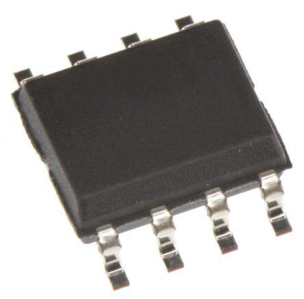
| 产品图片 |
|
| rohs | 符合RoHS无铅 / 符合限制有害物质指令(RoHS)规范要求 |
| 产品系列 | 放大器 IC,电流灵敏放大器,Analog Devices AD8210YRZ-REEL7- |
| 数据手册 | |
| 产品型号 | AD8210YRZ-REEL7 |
| 产品种类 | 电流灵敏放大器 |
| 供应商器件封装 | 8-SOIC |
| 共模抑制比—最小值 | 100 dB |
| 其它名称 | AD8210YRZ-REEL7DKR |
| 功能 | 电流监控器 |
| 包装 | Digi-Reel® |
| 商标 | Analog Devices |
| 安装类型 | 表面贴装 |
| 安装风格 | SMD/SMT |
| 封装 | Reel |
| 封装/外壳 | 8-SOIC(0.154",3.90mm 宽) |
| 封装/箱体 | SOIC-8 |
| 工作温度 | -40°C ~ 125°C |
| 工厂包装数量 | 1000 |
| 带宽 | 500 kHz |
| 感应方法 | 高/低端 |
| 拓扑结构 | Current Shunt Feedback |
| 描述/功能 | Bidirectional shunt monitor |
| 最大工作温度 | + 125 C |
| 最小工作温度 | - 40 C |
| 标准包装 | 1 |
| 电压-输入 | -2 V ~ 65 V |
| 电压增益dB | 26.02 dB |
| 电流-输出 | 5mA |
| 电源电压-最大 | 5.5 V |
| 电源电压-最小 | 4.5 V |
| 电源电流 | 1.5 mA |
| 精度 | ±0.7% |
| 系列 | AD8210 |
| 设计资源 | |
| 输入补偿电压 | 1000 uV |
| 通道数量 | 1 Channel |


- 商务部:美国ITC正式对集成电路等产品启动337调查
- 曝三星4nm工艺存在良率问题 高通将骁龙8 Gen1或转产台积电
- 太阳诱电将投资9.5亿元在常州建新厂生产MLCC 预计2023年完工
- 英特尔发布欧洲新工厂建设计划 深化IDM 2.0 战略
- 台积电先进制程称霸业界 有大客户加持明年业绩稳了
- 达到5530亿美元!SIA预计今年全球半导体销售额将创下新高
- 英特尔拟将自动驾驶子公司Mobileye上市 估值或超500亿美元
- 三星加码芯片和SET,合并消费电子和移动部门,撤换高东真等 CEO
- 三星电子宣布重大人事变动 还合并消费电子和移动部门
- 海关总署:前11个月进口集成电路产品价值2.52万亿元 增长14.8%


PDF Datasheet 数据手册内容提取
High Voltage, Bidirectional Current Shunt Monitor Data Sheet AD8210 FEATURES FUNCTIONAL BLOCK DIAGRAM ±4000 V HBM ESD VSUPPLY IS High common-mode voltage range −2 V to +65 V operating RS −5 V to +68 V survival Buffered output voltage +IN –IN V+ 5 mA output drive capability VS Wide operating temperature range: −40°C to +125°C Ratiometric half-scale output offset AD8210 Excellent ac and dc performance LOAD 1 µV/°C typical offset drift 10 ppm/°C typical gain drift VREF1 120 dB typical CMRR at dc 80 dB typical CMRR at 100 kHz Available in 8-lead SOIC G=+20 VOUT Qualified for automotive applications APPLICATIONS VREF2 Current sensing Motor controls GND TDriaensesml inisjseicotnio cno ncotrnotlrso ls 05147-001 Engine management Figure 1. Suspension controls Vehicle dynamic controls DC-to-dc converters GENERAL DESCRIPTION The AD8210 is a single-supply, difference amplifier ideal for The output offset can be adjusted from 0.05 V to 4.9 V with amplifying small differential voltages in the presence of large a 5 V supply by using the V 1 pin and the V 2 pin. With the REF REF common-mode voltages. The operating input common-mode V 1 pin attached to the V+ pin and the V 2 pin attached to REF REF voltage range extends from −2 V to +65 V. The typical supply the GND pin, the output is set at half scale. Attaching both V 1 REF voltage is 5 V. and V 2 to GND causes the output to be unipolar, starting REF near ground. Attaching both V 1 and V 2 to V+ causes the The AD8210 is offered in a SOIC package. The operating REF REF output to be unipolar, starting near V+. Other offsets can be temperature range is −40°C to +125°C. obtained by applying an external voltage to V 1 and V 2. REF REF Excellent ac and dc performance over temperature keep errors in the measurement loop to a minimum. Offset drift and gain drift are guaranteed to a maximum of 8 µV/°C and 20 ppm/°C, respectively. Rev. E Document Feedback Information furnished by Analog Devices is believed to be accurate and reliable. However, no responsibility is assumed by Analog Devices for its use, nor for any infringements of patents or other One Technology Way, P.O. Box 9106, Norwood, MA 02062-9106, U.S.A. rights of third parties that may result from its use. Specifications subject to change without notice. No license is granted by implication or otherwise under any patent or patent rights of Analog Devices. Tel: 781.329.4700 ©2006–2017 Analog Devices, Inc. All rights reserved. Trademarks and registered trademarks are the property of their respective owners. Technical Support www.analog.com
AD8210 Data Sheet TABLE OF CONTENTS Features .............................................................................................. 1 Modes of Operation ....................................................................... 11 Applications ....................................................................................... 1 Unidirectional Operation .......................................................... 11 Functional Block Diagram .............................................................. 1 Bidirectional Operation ............................................................. 11 General Description ......................................................................... 1 Input Filtering ................................................................................. 13 Revision History ............................................................................... 2 Applications Information .............................................................. 14 Specifications ..................................................................................... 3 High-Side Current Sense with a Low-Side Switch ................. 14 Absolute Maximum Ratings ............................................................ 4 High-Side Current Sense with a High-Side Switch ............... 14 ESD Caution .................................................................................. 4 H-Bridge Motor Control ........................................................... 14 Pin Configuration and Function Descriptions ............................. 5 Outline Dimensions ....................................................................... 15 Typical Performance Characteristics ............................................. 6 Ordering Guide .......................................................................... 15 Theory of Operation ...................................................................... 10 Automotive Products ................................................................. 15 REVISION HISTORY 9/2017—Rev. D to Rev. E 5/2009—Rev. A to Rev. B Change to Ordering Guide ............................................................ 15 Changes to Ordering Guide .......................................................... 15 6/2013—Rev. C to Rev. D 4/07—Rev. 0 to Rev. A Added Automotive Information (Throughout) ........................... 1 Changes to Features .......................................................................... 1 Changes to Equation 1 ................................................................... 13 Changes to Input Section ................................................................. 3 Added Automotive Products Section .......................................... 15 Updated Outline Dimensions ....................................................... 15 2/2012—Rev. B to Rev. C 4/2006—Revision 0: Initial Version Changes to Ordering Guide .......................................................... 15 Rev. E | Page 2 of 15
Data Sheet AD8210 SPECIFICATIONS T = operating temperature range, V = 5 V, unless otherwise noted. A S Table 1. AD8210 SOIC1 Parameter Min Typ Max Unit Conditions GAIN Initial 20 V/V Accuracy ±0.5 % 25°C, V ≥ 0.1 V dc O Accuracy Over Temperature ±0.7 % T A Gain Drift 20 ppm/°C VOLTAGE OFFSET Offset Voltage (RTI) ±1.0 mV 25°C Over Temperature (RTI) ±1.8 mV T A Offset Drift ±8.0 µV/°C INPUT Input Impedance Differential 2 kΩ Common Mode 5 MΩ V common mode > 5 V 1.5 kΩ V common mode < 5 V Common-Mode Input Voltage Range −2 +65 V Common mode, continuous Differential Input Voltage Range 250 mV Differential2 Common-Mode Rejection 100 120 dB T , f = dc, V > 5 V A CM 80 95 dB T , f = dc to 100 kHz3, V < 5 V A CM 80 dB T , f = 100 kHz3, V > 5 V A CM 80 dB T , f = 40 kHz3, V > 5 V A CM OUTPUT Output Voltage Range 0.05 4.9 V R = 25 kΩ L Output Impedance 2 Ω DYNAMIC RESPONSE Small Signal −3 dB Bandwidth 450 kHz Slew Rate 3 V/µs NOISE 0.1 Hz to 10 Hz, RTI 7 µV p-p Spectral Density, 1 kHz, RTI 70 nV/√Hz OFFSET ADJUSTMENT Ratiometric Accuracy4 0.499 0.501 V/V Divider to supplies Accuracy, RTO ±0.6 mV/V Voltage applied to V 1 and V 2 in parallel REF REF Output Offset Adjustment Range 0.05 4.9 V V = 5 V S V Input Voltage Range 0.0 V V REF S V Divider Resistor Values 24 32 40 kΩ REF POWER SUPPLY, V S Operating Range 4.5 5.0 5.5 V Quiescent Current Over Temperature 2 mA V > 5 V5 CM Power Supply Rejection Ratio 80 dB TEMPERATURE RANGE For Specified Performance −40 +125 °C 1 TMIN to TMAX = −40°C to +125°C. 2 Differential input voltage range = ±125 mV with half-scale output offset. 3 Source imbalance < 2 Ω. 4 The offset adjustment is ratiometric to the power supply when VREF1 and VREF2 are used as a divider between the supplies. 5 When the input common mode is less than 5 V, the supply current increases. This can be calculated with the following formula: IS = −0.7 (VCM) + 4.2 (see Figure 21). Rev. E | Page 3 of 15
AD8210 Data Sheet ABSOLUTE MAXIMUM RATINGS Stresses at or above those listed under Absolute Maximum Table 2. Ratings may cause permanent damage to the product. This is a Parameter Rating stress rating only; functional operation of the product at these Supply Voltage 12.5 V or any other conditions above those indicated in the operational Continuous Input Voltage (V ) −5 V to +68 V CM section of this specification is not implied. Operation beyond Reverse Supply Voltage 0.3 V the maximum operating conditions for extended periods may ESD Rating affect product reliability. HBM (Human Body Model) ±4000 V CDM (Charged Device Model) ±1000 V Operating Temperature Range −40°C to +125°C ESD CAUTION Storage Temperature Range −65°C to +150°C Output Short-Circuit Duration Indefinite Rev. E | Page 4 of 15
Data Sheet AD8210 PIN CONFIGURATION AND FUNCTION DESCRIPTIONS –IN 1 8 +IN GND 2 AD8210 7 VREF1 VREF2 3 TOPVIEW 6 V+ NC N4C(=NoNtOtoCSOcNaNleE)CT5 OUT 05147-003 Figure 2. Pin Configuration 1 8 2 7 6 3 5 05147-002 Figure 3. Metallization Diagram Table 3. Pin Function Descriptions Pin No. Mnemonic X Y 1 −IN −443 +584 2 GND −479 +428 3 V 2 −466 −469 REF 4 NC 5 OUT +466 −537 6 V+ +501 −95 7 V 1 +475 +477 REF 8 +IN +443 +584 Rev. E | Page 5 of 15
AD8210 Data Sheet TYPICAL PERFORMANCE CHARACTERISTICS 200 2000 180 160 1600 140 120 1200 100 80 m) 800 60 p V (µV)OSI ––244200000 N ERROR (p–4400000 –60 AI G –80 –800 –100 –120 –1200 –140 –160 –1600 –180 –200 –2000 –40–30–20–10 0 10 T2E0M3P0ER4A0TU50RE6(0°C7)0 80 90100110120 05147-030 –40–30–20–10 0 10 T2E0M3P0ER4A0TU50RE6 (0°C7)0 80 90100110120 05147-033 Figure 4. Typical Offset Drift Figure 7. Typical Gain Drift 140 30 25 130 20 15 120 10 5 110 0 CMRR (dB) 100 +125°C +25°C GAIN (dB) ––11–055 90 –20 –40°C –25 80 –30 –35 70 –40 –45 60 –50 100 1kFREQUENCY(Hz)10k 100k 05147-032 10 100 1kFREQU1E0NkCY(Hz)100k 1M 10M 05147-014 Figure 5. CMRR vs. Frequency and Temperature Figure 8. Typical Small Signal Bandwidth (VOUT = 200 mV p-p) (Common-Mode Voltage < 5 V) 140 100mV/DIV 130 +25°C 120 500mV/DIV 110 dB) –40°C +125°C R ( 100 R M C 90 80 70 60100 1kFREQUENCY(Hz)10k 100k 05147-031 400ns/DIV 05147-017 Figure 6. CMRR vs. Frequency and Temperature Figure 9. Fall Time (Common-Mode Voltage > 5 V) Rev. E | Page 6 of 15
Data Sheet AD8210 4V/DIV 100mV/DIV 0.02%/DIV 500mV/DIV 400ns/DIV 05147-018 4µs/DIV 05147-024 Figure 10. Rise Time Figure 13. Settling Time (Falling) 200mV/DIV 4V/DIV 0.02%/DIV 2V/DIV 1µs/DIV 05147-016 4µs/DIV 05147-025 Figure 11. Differential Overload Recovery (Falling) Figure 14. Settling Time (Rising) 50V/DIV 200mV/DIV 2V/DIV 100mV/DIV 1µs/DIV 05147-015 1µs/DIV 05147-019 Figure 12. Differential Overload Recovery (Rising) Figure 15. Common-Mode Response (Falling) Rev. E | Page 7 of 15
AD8210 Data Sheet 5.0 4.9 4.8 50V/DIV V) 4.7 E ( 4.6 G N 4.5 A E R 4.4 100mV/DIV AG 4.3 LT 4.2 O V 4.1 UT 4.0 P T 3.9 U O 3.8 3.7 3.6 1µs/DIV 05147-020 3.50 0.5 1.0 1.O5UT2P.0UT2S.5OU3R.0CE3C.5UR4R.0ENT4.(5mA5).0 5.5 6.0 6.5 05147-023 Figure 16. Common-Mode Response (Rising) Figure 19. Output Voltage Range vs. Output Source Current 8 1.4 mA) 7 D (V) 1.2 T ( GN REN 6 OM 1.0 R R U F C 5 E NK NG 0.8 UTPUT SI 43 TAGE RA 0.6 M O VOL 0.4 MU 2 UT MAXI 1 OUTP 0.2 0 0 –40 –20 0 20TEM4P0ERAT6U0RE(°8C0) 100 120 140 05147-022 0 1 2 OUT3PUTS4INKCU5RRENT6(mA)7 8 9 05147-038 Figure 17. Output Sink Current vs. Temperature Figure 20. Output Voltage Range from GND vs. Output Sink Current 11 6.0 mA) 10 5.5 NT ( 9 5.0 E URR 8 mA) 4.5 M OUTPUT SOURCE C 76543 SUPPLY CURRENT ( 4332....0505 MU 2 2.0 XI MA 1 1.5 0 1.0 –40 –20 0 20TEM4P0ERAT6U0RE(°8C0) 100 120 140 05147-026 –2 0 COM2MON-MOD4EVOLTAG6E(V) 8 65 05147-027 Figure 18. Output Source Current vs. Temperature Figure 21. Supply Current vs. Common-Mode Voltage Rev. E | Page 8 of 15
Data Sheet AD8210 2100 +125°C +25°C 1800 4000 –40°C 1500 3000 T1200 T N N U U O O C 900 C2000 600 1000 300 0 0 –10–9 –6 –3VOSDRIF0T(µV/°C)3 6 9 10 05147-034 –2.0 –1.5 –1.0 –0.5 VOS0(mV) 0.5 1.0 1.5 2.0 05147-036 Figure 22. Offset Drift Distribution (µV/°C), SOIC, Figure 24. Offset Distribution (µV), SOIC, VCM = 5 V Temperature Range = −40°C to +125°C 3500 4000 +125°C +25°C 3000 3500 –40°C 2500 3000 COUNT2000 COUNT22500000 1500 1500 1000 1000 500 500 00 3 6 GAIN D9RIFT (pp1m2/°C) 15 18 20 05147-035 0–2.0 –1.5 –1.0 –0.5 VOS0(mV) 0.5 1.0 1.5 2.0 05147-037 Figure 23. Gain Drift Distribution (ppm/°C), SOIC, Figure 25. Offset Distribution (µV), SOIC, VCM = 0 V Temperature = −40°C to +125°C Rev. E | Page 9 of 15
AD8210 Data Sheet THEORY OF OPERATION In typical applications, the AD8210 amplifies a small differential The differential currents through Q1 and Q2 are converted input voltage generated by the load current flowing through a into a differential voltage by R3 and R4. A2 is configured as an shunt resistor. The AD8210 rejects high common-mode voltages instrumentation amplifier. The differential voltage is converted (up to 65 V) and provides a ground referenced buffered output into a single-ended output voltage by A2. The gain is internally that interfaces with an analog-to-digital converter (ADC). set with precision-trimmed, thin film resistors to 20 V/V. Figure 26 shows a simplified schematic of the AD8210. The output reference voltage is easily adjusted by the V 1 pin REF The AD8210 is comprised of two main blocks, a differential and the V 2 pin. In a typical configuration, V 1 is connected REF REF amplifier and an instrumentation amplifier. A load current to V while V 2 is connected to GND. In this case, the output CC REF flowing through the external shunt resistor produces a voltage is centered at VCC/2 when the input signal is 0 V. at the input terminals of the AD8210. The input terminals are connected to the differential amplifier (A1) by R1 and R2. A1 nulls the voltage appearing across its own input terminals by adjusting the current through R1 and R2 with Q1 and Q2. When the input signal to the AD8210 is 0 V, the currents in R1 and R2 are equal. When the differential signal is nonzero, the current increases through one of the resistors and decreases in the other. The current difference is proportional to the size and polarity of the input signal. ISHUNT RSHUNT R1 R2 VS AD8210 A1 VREF1 Q1 Q2 VOUT=(ISHUNT×RSHUNT)×20 A2 R3 R4 VREF2 GND 05147-004 Figure 26. Simplified Schematic Rev. E | Page 10 of 15
Data Sheet AD8210 MODES OF OPERATION The AD8210 can be adjusted for unidirectional or bidirectional V+ Referenced Output operation. This mode is set when both reference pins are tied to the UNIDIRECTIONAL OPERATION positive supply. It is typically used when the diagnostic scheme requires detection of the amplifier and wiring before power is Unidirectional operation allows the AD8210 to measure applied to the load (see Figure 28 and Table 5). currents through a resistive shunt in one direction. The basic modes for unidirectional operation are ground referenced RS output mode and V+ referenced output mode. +IN –IN In unidirectional operation, the output can be set at the negative rail (near ground) or at the positive rail (near V+) when the VS differential input is 0 V. The output moves to the opposite rail when a correct polarity differential input voltage is applied. In AD8210 this case, full scale is approximately 250 mV. The required 0.1µF polarity of the differential input depends on the output voltage setting. If the output is set at ground, the polarity needs to be VREF1 positive to move the output up (see Table 5). If the output is set at the positive rail, the input polarity needs to be negative to OUTPUT G=+20 move the output down (see Table 6). Ground Referenced Output When using the AD8210 in this mode, both reference inputs VREF2 are tied to ground, which causes the output to sit at the negative rail when the differential input voltage is zero (see Figure 27 GND and Table 4). 05147-006 RS Figure 28. V+ Referenced Output +IN –IN Table 5. V+ = 5 V V (Referred to −IN) V IN O VS 0.1µF 0 V 4.9 V −250 mV 0.05 V AD8210 BIDIRECTIONAL OPERATION Bidirectional operation allows the AD8210 to measure currents VREF1 through a resistive shunt in two directions. The output offset can be set anywhere within the output range. Typically, it is set OUTPUT G=+20 at half scale for equal measurement range in both directions. In some cases, however, it is set at a voltage other than half scale when the bidirectional current is nonsymmetrical. VREF2 Table 6. V+ = 5 V, V = 2.5 V with V = 0 V O IN GND VIN (Referred to –IN) VO 05147-005 +−112255 mmVV 40..90 5V V Figure 27. Ground Referenced Output Adjusting the output can also be accomplished by applying Table 4. V+ = 5 V voltage(s) to the reference inputs. V (Referred to −IN) V IN O 0 V 0.05 V 250 mV 4.9 V Rev. E | Page 11 of 15
AD8210 Data Sheet External Referenced Output RS Tying both V pins together to an external reference produces REF +IN –IN an output offset at the reference voltage when there is no differential input (see Figure 29). When the input is negative VS 0.1µF relative to the −IN pin, the output moves down from the reference voltage. When the input is positive relative to the AD8210 −IN pin, the output increases. RS VREF1 VREF +IN –IN 0V≤VREF≤VS G=+20 VS 0.1µF OUTPUT AD8210 VREF2 VREF VREF1 0V≤VREF≤VS GND OUTPUT 05147-008 G=+20 Figure 30. Split External Reference Splitting the Supply VREF2 By tying one reference pin to V+ and the other to the GND pin, the output is set at midsupply when there is no differential input GND (see Figure 31). This mode is beneficial because no external 05147-007 rceufrerreenntc me iesa rseuqruemireedn tt.o T ohfifss ectr ethaete os uat pmuitd fsocra lbei doifrfesectt itohnaat li s Figure 29. External Reference Output ratiometric to the supply, meaning that if the supply increases Splitting an External Reference or decreases, the output still remains at half scale. For example, In this case, an external reference is divided by two with if the supply is 5.0 V, the output is at half scale or 2.5 V. If the an accuracy of approximately 0.2% by connecting one supply increases by 10% (to 5.5 V), the output also increases by V pin to ground and the other V pin to the reference 10% (2.75 V). REF REF voltage (see Figure 30). RS Note that Pin V 1 and Pin V 2 are tied to internal precision REF REF +IN –IN resistors that connect to an internal offset node. There is no operational difference between the pins. VS For proper operation, the AD8210 output offset must not be set with a resistor voltage divider. Any additional external AD8210 resistance could create a gain error. A low impedance voltage 0.1µF source must be used to set the output offset of the AD8210. VREF1 OUTPUT G=+20 VREF2 GND 05147-009 Figure 31. Split Supply Rev. E | Page 12 of 15
Data Sheet AD8210 INPUT FILTERING In typical applications, such as motor and solenoid current Adding outside components, such as R and C , FILTER FILTER sensing, filtering at the input of the AD8210 can be beneficial introduces additional errors to the system. To minimize these in reducing differential noise, as well as transients and current errors as much as possible, it is recommended that R be FILTER ripples flowing through the input shunt resistor. An input low- 10 Ω or lower. By adding the R in series with the 2 kΩ FILTER pass filter can be implemented as shown in Figure 32. internal input resistors of the AD8210, a gain error is introduced. This can be calculated by The 3 dB frequency for this filter can be calculated by f_3dB= 1 (1) GainError(%)=100−100× 2kΩ (2) 2π×2×RFILTER×CFILTER 2kΩ−RFILTER RSHUNT<RFILTER RFILTER≤10Ω CFILTER RFILTER≤10Ω +IN –IN VS 0.1µF AD8210 VREF VREF1 0V≤VREF≤VS OUTPUT G=+20 VREF2 GND 05147-013 Figure 32. Input Low-Pass Filtering Rev. E | Page 13 of 15
AD8210 Data Sheet APPLICATIONS INFORMATION The AD8210 is ideal for high-side or low-side current sensing. 5V Its accuracy and performance benefits applications, such as 0.1µF 3-phase and H-bridge motor control, solenoid control, and SWITCH power supply current monitoring. For solenoid control, two typical circuit configurations are used: BATTERY +IN VREF1 +VS OUT high-side current sense with a low-side switch, and high-side SHUNT AD8210 current sense with a high-side switch. –IN GND VREF2 NC CLAMP HIGH-SIDE CURRENT SENSE WITH A LOW-SIDE DIODE SWITCH INDUCTIVE LOAD Iinnd tuhcist icvaes leo, atdh e( sPoWlenMo icdo)n istr toiel dsw toit cah p ios wgeror usunpdp rleyf.e Are rnecseisdt.i vAen NC= NOCONNECT 05147-011 Figure 34. High-Side Switch shunt is placed between the switch and the load (see Figure 33). An advantage of placing the shunt on the high side is that the Using a high-side switch connects the battery voltage to the entire current, including the recirculation current, can be meas- load when the switch is closed. This causes the common-mode ured because the shunt remains in the loop when the switch is voltage to increase to the battery voltage. In this case, when the off. In addition, diagnostics can be enhanced because short circuits switch is opened, the voltage reversal across the inductive load to ground can be detected with the shunt on the high side. causes the common-mode voltage to be held one diode drop 5V below ground by the clamp diode. INDUCTIVE 0.1µF H-BRIDGE MOTOR CONTROL CLAMP LOAD DIODE Another typical application for the AD8210 is as part of the control loop in H-bridge motor control. In this case, the AD8210 BATTERY +IN VREF1 +VS OUT is placed in the middle of the H-bridge (see Figure 35) so that it SHUNT AD8210 can accurately measure current in both directions by using the –IN GND VREF2 NC shunt available at the motor. This configuration is beneficial for measuring the recirculation current to further enhance the SWITCH control loop diagnostics. NC= NOCONNECT 05147-010 5V0.1µF Figure 33. Low-Side Switch CONTROLLER In this circuit configuration, when the switch is closed, the common-mode voltage moves down to the negative rail. When MOTOR +IN VREF1 +VS OUT the switch is opened, the voltage reversal across the inductive AD8210 SHUNT load causes the common-mode voltage to be held one diode –IN GND VREF2 NC 5V drop above the battery by the clamp diode. HSWIGIHTC-SHID E CURRENT SENSE WITH A HIGH-SIDE NC=NOCONNECT 2.5V 05147-012 This configuration minimizes the possibility of unexpected Figure 35. Motor Control Application solenoid activation and excessive corrosion (see Figure 34). In The AD8210 measures current in both directions as the H-bridge this case, both the switch and the shunt are on the high side. switches and the motor changes direction. The output of the When the switch is off, the battery is removed from the load, AD8210 is configured in an external reference bidirectional which prevents damage from potential short circuits to ground, mode (see the Modes of Operation section). while still allowing the recirculation current to be measured and diagnostics to be performed. Removing the power supply from the load for the majority of the time minimizes the corrosive effects that could be caused by the differential voltage between the load and ground. Rev. E | Page 14 of 15
Data Sheet AD8210 OUTLINE DIMENSIONS 5.00(0.1968) 4.80(0.1890) 8 5 4.00(0.1574) 6.20(0.2441) 3.80(0.1497) 1 4 5.80(0.2284) 1.27(0.0500) 0.50(0.0196) BSC 1.75(0.0688) 0.25(0.0099) 45° 0.25(0.0098) 1.35(0.0532) 8° 0.10(0.0040) 0° COPLANARITY 0.51(0.0201) 0.10 SEATING 0.31(0.0122) 0.25(0.0098) 10..4270((00..00510570)) PLANE 0.17(0.0067) COMPLIANTTOJEDECSTANDARDSMS-012-AA C(RINEOFNPEATRRREOENNLCLTEIHNEOGSNDELISYM)AEANNRDSEIAORRNOESUNANORDETEDAIN-POMPFRIFLOLMPIMIRLELIATIMTEEERTFSEO;RIRNECUQHSUEDIVIINMAELDENENSSTIIOGSNNFS.OR 012407-A Figure 36. 8-Lead Standard Small Outline Package [SOIC_N] Narrow Body (R-8) Dimensions shown in millimeters and (inches) ORDERING GUIDE Model1, 2 Temperature Range Package Description Package Option AD8210YRZ −40°C to +125°C 8-Lead [SOIC_N] R-8 AD8210YRZ-REEL −40°C to +125°C 8-Lead [SOIC_N], 13” Tape and Reel R-8 AD8210YRZ-REEL7 −40°C to +125°C 8-Lead [SOIC_N], 7” Tape and Reel R-8 AD8210WYRZ −40°C to +125°C 8-Lead [SOIC_N] R-8 AD8210WYRZ-RL −40°C to +125°C 8-Lead [SOIC_N], 13” Tape and Reel R-8 AD8210WYRZ-R7 −40°C to +125°C 8-Lead [SOIC_N], 7” Tape and Reel R-8 1 Z = RoHS Compliant Part. 2 W = Qualified for Automotive Applications. AUTOMOTIVE PRODUCTS The AD8210W models are available with controlled manufacturing to support the quality and reliability requirements of automotive applications. Note that these automotive models may have specifications that differ from the commercial models; therefore, designers should review the Specifications section of this data sheet carefully. Only the automotive grade products shown are available for use in automotive applications. Contact your local Analog Devices account representative for specific product ordering information and to obtain the specific Automotive Reliability reports for these models. ©2006–2017 Analog Devices, Inc. All rights reserved. Trademarks and registered trademarks are the property of their respective owners. D05147-0-9/17(E) Rev. E | Page 15 of 15
Mouser Electronics Authorized Distributor Click to View Pricing, Inventory, Delivery & Lifecycle Information: A nalog Devices Inc.: AD8210WYRZ AD8210YRZ AD8210WYC-P3 AD8210WYRZ-R7 AD8210WYRZ-RL AD8210YRZ-REEL AD8210YRZ-REEL7