ICGOO在线商城 > 集成电路(IC) > 线性 - 放大器 - 仪表,运算放大器,缓冲器放大器 > OPA606KP
 Datasheet下载
- 型号: OPA606KP
- 制造商: Texas Instruments
- 库位|库存: xxxx|xxxx
- 要求:
| 数量阶梯 | 香港交货 | 国内含税 |
| +xxxx | $xxxx | ¥xxxx |
查看当月历史价格
查看今年历史价格
OPA606KP产品简介:
ICGOO电子元器件商城为您提供OPA606KP由Texas Instruments设计生产,在icgoo商城现货销售,并且可以通过原厂、代理商等渠道进行代购。 OPA606KP价格参考¥50.23-¥92.85。Texas InstrumentsOPA606KP封装/规格:线性 - 放大器 - 仪表,运算放大器,缓冲器放大器, 通用 放大器 1 电路 8-PDIP。您可以下载OPA606KP参考资料、Datasheet数据手册功能说明书,资料中有OPA606KP 详细功能的应用电路图电压和使用方法及教程。
Texas Instruments 的 OPA606KP 是一款高性能的运算放大器,属于线性放大器中的仪表、运算及缓冲器放大器类别。该器件广泛应用于需要高精度和高速性能的电子系统中。

OPA606KP 主要面向高精度模拟信号处理场景,适用于工业自动化、测试与测量设备、医疗仪器等领域。其高增益带宽积和低输入偏置电流特性使其非常适合用于传感器信号放大、精密滤波和模拟计算电路。

此外,OPA606KP 也常用于通信系统中的模拟前端处理,如射频(RF)接收链中的信号调理。由于其具备良好的共模抑制比(CMRR)和高输入阻抗,它在差分信号放大和高阻抗源接口应用中表现出色。

总结而言,OPA606KP 的典型应用场景包括:
1. 精密传感器信号放大
2. 工业控制与测量系统
3. 医疗电子设备
4. 高速数据采集系统
5. 通信设备中的模拟信号调理

该器件以其稳定性和高性能,在各种要求严苛的电子设计中具有广泛应用价值。
| 参数 | 数值 |
| -3db带宽 | - |
| 产品目录 | 集成电路 (IC)半导体 |
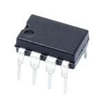
| 描述 | IC OPAMP GP 12MHZ 8DIP运算放大器 - 运放 Wide-Bandwidth Difet Op Amp |
| 产品分类 | Linear - Amplifiers - Instrumentation, OP Amps, Buffer Amps集成电路 - IC |
| 品牌 | Texas Instruments |
| 产品手册 | |
| 产品图片 |
|
| rohs | 符合RoHS无铅 / 符合限制有害物质指令(RoHS)规范要求 |
| 产品系列 | 放大器 IC,运算放大器 - 运放,Texas Instruments OPA606KPDifet® |
| 数据手册 | |
| 产品型号 | OPA606KP |
| 产品目录页面 | |
| 产品种类 | 运算放大器 - 运放 |
| 供应商器件封装 | 8-PDIP |
| 共模抑制比—最小值 | 78 dB |
| 关闭 | No Shutdown |
| 包装 | 管件 |
| 单位重量 | 523.200 mg |
| 压摆率 | 30 V/µs |
| 双重电源电压 | +/- 15 V |
| 商标 | Texas Instruments |
| 增益带宽生成 | 12 MHz |
| 增益带宽积 | 12MHz |
| 安装类型 | 通孔 |
| 安装风格 | Through Hole |
| 封装 | Tube |
| 封装/外壳 | 8-DIP(0.300",7.62mm) |
| 封装/箱体 | PDIP-8 |
| 工作温度 | 0°C ~ 70°C |
| 工作电源电压 | +/- 5 V to +/- 18 V |
| 工厂包装数量 | 50 |
| 技术 | BiFET |
| 放大器类型 | Wideband Amplifier |
| 最大双重电源电压 | +/- 18 V |
| 最大工作温度 | + 70 C |
| 最小双重电源电压 | +/- 5 V |
| 最小工作温度 | 0 C |
| 标准包装 | 50 |
| 电压-电源,单/双 (±) | 10 V ~ 36 V, ±5 V ~ 18 V |
| 电压-输入失调 | 300µV |
| 电流-电源 | 6.5mA |
| 电流-输入偏置 | 8pA |
| 电流-输出/通道 | 10mA |
| 电源电流 | 10 mA |
| 电路数 | 1 |
| 系列 | OPA606 |
| 转换速度 | 30 V/us |
| 输入偏压电流—最大 | 25 pA |
| 输入参考电压噪声 | 37 nV |
| 输入补偿电压 | 3 mV |
| 输出电流 | 10 mA |
| 输出类型 | - |
| 通道数量 | 1 Channel |


- 商务部:美国ITC正式对集成电路等产品启动337调查
- 曝三星4nm工艺存在良率问题 高通将骁龙8 Gen1或转产台积电
- 太阳诱电将投资9.5亿元在常州建新厂生产MLCC 预计2023年完工
- 英特尔发布欧洲新工厂建设计划 深化IDM 2.0 战略
- 台积电先进制程称霸业界 有大客户加持明年业绩稳了
- 达到5530亿美元!SIA预计今年全球半导体销售额将创下新高
- 英特尔拟将自动驾驶子公司Mobileye上市 估值或超500亿美元
- 三星加码芯片和SET,合并消费电子和移动部门,撤换高东真等 CEO
- 三星电子宣布重大人事变动 还合并消费电子和移动部门
- 海关总署:前11个月进口集成电路产品价值2.52万亿元 增长14.8%


PDF Datasheet 数据手册内容提取
® OPA606 Wide-Bandwidth Difet ® OPERATIONAL AMPLIFIER FEATURES APPLICATIONS l WIDE BANDWIDTH: 13MHz typ l OPTOELECTRONICS l HIGH SLEW RATE: 35V/m s typ l DATA ACQUISITION l LOW BIAS CURRENT: 10pA max at l TEST EQUIPMENT TA = +25(cid:176) C l AUDIO AMPLIFIERS l LOW OFFSET VOLTAGE: 500m V max l LOW DISTORTION: 0.0035% typ at 10kHz DESCRIPTION The OPA606 is a wide-bandwidth monolithic Laser-trimmed thin-film resistors offer improved off- dielectrically-isolated FET (Difet®) operational ampli- set voltage and noise performance. fier featuring a wider bandwidth and lower bias cur- The OPA606 is internally compensated for unity-gain rent than BIFET® LF156A amplifiers. Bias current is stability. specified under warmed-up and operating conditions, as opposed to a junction temperature of +25(cid:176) C. 1 5 7 Trim Trim +V CC 2 –In 3 +In V 6 OUT –V Simplified Circuit 4 CC Difet®; Burr-Brown Corp. BIFET®; National Semiconductor Corp. International Airport Industrial Park • Mailing Address: PO Box 11400 • Tucson, AZ 85734 • Street Address: 6730 S. Tucson Blvd. • Tucson, AZ 85706 Tel: (520) 746-1111 • Twx: 910-952-1111 • Cable: BBRCORP • Telex: 066-6491 • FAX: (520) 889-1510 • Immediate Product Info: (800) 548-6132 ©1985 Burr-Brown Corporation PDS-598D Printed in U.S.A. July, 1995 SBOS143
SPECIFICATIONS ELECTRICAL At V = – 15VDC and T = +25(cid:176)C unless otherwise noted. CC A OPA606KM OPA606LM OPA606KP PARAMETER CONDITIONS MIN TYP MAX MIN TYP MAX MIN TYP MAX UNITS FREQUENCY RESPONSE Gain Bandwidth Small Signal 10 12.5 11 13 9 12 MHz Full Power Response 20Vp-p, R = 2kW 515 550 470 kHz L Slew Rate V = – 10V, 22 33 25 35 20 30 V/m s O R = 2kW L Settling Time(1): 0.1% Gain = –1, 1.0 1.0 1.0 m s R = 2kW L 0.01% 10V Step 2.1 2.1 2.1 m s Total Harmonic Distortion G = +1, 20Vp-p 0.0035 0.0035 0.0035 % R = 2kW L f = 10kHz INPUT OFFSET VOLTAGE(2) Input Offset Voltage V = 0VDC – 180 – 1.5mV – 100 – 500 – 300 – 3mV m V CM Average Drift TA = TMIN to TMAX – 5 – 3 – 5 – 10 m V/(cid:176)C Supply Rejection V = – 10V to – 18V 82 100 90 104 80 90 dB CC – 10 – 79 – 6 – 32 – 32 – 100 m V/V BIAS CURRENT(2) Input Bias Current VCM = 0VDC – 7 – 15 – 5 – 10 – 8 – 25 pA OFFSET CURRENT(2) Input Offset Current V = 0VDC – 0.6 – 10 – 0.4 – 5 – 1 – 15 pA CM NOISE Voltage, f = 10Hz 100% tested (L) 37 30 40 37 nV/(cid:214) Hz O 100Hz 100% tested (L) 21 20 28 21 nV/(cid:214) Hz 1kHz 100% tested (L) 14 13 16 14 nV/(cid:214) Hz 10kHz (3) 12 11 13 12 nV/(cid:214) Hz 20kHz (3) 11 10.5 13 11 nV/(cid:214) Hz fB = 10Hz to 10kHz (3) 1.3 1.2 1.5 1.3 m Vrms Current, f = 0.1Hz thru 20kHz (3) 1.5 1.3 2 1.7 fA/(cid:214) Hz O IMPEDANCE Differential 1013 || 1 1013 || 1 1013 || 1 W || pF Common-Mode 1014 || 3 1014 || 3 1014 || 3 W || pF VOLTAGE RANGE Common-Mode Input Range – 10.5 – 11.5 – 11 – 11.6 – 10.2 – 11 V Common-Mode Rejection V = – 10VDC 80 95 85 96 78 90 dB IN OPEN-LOOP GAIN, DC Open-Loop Voltage Gain RL ‡ 2kW 95 115 100 118 90 110 dB RATED OUTPUT Voltage Output R = 2kW – 11 – 12.2 – 12 – 12.6 – 11 – 12 V L Current Output V = – 10VDC – 5 – 10 – 5 – 10 – 5 – 10 mA O Output Resistance DC, Open Loop 40 40 40 W Load Capacitance Stability Gain = +1 1000 1000 1000 pF Short Circuit Current 10 20 10 20 10 20 mA POWER SUPPLY Rated Voltage – 15 – 15 – 15 VDC Voltage Range, Derated Performance – 5 – 18 – 5 – 18 – 5 – 18 VDC Current, Quiescent I = 0mADC 6.5 9.5 6.2 9 6.5 10 mA O TEMPERATURE RANGE Specification Ambient Temperature KM, KP, LM 0 +70 0 +70 0 +70 (cid:176)C Operating Ambient Temperature –55 +125 –55 +125 –40 +85 (cid:176)C q 200 200 155 (cid:176)C/W JA NOTES: (1) See settling time test circuit in Figure 2. (2) Offset voltage, offset current, and bias current are measured with the units fully warmed up. (3) Sample tested–this parameter is guaranteed on L grade only. ® OPA606 2
ELECTRICAL (FULL TEMPERATURE RANGE SPECIFICATIONS) At V = – 15VDC and T = T to T unless otherwise noted. CC A MIN MAX OPA606KM OPA606LM OPA606KP PARAMETER CONDITIONS MIN TYP MAX MIN TYP MAX MIN TYP MAX UNITS TEMPERATURE RANGE Specification Range Ambient Temp. 0 +70 0 +70 0 +70 (cid:176)C INPUT OFFSET VOLTAGE(1) Input Offset Voltage V = 0VDC – 400 – 2mV – 335 – 750 – 750 – 3.5mV m V CM Average Drift – 5 – 3 – 5 – 10 m V/(cid:176)C Supply Rejection V = – 10V to – 18V 80 98 85 100 78 95 dB CC – 13 – 100 – 10 – 56 – 18 – 126 m V/V BIAS CURRENT(1) Input Bias Current V = 0VDC – 158 – 339 – 113 – 226 – 181 – 566 pA CM OFFSET CURRENT(1) Input Offset Current V = 0VDC – 14 – 226 – 9 – 113 – 23 – 339 pA CM VOLTAGE RANGE Common-Mode Input Range – 10.4 – 11.4 – 10.9 – 11.5 – 10 – 10.9 V Common-Mode Rejection VIN = – 10VDC 78 92 82 95 75 88 dB OPEN-LOOP GAIN, DC Open-Loop Voltage Gain R ‡ 2kW 90 106 95 112 88 104 dB L RATED OUTPUT Voltage Output R = 2kW – 10.5 – 12 – 11.5 – 12.4 – 10.4 – 11.8 V L Current Output VO = – 10VDC – 5 – 10 – 5 – 10 – 5 – 10 mA POWER SUPPLY Current, Quiescent IO = 0mADC 6.6 10 6.4 9.5 6.6 10.5 mA NOTES: (1) Offset voltage, offset current, and bias current are measured with the units fully warmed up. ABSOLUTE MAXIMUM RATINGS CONNECTION DIAGRAMS Supply Voltage..............................................................................– 18VDC Top View TO-99 Internal Power Dissipation (1).........................................................500mW NC Differential Input Voltage...............................................................– 36VDC Input Voltage Range.....................................................................– 18VDC 8 Storage Temperature Range...................................MP = = – 6–540(cid:176)C(cid:176)C to t o+ +15805(cid:176)(cid:176)CC Offset Trim 1 7 +VCC Operating Temperature Range................................M = –55(cid:176)C to +125(cid:176)C P = –40(cid:176)C to +85(cid:176)C Lead Temperature (soldering, 10s)................................................+300(cid:176)C –In 2 6 Output Output Short-Circuit Duration(3)................................................Continuous Junction Temperature....................................................................+175(cid:176)C 3 5 NOTES: (1) Packages must be derated based on q = 15(cid:176)C/W or q . (2) +In Offset Trim For supply voltages less than – 18VDC, the absJoClute maximum JAinput 4 voltage is equal to the negative supply voltage. (3) Short circuit may be to –VCC power supply common only. Rating applies to +25(cid:176)C ambient. Observe Case is connected to V dissipation limit and T. CC. J PACKAGE INFORMATION Top View DIP PACKAGE DRAWING MODEL PACKAGE NUMBER(1) Offset Trim(cid:13) 1(cid:13) 8(cid:13) NC(cid:13) OPA606KM TO-99 001 –In(cid:13) 2(cid:13) 7(cid:13) +V (cid:13) CC OPA606LM TO-99 001 OPA606KP Plastic DIP 006 +In(cid:13) 3(cid:13) 6(cid:13) Output(cid:13) NOTE: (1) For detailed drawing and dimension table, please see end of data –V 4 5 Offset Trim sheet, or Appendix D of Burr-Brown IC Data Book. CC ORDERING INFORMATION TEMPERATURE MODEL PACKAGE RANGE OPA606KM TO-99 0(cid:176)C to 70(cid:176)C OPA606LM TO-99 0(cid:176)C to 70(cid:176)C OPA606KP Plastic DIP 0(cid:176)C to 70(cid:176)C ® 3 OPA606
DICE INFORMATION PAD FUNCTION 1 Offset Trim 2 –In 3 +In 4 –V S 5 Offset Trim 6 Output 7 +VS 8 NC NC No Connection Substrate Bias: No Connection. MECHANICAL INFORMATION MILS (0.001") MILLIMETERS Die Size 65 x 54 – 5 1.65 x 1.37 – 0.13 Die Thickness 20 – 3 0.51 – 0.08 Min. Pad Size 4 x 4 0.10 x 0.10 Backing None OPA606 DIE TOPOGRAPHY Transistor Count 43 The information provided herein is believed to be reliable; however, BURR-BROWN assumes no responsibility for inaccuracies or omissions. BURR-BROWN assumes no responsibility for the use of this information, and all use of such information shall be entirely at the user’s own risk. Prices and specifications are subject to change without notice. No patent rights or licenses to any of the circuits described herein are implied or granted to any third party. BURR-BROWN does not authorize or warrant any BURR-BROWN product for use in life support devices and/or systems. ® OPA606 4
TYPICAL PERFORMANCE CURVES T = +25(cid:176)C, V = – 15VDC unless otherwise noted. A CC OPEN-LOOP FREQUENCY RESPONSE INPUT VOLTAGE NOISE SPECTRAL DENSITY 140(cid:13) 1k(cid:13) LM 120(cid:13) –45(cid:13) Voltage Gain (dB) 108640000(cid:13)(cid:13)(cid:13)(cid:13) Gain q ––9103(cid:13)5(cid:13) Phase Shift (degrees) (cid:214)oltage Noise (nV/ Hz) 10100(cid:13)(cid:13) V 20(cid:13) 0 –180 1 10 100 1k 10k 100k 1M 10M 100M 10 100 1k 10k 100k Frequency (Hz) Frequency (Hz) BIAS AND OFFSET CURRENT vs(cid:13) BIAS AND OFFSET CURRENT vs TEMPERATURE INPUT COMMON-MODE VOLTAGE 10nA(cid:13) 10nA(cid:13) 1nA(cid:13) 1nA(cid:13) 1nA(cid:13) 1nA(cid:13) Bias Current (pA) 10100(cid:13)(cid:13) IB IOS 11000(cid:13) (cid:13) Offset Current (pA) Bias Current (pA) 10100(cid:13)(cid:13) I B I OS 11000(cid:13) (cid:13) Offset Current (pA) 1(cid:13) 1(cid:13) 0.1 0.1 1 1 –50 –25 0 25 50 75 100 125 –15 –10 –5 0 5 10 15 Ambient Temperature (°C) Common-Mode Voltage (V) POWER SUPPLY REJECTION(cid:13) COMMON-MODE REJECTION(cid:13) vs FREQUENCY vs FREQUENCY 140(cid:13) 140(cid:13) ply Rejection (dB) 1120860000(cid:13)(cid:13)(cid:13)(cid:13) –VCC +VCC ode Rejection (dB) 1120860000(cid:13)(cid:13)(cid:13)(cid:13) p M Su n- er 40(cid:13) mo 40(cid:13) w m Po 20(cid:13) Co 20(cid:13) 0 0 10 100 1k 10k 100k 1M 10M 100M 10 100 1k 10k 100k 1M 10M 100M Frequency (Hz) Frequency (Hz) ® 5 OPA606
TYPICAL PERFORMANCE CURVES (CONT) T = +25(cid:176)C, V = – 15V unless otherwise noted. A CC MAXIMUM UNDISTORTED OUTPUT(cid:13) GAIN-BANDWIDTH AND SLEW RATE(cid:13) VOLTAGE vs FREQUENCY vs SUPPLY VOLTAGE 30(cid:13) 14(cid:13) 40(cid:13) GBW utput Voltage (V p-p) 2100(cid:13)(cid:13) ain-Bandwidth (MHz) 1120(cid:13)(cid:13) S/R 3350(cid:13)(cid:13) Slew Rate (V/µs) O G 0 8 25 10k 100k 1M 10M 0 5 10 15 20 Frequency (Hz) Supply Voltage (±VCC) SUPPLY CURRENT vs TEMPERATURE OPEN-LOOP GAIN vs TEMPERATURE 8(cid:13) 130(cid:13) mA) 7(cid:13) B) 120(cid:13) nt ( n (d Curre 6(cid:13) e Gai 110(cid:13) pply oltag u V S 5(cid:13) 100(cid:13) 4 90 –75 –50 –25 0 25 50 75 100 125 –75 –50 –25 0 25 50 75 100 125 Ambient Temperature (°C) Ambient Temperature (°C) GAIN-BANDWIDTH AND SLEW RATE(cid:13) OPEN-LOOP GAIN AND SUPPLY CURRENT(cid:13) vs TEMPERATURE vs SUPPLY VOLTAGE 16(cid:13) 38(cid:13) 10(cid:13) GBW 120(cid:13) 9(cid:13) Gain-Bandwidth (MHz) 111420(cid:13)(cid:13)(cid:13) S/R 333642(cid:13)(cid:13)(cid:13) Slew Rate (V/µs) Voltage Gain (dB) 110(cid:13) 876(cid:13)(cid:13)(cid:13) Supply Current (mA) 100 5(cid:13) 8 30 4 –75 –50 –25 0 25 50 75 100 125 0 5 10 15 20 Ambient Temperature (°C) Supply Voltage (±VCC) ® OPA606 6
TYPICAL PERFORMANCE CURVES (CONT) T = +25(cid:176)C, V = – 15V unless otherwise noted. A CC TOTAL HARMONIC DISTORTION(cid:13) SETTLING TIME vs CLOSED-LOOP GAIN vs FREQUENCY 10(cid:13) 0.01(cid:13) G = +1(cid:13) V = 7V %) O rms 8(cid:13) n ( 0.008(cid:13) e (µs) 6(cid:13) stortio 0.006(cid:13) m Di Ti c g ni Settlin 4(cid:13) Harmo 0.004(cid:13) 2(cid:13) Total 0.002(cid:13) Test Equipment(cid:13) Limit 0 0 1 10 100 1k 100 1k 10k 100k Closed-Loop Gain (V/V) Frequency (Hz) SMALL SIGNAL TRANSIENT RESPONSE(cid:13) LARGE SIGNAL TRANSIENT RESPONSE(cid:13) +80 +15 e (mV)(cid:13) +40 ge (V)(cid:13) g a olta 0 Volt 0 ut V put utp Out O +40 –80 –15 0 0.5 1 0 2.5 5 Time (µs)(cid:13) Time (µs)(cid:13) APPLICATIONS INFORMATION +V CC OFFSET VOLTAGE ADJUSTMENT (1) NOTE: (1) 10kW to 1MW (cid:13) The OPA606 offset voltage is laser-trimmed and will require Trim Potentiometer(cid:13) no further trim for most applications. As with most amplifi- 7 100kW (100kW Recommended) 1 ers, externally trimming the remaining offset can change 2 5 drift performance by about 0.5m V/(cid:176) C for each millivolt of 6 OPA606 adjusted offset. Note that the trim (Figure 1) is similar to 3 operational amplifiers such as LF156 and OP-16. The 4 ±50mV Typical(cid:13) Trim Range OPA606 can replace most other amplifiers by leaving the –V external null circuit unconnected. CC FIGURE 1. Offset Voltage Trim. ® 7 OPA606
INPUT PROTECTION Noninverting Buffer Static damage can cause subtle changes in amplifier input characteristics without necessarily destroying the device. In precision operational amplifiers (both bipolar and FET types), 2 2 6 6 this may cause a noticeable degradation of offset voltage and OPA606 OPA606 Out drift. Static protection is recommended when handling any In 3 Out 3 In precision IC operational amplifier. Inverting TO-99 Bottom View If the input voltage exceeds the amplifier’s negative supply In voltage, input current limiting must be used to prevent damage. 2 3 4 5 6 OPA606 6 7 3 Out 2 CIRCUIT LAYOUT 1 8 Wideband amplifiers require good circuit layout techniques and adequate power supply bypassing. Short, direct connec- tions and good high frequency bypass capacitors (ceramic or Mini-DIP Bottom View tantalum) will help avoid noise pickup or oscillation. BOARD LAYOUT(cid:13) 8 1 FOR INPUT GUARDING(cid:13) GUARDING AND SHIELDING Guard top and bottom of board.(cid:13) 7 2 As in any situation where high impedances are involved, Alternate: use Teflon® standoff(cid:13) careful shielding is required to reduce “hum” pickup in input for sensitive input pins. 6 3 Teflon® E. I. Du Pont(cid:13) leads. If large feedback resistors are used, they should also de Nemours & Co. 5 4 be shielded along with the external input circuitry. Leakage currents across printed circuit boards can easily FIGURE 3. Connection of Input Guard. exceed the bias current of the OPA606. To avoid leakage problems, it is recommended that the signal input lead of the APPLICATIONS CIRCUITS OPA606 be wired to a Teflon® standoff. If the OPA606 is to be soldered directly into a printed circuit board, utmost care 10kW must be used in planning the board layout. A “guard” pattern should completely surround the high +15VDC 0.1µF impedance input leads and should be connected to a low 1kW impedance point which is at the signal input potential (see Input 2 7 6 Figure 3). OPA606 Output BANDWIDTH > 1MHz(cid:13) 3 0.1µF T » 1.8µsec (0.01%)(cid:13) 4 S GAIN = –10V/V 0.1% –15VDC 2kW +15V FIGURE 4. Inverting Amplifier. +5V 0.1% –5V 2 7 6 2kW DUT 2N4416 3 0.1% 4 5kW 100pF +15VDC 3kW VOUT 0.1µF –15V Summing(cid:13) 0.1% G = –1 Node 2 7 6 Scope 5kW 3 OPA606 Output 2N4416 +15V Input 4 0.1µF Bandwidth > 12MHz(cid:13) 2kW Gain = +1V/V(cid:13) R » 1013W –15VDC IN FIGURE 5. Noninverting Buffer. FIGURE 2. Settling Time Test Circuit. ® OPA606 8
1MW 10kW C(cid:13) +15V 1 20pF CIunrpreuntt(cid:13) 2 7 VOoulttapguet(cid:13) 2 6 R1 Load 6 OPA606 i 3 OPA606 EO Input 3 100W 4 E = |i| R = 1V/µA O Optimize response for particular (cid:13) load condition with C and R. 1MW 1 1 i –15V FIGURE 8. Isolating Load Capacitance from Buffer. 0 0 3 Differential Gain = 1 + (2 x 10kW )/RG 6 FIGURE 6. Absolute Value Current-to-Voltage Circuit. OPA606 2 10kW » 0.2pF if necessary to(cid:13) R (cid:13) prevent gain peaking Differential(cid:13) 2kGW Differential(cid:13) Input Output 150kW 150kW 150kW 10kW 3 Metal-film(cid:13) 2 resistors 6 +15V OPA606 3 0.01µF 1. Bandwidth » 1.2MHz(cid:13) 2. Differential Gain = 11(cid:13) 2 7 3. Differential Output » 50Vp-p(cid:13) Pin Photodiode(cid:13) 6 4. Differential Slew Rate » 65V/µs OPA606 Output Motorola(cid:13) 3 MRD721 0.01µF FIGURE 9. Differential Input/Differential Output Amplifier. 4 0.1µF –15V 1. Circuit must be well shielded.(cid:13) 10kW 2. Stray capacitance is critical.(cid:13) 3. Bandwidth » 1MHz(cid:13) 4. Output » 22V/mW/cm2 +15V FIGURE 7. High-Speed Photodetector. 49.9W 2.49kW Total Mid-band Gain = 40dB(cid:13) (cid:13) See: "Topology Considerations for RIAA Phono Preamplifiers".(cid:13) AES reprint #1719.(cid:13) 2 October 1980, by Walter G. Jung Moving Magnet(cid:13) 6 Cartridge 3 OPA37EJ G » 51V/V 7.32kW G » 20V/V 47.5kW 150pF (1) 3 10µF 6 Output OPA606 0.1µF 2 1.05kW 3.74kW 10kW 1. Load R and C per cartridge manufacturer's recommendations.(cid:13) 0.3µF 200W 2. Use metal film resistors and plastic film capacitors.(cid:13) 3. Bypass ±V adequately. CC FIGURE 10. Low Noise/Low Distortion RIAA Preamplifier. ® 9 OPA606
IMPORTANT NOTICE Texas Instruments and its subsidiaries (TI) reserve the right to make changes to their products or to discontinue any product or service without notice, and advise customers to obtain the latest version of relevant information to verify, before placing orders, that information being relied on is current and complete. All products are sold subject to the terms and conditions of sale supplied at the time of order acknowledgment, including those pertaining to warranty, patent infringement, and limitation of liability. TI warrants performance of its semiconductor products to the specifications applicable at the time of sale in accordance with TI’s standard warranty. Testing and other quality control techniques are utilized to the extent TI deems necessary to support this warranty. Specific testing of all parameters of each device is not necessarily performed, except those mandated by government requirements. Customers are responsible for their applications using TI components. In order to minimize risks associated with the customer’s applications, adequate design and operating safeguards must be provided by the customer to minimize inherent or procedural hazards. TI assumes no liability for applications assistance or customer product design. TI does not warrant or represent that any license, either express or implied, is granted under any patent right, copyright, mask work right, or other intellectual property right of TI covering or relating to any combination, machine, or process in which such semiconductor products or services might be or are used. TI’s publication of information regarding any third party’s products or services does not constitute TI’s approval, warranty or endorsement thereof. Copyright 2000, Texas Instruments Incorporated