ICGOO在线商城 > 集成电路(IC) > 线性 - 放大器 - 仪表,运算放大器,缓冲器放大器 > AD8222ACPZ-R7
 Datasheet下载
- 型号: AD8222ACPZ-R7
- 制造商: Analog
- 库位|库存: xxxx|xxxx
- 要求:
| 数量阶梯 | 香港交货 | 国内含税 |
| +xxxx | $xxxx | ¥xxxx |
查看当月历史价格
查看今年历史价格
AD8222ACPZ-R7产品简介:
ICGOO电子元器件商城为您提供AD8222ACPZ-R7由Analog设计生产,在icgoo商城现货销售,并且可以通过原厂、代理商等渠道进行代购。 AD8222ACPZ-R7价格参考。AnalogAD8222ACPZ-R7封装/规格:线性 - 放大器 - 仪表,运算放大器,缓冲器放大器, Instrumentation Amplifier 2 Circuit 16-LFCSP-VQ (4x4)。您可以下载AD8222ACPZ-R7参考资料、Datasheet数据手册功能说明书,资料中有AD8222ACPZ-R7 详细功能的应用电路图电压和使用方法及教程。
AD8222ACPZ-R7是Analog Devices Inc.生产的一款高性能仪表放大器,广泛应用于对信号精度和稳定性要求较高的场合。其主要应用场景包括工业自动化、精密数据采集系统、传感器信号调理、医疗设备(如心电图机、血压监测仪等)、测试与测量仪器以及桥式传感器(如压力、应变片)的信号放大。

该器件具有低失调电压、低温漂、高共模抑制比(CMRR)和宽电源电压范围等特点,能够在恶劣电磁环境下准确提取微弱差分信号,有效抑制噪声和干扰。此外,AD8222ACPZ-R7采用紧凑的8引脚LFCSP封装,适合空间受限的高密度电路设计,并支持单电源或双电源供电,灵活性强。

在需要高精度模拟信号放大的系统中,AD8222ACPZ-R7可作为前端放大单元,提升整体系统的测量精度与可靠性,适用于工业过程控制、自动化检测设备及便携式仪器等关键领域。
| 参数 | 数值 |
| -3db带宽 | 1.2MHz |
| 产品目录 | 集成电路 (IC) |
| 描述 | IC OPAMP INSTR 1.2MHZ 16LFCSP |
| 产品分类 | Linear - Amplifiers - Instrumentation, OP Amps, Buffer Amps |
| 品牌 | Analog Devices Inc |
| 数据手册 | |
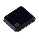
| 产品图片 |
|
| 产品型号 | AD8222ACPZ-R7 |
| PCN组件/产地 | |
| rohs | 无铅 / 符合限制有害物质指令(RoHS)规范要求 |
| 产品系列 | - |
| 产品培训模块 | http://www.digikey.cn/PTM/IndividualPTM.page?site=cn&lang=zhs&ptm=25193http://www.digikey.cn/PTM/IndividualPTM.page?site=cn&lang=zhs&ptm=30008http://www.digikey.cn/PTM/IndividualPTM.page?site=cn&lang=zhs&ptm=26202 |
| 产品目录页面 | |
| 供应商器件封装 | 16-LFCSP-VQ (4x4) |
| 其它名称 | AD8222ACPZ-R7DKR |
| 包装 | Digi-Reel® |
| 压摆率 | 2 V/µs |
| 增益带宽积 | - |
| 安装类型 | 表面贴装 |
| 封装/外壳 | 16-VQFN 裸露焊盘,CSP |
| 工作温度 | -40°C ~ 85°C |
| 放大器类型 | 仪表 |
| 标准包装 | 1 |
| 电压-电源,单/双 (±) | 4.6 V ~ 36 V, ±2.3 V ~ 18 V |
| 电压-输入失调 | 120µV |
| 电流-电源 | 900µA |
| 电流-输入偏置 | 500pA |
| 电流-输出/通道 | 18mA |
| 电路数 | 2 |
| 视频文件 | http://www.digikey.cn/classic/video.aspx?PlayerID=1364138032001&width=640&height=505&videoID=2245193153001 |
| 输出类型 | - |


- 商务部:美国ITC正式对集成电路等产品启动337调查
- 曝三星4nm工艺存在良率问题 高通将骁龙8 Gen1或转产台积电
- 太阳诱电将投资9.5亿元在常州建新厂生产MLCC 预计2023年完工
- 英特尔发布欧洲新工厂建设计划 深化IDM 2.0 战略
- 台积电先进制程称霸业界 有大客户加持明年业绩稳了
- 达到5530亿美元!SIA预计今年全球半导体销售额将创下新高
- 英特尔拟将自动驾驶子公司Mobileye上市 估值或超500亿美元
- 三星加码芯片和SET,合并消费电子和移动部门,撤换高东真等 CEO
- 三星电子宣布重大人事变动 还合并消费电子和移动部门
- 海关总署:前11个月进口集成电路产品价值2.52万亿元 增长14.8%


PDF Datasheet 数据手册内容提取
Precision, Dual-Channel Instrumentation Amplifier Data Sheet AD8222 FEATURES FUNCTIONAL BLOCK DIAGRAM TGwaion c sheatn wniethls 1 in r essmisatlol r4 p merm a ×m 4p lmifimer L (FGC =S P1 to 10,000) +VS OUT1 OUT2 –VS 16 15 14 13 Low noise AD8222 8 nV/√Hz at 1 kHz –IN1 1 12 –IN2 0.25 µV p-p (0.1 Hz to 10 Hz) RG1 2 11 RG2 High accuracy dc performance (B grade) RG1 3 10 RG2 +IN1 4 9 +IN2 60 µV maximum input offset voltage 0.3 µV/°C maximum input offset drift 5 6 7 8 11.206 n dAB m maixniimmuumm iCnMpuRtR b (Gia s= c 1u0r0re) nt +VS REF1 REF2 –VS 05947-001 Figure 1. Excellent ac performance 140 kHz bandwidth (G = 100) 13 µs settling time to 0.001% Differential output option (single channel) Fully specified Adjustable common-mode output Supply range: ±2.3 V to ±18 V APPLICATIONS Multichannel data acquisition for ECG and medical instrumentation Industrial process controls AD8222 maintains a minimum CMRR of 80 dB to 4 kHz for all Wheatstone bridge sensors grades at G = 1. High CMRR over frequency allows the AD8222 Differential drives for to reject wideband interference and line harmonics, greatly High resolution input ADCs simplifying filter requirements. The AD8222 also has a typical Remote sensors CMRR drift over temperature of just 0.07 µV/V/°C at G = 1. GENERAL DESCRIPTION The AD8222 operates on both single and dual supplies and only The AD8222 is a dual-channel, high performance instrumentation requires 2.2 mA maximum supply current for both amplifiers. amplifier that requires only one external resistor per amplifier It is specified over the industrial temperature range of −40°C to to set gains of 1 to 10,000. +85°C and is fully RoHS compliant. For a single-channel version, see the AD8221. The AD8222 is the first dual-instrumentation amplifier in the Table 1. Instrumentation Amplifiers by Category1 small 4 mm × 4mm LFCSP. It requires the same board area as a typical single instrumentation amplifier. The smaller package General- Military Low High Purpose Zero Drift Grade Power Speed PGA allows a 2× increase in channel density and a lower cost per AD8220 AD8231 AD620 AD8235 AD8250 channel, all with no compromise in performance. AD8221 AD8290 AD621 AD8236 AD8251 The AD8222 can also be configured as a single-channel, differen- AD8222 AD8293G80 AD524 AD627 AD8253 tial output instrumentation amplifier. Differential outputs provide AD8224 AD8553 AD526 AD623 high noise immunity, which can be useful when the output AD8228 AD8556 AD624 AD8223 signal must travel through a noisy environment, such as with AD8295 AD8557 AD8226 remote sensors. The configuration can also be used to drive AD8227 differential input analog-to-digital converters (ADCs). The 1 See www.analog.com for the latest selection of instrumentation amplifiers. Rev. B Document Feedback Information furnished by Analog Devices is believed to be accurate and reliable. However, no responsibility is assumed by Analog Devices for its use, nor for any infringements of patents or other One Technology Way, P.O. Box 9106, Norwood, MA 02062-9106, U.S.A. rights of third parties that may result from its use. Specifications subject to change without notice. No license is granted by implication or otherwise under any patent or patent rights of Analog Devices. Tel: 781.329.4700 ©2006–2016 Analog Devices, Inc. All rights reserved. Trademarks and registered trademarks are the property of their respective owners. Technical Support www.analog.com
AD8222 Data Sheet TABLE OF CONTENTS Features .............................................................................................. 1 Package Considerations ............................................................. 16 Applications ....................................................................................... 1 Layout .......................................................................................... 16 Functional Block Diagram .............................................................. 1 Input Bias Current Return Path ............................................... 17 General Description ......................................................................... 1 Input Protection ......................................................................... 18 Revision History ............................................................................... 2 RF Interference ........................................................................... 18 Specifications ..................................................................................... 3 Common-Mode Input Voltage Range ..................................... 18 Absolute Maximum Ratings ............................................................ 6 Applications Information .............................................................. 19 Thermal Resistance ...................................................................... 6 Differential Output .................................................................... 19 ESD Caution .................................................................................. 6 Driving a Differential Input ADC ............................................ 20 Pin Configuration and Function Descriptions ............................. 7 Precision Strain Gage ................................................................. 20 Typical Performance Characteristics ............................................. 8 Driving Cabling .......................................................................... 21 Theory of Operation ...................................................................... 15 Outline Dimensions ....................................................................... 22 Amplifier Architecture .............................................................. 15 Ordering Guide .......................................................................... 23 Gain Selection ............................................................................. 15 Reference Terminal .................................................................... 16 REVISION HISTORY 5/2016—Rev. A to Rev. B Changes to Thermal Resistance Section and Table 6 ................... 6 Changed CP-16-13 to CP-16-26 .................................. Throughout Changes to Figure 2 ........................................................................... 7 Change to Table 5 ............................................................................. 6 Changes to Figure 19 ...................................................................... 10 Changes to Figure 2 and Table 7 ..................................................... 7 Changes to Figure 43 ...................................................................... 14 Added Figure 3; Renumbered Sequentially .................................. 7 Changes to Reference Terminal Section, Figure 45, and Package Change to Input Protection Section ............................................. 18 Considerations Section .................................................................. 16 Updated Outline Dimensions ....................................................... 22 Deleted Thermal Pad Section ....................................................... 16 Changes to Ordering Guide .......................................................... 23 Added Package Without Thermal Pad and Package with Thermal Pad Sections .................................................................... 16 2/2010—Rev. 0 to Rev. A Changes to Figure 46 ...................................................................... 17 Added LFCSP_VQ, CP-16-13 Package ............................ Universal Deleted Solder Wash Section ........................................................ 17 Changes to Features Section and Table 1 ...................................... 1 Changes to RFI and Antialising Filter Section ........................... 20 Changed V to V , V to V , and T to T Throughout ..... 3 Updated Outline Dimensions ....................................................... 22 IN+ +IN IN− −IN A Change to Reference Input Parameter, Table 2 ............................. 4 Changes to Ordering Guide .......................................................... 23 Changed Output Short-Circuit Current to Output Short-Circuit Duration, Table 5 .............................................................................. 6 7/2006—Revision 0: Initial Version Rev. B | Page 2 of 24
Data Sheet AD8222 SPECIFICATIONS V = ±15 V, V = 0 V, T = 25°C, G = 1, R = 2 kΩ, unless otherwise noted. S REF A L Table 2. Single-Ended and Differential1 Output Configuration A Grade B Grade Parameter Test Conditions/Comments Min Typ Max Min Typ Max Unit COMMON-MODE REJECTION V = –10 V to +10 V CM RATIO (CMRR) CMRR DC to 60 Hz 1 kΩ source imbalance G = 1 80 86 dB G = 10 100 106 dB G = 100 120 126 dB G = 1000 130 140 dB CMRR at 4 kHz G = 1 80 80 dB G = 10 90 100 dB G = 100 100 110 dB G = 1000 100 110 dB CMRR Drift T = −40°C to +85°C, G = 1 0.07 0.07 µV/V/°C A NOISE Voltage Noise, 1 kHz RTI noise = √(e 2 + (e /G)2) NI NO Input Voltage Noise, e V , V , V = 0 V 8 8 nV/√Hz NI +IN −IN REF Output Voltage Noise, e V , V , V = 0 V 75 75 nV/√Hz NO +IN −IN REF RTI f = 0.1 Hz to 10 Hz G = 1 2 2 µV p-p G = 10 0.5 0.5 µV p-p G = 100 to 1000 0.25 0.25 µV p-p Current Noise f = 1 kHz 40 40 fA/√Hz f = 0.1 Hz to 10 Hz 6 6 pA p-p VOLTAGE OFFSET RTI V = (V ) + (V /G) OS OSI OSO Input Offset, V V = ±5 V to ±15 V 120 60 µV OSI S Over Temperature T = −40°C to +85°C 150 80 µV A Average TC 0.4 0.3 µV/°C Output Offset, V V = ±5 V to ±15 V 500 350 µV OSO S Over Temperature T = −40°C to +85°C 0.8 0.5 mV A Average TC 9 5 µV/°C Offset RTI vs. Supply (PSR) V = ±2.3 V to ±18 V S G = 1 90 110 94 110 dB G = 10 110 120 114 130 dB G = 100 124 130 130 140 dB G = 1000 130 140 140 150 dB INPUT CURRENT (PER CHANNEL) Input Bias Current, I 0.5 2.0 0.2 1.0 nA BIAS Over Temperature T = −40°C to +85°C 3.0 1.5 nA A Average TC 1 1 pA/°C Input Offset Current, I 0.2 1 0.1 0.5 nA OFFSET Over Temperature T = −40°C to +85°C 1.5 0.6 nA A Average TC 1 0.5 2 pA/°C Rev. B | Page 3 of 24
AD8222 Data Sheet A Grade B Grade Parameter Test Conditions/Comments Min Typ Max Min Typ Max Unit REFERENCE INPUT R 20 20 kΩ IN I V , V , V = 0 V 50 60 50 60 µA IN +IN −IN REF Voltage Range −V +V −V +V V S S S S Reference Gain to Output 1 1 V/V Reference Gain Error 0.01 0.01 % GAIN G = 1 + (49.4 kΩ/R ) G Gain Range 1 10,000 1 10,000 V/V Gain Error V ± 10 V OUT G = 1 0.05 0.02 % G = 10 0.3 0.15 % G = 100 0.3 0.15 % G = 1000 0.3 0.15 % Gain Nonlinearity V = –10 V to +10 V OUT G = 1 3 10 1 5 ppm G = 10 7 20 7 20 ppm G = 100 7 20 7 20 ppm Gain vs. Temperature G = 1 3 10 2 5 ppm/°C G > 12 −50 −50 ppm/°C INPUT Input Impedance Differential 100||2 100||2 GΩ||pF Common Mode 100||2 100||2 GΩ||pF Input Operating Voltage Range3 V = ±2.3 V to ±5 V −V + 1.9 +V − 1.1 −V + 1.9 +V − 1.1 V S S S S S Over Temperature T = −40°C to +85°C −V + 2.0 +V − 1.2 −V + 2.0 +V − 1.2 V A S S S S Input Operating Voltage Range3 V = ±5 V to ±18 V −V + 1.9 +V − 1.2 −V + 1.9 +V − 1.2 V S S S S S Over Temperature T = −40°C to +85°C −V + 2.0 +V − 1.2 −V + 2.0 +V − 1.2 V A S S S S OUTPUT R = 10 kΩ L Output Swing V = ±2.3 V to ±5 V −V + 1.1 +V − 1.2 −V + 1.1 +V − 1.2 V S S S S S Over Temperature T = −40°C to +85°C −V + 1.4 +V − 1.3 −V + 1.4 +V − 1.3 V A S S S S Output Swing V = ±5 V to ±18 V −V + 1.2 +V − 1.4 −V + 1.2 +V − 1.4 V S S S S S Over Temperature T = −40°C to +85°C −V + 1.6 +V − 1.5 −V + 1.6 +V − 1.5 V A S S S S Short-Circuit Current 18 18 mA POWER SUPPLY Operating Range V = ±2.3 V to ±18 V ±2.3 ±18 ±2.3 ±18 V S Quiescent Current (per Amplifier) 0.9 1.1 0.9 1.1 mA Over Temperature T = −40°C to +85°C 1 1.2 1 1.2 mA A TEMPERATURE RANGE Specified Performance −40 +85 −40 +85 °C Operational4 −40 +125 −40 +125 °C 1 Refers to differential configuration shown in Figure 50. 2 Does not include the effects of external resistor, RG. 3 One input grounded. G = 1. 4 See the Typical Performance Characteristics section for expected operation between 85°C and 125°C. Rev. B | Page 4 of 24
Data Sheet AD8222 V = ±15 V, V = 0 V, T = 25°C, R = 2 kΩ, unless otherwise noted. S REF A L Table 3. Single-Ended Output Configuration—Dynamic Performance (Both Amplifiers) A Grade B Grade Parameter Test Conditions/Comments Min Typ Max Min Typ Max Unit DYNAMIC RESPONSE Small Signal −3 dB Bandwidth G = 1 1200 1200 kHz G = 10 750 750 kHz G = 100 140 140 kHz G = 1000 15 15 kHz Settling Time 0.01% 10 V step G = 1 to 100 10 10 µs G = 1000 80 80 µs Settling Time 0.001% 10 V step G = 1 to 100 13 13 µs G = 1000 110 110 µs Slew Rate G = 1 1.5 2 1.5 2 V/µs G = 5 to 1000 2 2.5 2 2.5 V/µs Table 4. Differential Output Configuration1—Dynamic Performance A Grade B Grade Parameter Test Conditions/Comments Min Typ Max Min Typ Max Unit DYNAMIC RESPONSE Small Signal −3 dB Bandwidth G = 1 1000 1000 kHz G = 10 650 650 kHz G = 100 140 140 kHz G =1000 15 15 kHz Settling Time 0.01% 10 V step G = 1 to 100 15 15 µs G = 1000 80 80 µs Settling Time 0.001% 10 V step G = 1 to 100 18 18 µs G = 1000 110 110 µs Slew Rate G = 1 1.5 2 1.5 2 V/µs G = 5 to 1000 2 2.5 2 2.5 V/µs 1 Refers to differential configuration shown in Figure 50. Rev. B | Page 5 of 24
AD8222 Data Sheet ABSOLUTE MAXIMUM RATINGS THERMAL RESISTANCE Table 5. Parameter Rating Table 6. Supply Voltage ±18 V Package θ Unit JA Output Short-Circuit Current Duration Indefinite CP-16-19: LFCSP Without Thermal Pad 86 °C/W Input Voltage (Common Mode) ±V S CP-16-26: LFCSP with Thermal Pad 48 °C/W Differential Input Voltage ±V S The θ values in Table 6 assume a 4-layer JEDEC standard Storage Temperature Range −65°C to +130°C JA board. For the LFCSP with thermal pad, it is assumed that the Operational Temperature Range −40°C to +125°C thermal pad is soldered to a landing on the PCB board, with the Package Glass Transition Temperature (T ) 130°C G landing thermally connected to a heat dissipating power plane. ESD θ at the exposed pad is 4.4°C/W. Human Body Model 2 kV JC Charge Device Model 1 kV Maximum Power Dissipation Stresses at or above those listed under Absolute Maximum The maximum safe power dissipation for the AD8222 is limited Ratings may cause permanent damage to the product. This is a by the associated rise in junction temperature (T) on the die. At J stress rating only; functional operation of the product at these approximately 130C, which is the glass transition temperature, or any other conditions above those indicated in the operational the plastic changes its properties. Even temporarily exceeding section of this specification is not implied. Operation beyond this temperature limit may change the stresses that the package the maximum operating conditions for extended periods may exerts on the die, permanently shifting the parametric performance affect product reliability. of the amplifiers. Exceeding a temperature of 130°C for an extended period can result in a loss of functionality. ESD CAUTION Rev. B | Page 6 of 24
Data Sheet AD8222 PIN CONFIGURATIONS AND FUNCTION DESCRIPTIONS 12 1 2 +VSOUTOUT–VS +VS OUT OUT –VS 16 151413 61 51 41 31 –IN11 PIN1 12–IN2 INDICATOR –IN1 1 12 –IN2 RG12 11RG2 AD8222 RG1 2 AD8222 11 RG2 RG13 10RG2 TOP VIEW TOP VIEW +IN14 9 +IN2 RG1 3 (Not to Scale) 10 RG2 +IN1 4 9 +IN2 +V5SREF16REF27 –V8S 05947-002 5VS 6F1 7F2 8VS + E E – R R N1.O TTHEES EXPOSEDPAD MUST BE CONNECTEDTO –VS. 05947-102 Figure 2. 16-Lead LFCSP (CP-16-19) Pin Configuration Figure 3. 16-Lead LFCSP (CP-16-26) Pin Configuration Table 7. Pin Function Descriptions Pin No. CP-16-19 CP-16-26 Mnemonic Description 1 1 −IN1 Negative Input In-Amp 1. 2, 3 2, 3 RG1 Gain Resistor In-Amp 1. 4 4 +IN1 Positive Input In-Amp 1. 5, 16 5, 16 +V Positive Supply. S 6 6 REF1 Reference Adjust In-Amp 1. 7 7 REF2 Reference Adjust In-Amp 2. 8, 13 8, 13 −V Negative Supply. S 9 9 +IN2 Positive Input In-Amp 2. 10, 11 10, 11 RG2 Gain Resistor In-Amp 2. 12 12 −IN2 Negative Input In-Amp 2. 14 14 OUT2 Output In-Amp 2. 15 15 OUT1 Output In-Amp 1. Not applicable 0 EPAD Exposed Pad. The exposed pad must be connected to −V. S Rev. B | Page 7 of 24
AD8222 Data Sheet TYPICAL PERFORMANCE CHARACTERISTICS 500 N = 1713 800 400 TS TS 600 NI NI F U 300 F U O O R R E E 400 B B M 200 M U U N N 200 100 0 0 –50 –40 –30 –20 –1C0MRR0 (µV/V1)0 20 30 40 50 05947-003 –2.0 –1.5 –1.0 –0.5IOFFSE0T (nA)0.5 1.0 1.5 2.0 05947-006 Figure 4. Typical Distribution for CMRR (G = 1) Figure 7. Typical Distribution of Input Offset Current 15 N = 1713 300 250 GE (V) 10 VS = ±15V S N T A 5 UNI 200 E R OF OD ER 150 N-M 0 B O M M U M VS = ±5V N 100 O –5 C T U 10 NP –10 I 0 –100 80 60 40 20VOS0I (µV)20 40 60 80 100 05947-004 –15–15 –10 –O5UTPUT V0OLTAGE (V5) 10 15 05947-007 Figure 5. Typical Distribution of Input Offset Voltage Figure 8. Input Common-Mode Range vs. Output Voltage, G = 1 15 N = 1713 700 V) 10 600 E ( G VS = ±15V S N NIT 500 RA 5 U E ER OF 400 N-MOD 0 B O M 300 M NU OM –5 VS = ±5V 200 T C U P 100 IN –10 0 –2.0 –1.5 –1.0 –0.5 IBIAS0 (nA) 0.5 1.0 1.5 2.0 05947-005 –15–15 –10 –O5UTPUT V0OLTAGE (V5) 10 15 05947-008 Figure 6. Typical Distribution of Input Bias Current Figure 9. Input Common-Mode Range vs. Output Voltage, G = 100 Rev. B | Page 8 of 24
Data Sheet AD8222 200 160 150 150 140 BANDWIDTH T (pA) 100 VS = ±15V 111321000 GAIN = 100L0IMITED N 50 100 AS CURRE 0 VS = ±5V PSRR (dB) 987000 GAIN = 100 BI –50 + 60 UT 50 GAIN = 10 P N –100 40 I GAIN = 1 30 –150 20 10 –200 0 –15 –10 COM–M5ON-MOD0E VOLTAG5E (V) 10 15 05947-009 0.1 1 10 FR1E0Q0UENCY1 k(Hz) 10k 100k 1M 05947-012 Figure 10. IBIAS vs. Common-Mode Voltage Figure 13. Positive PSRR vs. Frequency, RTI (G = 1 to 1000) 2.0 160 150 µV) 1.8 140 AGE ( 1.6 113200 GAIN = 1000 T OFFSET VOL 111...024 RR (dB) 1110980000 GAIN = 100 PUT 0.8 –PS 7600 N N I 0.6 50 GE I 0.4 4300 GAIN = 10 N CHA 0.2 2100 GAIN = 1 0 0 0 2 WARM4-UP TIME (M6inutes) 8 10 05947-010 0.1 1 10 FR1E0Q0UENCY1 k(Hz) 10k 100k 1M 05947-013 Figure 11. Change in Input Offset Voltage vs. Warm-Up Time Figure 14. Negative PSRR vs. Frequency, RTI (G = 1 to 1000) 1000 10k 800 NEGATIVE V) RENT (pA) 642000000 POSITIVE O 85°C RTI (µ 1k GAIN = 1 R T S CU 0 OFFSET CURRENT 25°C 100 GAIN = 10 GAIN = 100 NPUT BIA ––240000 L DRIFT: 10 I –600 TA GAIN = 1000 O T –800 –1000 1 –55 –35 –15 5TEMP2E5RATU4R5E (°C6)5 85 105 125 05947-011 1 10 10S0OURCE1k RESIST10AkNCE (1Ω0)0k 1M 10M 05947-014 Figure 12. Input Bias Current and Offset Current vs. Temperature Figure 15. Total Drift vs. Source Resistance Rev. B | Page 9 of 24
AD8222 Data Sheet 70 20 GAIN = 1000 60 15 50 GAIN = 100 10 40 AIN (dB) 123000 GAIN = 10 MR (µV/V) 50 EXAMPLE PART 1 G 0 GAIN = 1 ∆C –5 EXAMPLE PART 2 –10 –10 –20 –15 –30 –40 –20 100 1k F1R0EkQUENCY1 (0H0zk) 1M 10M 05947-015 –40 –20 0 T2E0MPER4A0TURE6 (0°C) 80 100 120 05947-018 Figure 16. Gain vs. Frequency Figure 19. ΔCMR vs. Temperature, G = 1 160 GAIN = 1000 +VS–0 150 –0.4 140 GAIN = 100 ES–0.8 FROM +VS G 113200 GAIN = 10 BANDWIDTH MIT (V)VOLTA––11..62 R (dB) 111000 GAIN = 1 LIMITED AGE LIUPPLY –2.0 CMR 90 VOLTTO S+2.0 FROM –VS 80 UT ED +1.6 PR 70 INER+1.2 F 60 RE+0.8 50 +0.4 400.1 1 10 FR1E0Q0UENCY1 k(Hz) 10k 100k 1M 05947-016 –VS+02 6 SUPPLY V1O0LTAGE (V) 14 18 05947-019 Figure 17. CMRR vs. Frequency, RTI Figure 20. Input Voltage Limit vs. Supply Voltage, G = 1 160 +VS–0 GAIN = 1000 150 –0.4 CMRR (dB) 11111432109000000 GGAAIINN == 11000 BALNIMDWITEIDDTH VOLTAGE SWING (V)TO SUPPLY VOLTAGES+–––1101....6286 RL = 10kΩ RL = 2kΩ 80 PUT RED +1.2 RL = 2kΩ 70 UTER GAIN = 1 OF+0.8 60 RE RL = 10kΩ +0.4 50 400.1 1 10 FR1E0Q0UENCY1 k(Hz) 10k 100k 1M 05947-017 –VS+02 6 SUPPLY V1O0LTAGE (V) 14 18 05947-020 Figure 18. CMRR vs. Frequency, RTI, 1 kΩ Source Imbalance Figure 21. Output Voltage Swing vs. Supply Voltage, G = 1 Rev. B | Page 10 of 24
Data Sheet AD8222 30 40 30 p) SWING (V p- 20 10ppm/DIV) 2100 2kΩ LOAD LTAGE ARITY ( 0 UT VO 10 NLINE –10 600Ω LOAD 10kΩ LOAD P O –20 T N U O –30 01 10 LOAD RES1I0S0TANCE (Ω) 1k 10k 05947-021 –40–10 –8 –6 –4 –2VOU0T (V) 2 4 6 8 10 05947-024 Figure 22. Output Voltage Swing vs. Load Resistance Figure 25. Gain Nonlinearity, G = 100 +VS–0 Hz) 1k –1 SOURCING V/ S n G (V)TAGE –2 SITY ( GAIN = 1 PUT VOLTAGE SWINRED TO SUPPLY VOL +–33 OISE SPECTRAL DEN10100 GGAAIINN == 11000 OUTEFER +2 SINKING GE N GAIN = 1000 R A +1 T OL GAIN = 1000 V BW LIMIT –VS+00 1 2 3 O4UTPU5T CU6RREN7T (m8A) 9 10 11 12 05947-022 11 10 F1R0E0QUENCY (1Hkz) 10k 100k 05947-026 Figure 23. Output Voltage Swing vs. Output Current, G = 1 Figure 26. Voltage Noise Spectral Density vs. Frequency (G = 1 to 1000) 4 3 V) 2 DI m/ p 1 p 10kΩ LOAD 1 Y ( T 0 RI A 2kΩ LOAD E N –1 LI 600Ω LOAD N NO –2 ––34 05947-027 –10 –8 –6 –4 –2VOU0T (V) 2 4 6 8 10 05947-023 2µV/DIV 1s/DIV Figure 24. Gain Nonlinearity, G = 1 Figure 27. 0.1 Hz to 10 Hz RTI Voltage Noise (G = 1) Rev. B | Page 11 of 24
AD8222 Data Sheet 30 GAIN = 10, 100, 1000 GAIN = 1 25 p) p- V E ( 20 G A T L O 15 V T U P UT 10 O X A M 5 05947-028 0 0.1µV/DIV 1s/DIV 1k 10kFREQUENCY (Hz1)00k 1M 05947-031 Figure 28. 0.1 Hz to 10 Hz RTI Voltage Noise (G = 1000) Figure 31. Large Signal Frequency Response 1k Hz) A/ Y (f 5V/DIV T SI N E D L A R T 100 C E P S 7.4µs TO 0.01% E 8.3µs TO 0.001% S OI N T 0.002%/DIV N E CURR 10 20µs/DIV 05947-032 1 10 F1R0E0QUENCY (1Hkz) 10k 100k 05947-029 Figure 29. Current Noise Spectral Density vs. Frequency Figure 32. Large Signal Pulse Response and Settling Time (G = 1) 5V/DIV 4.8µs TO 0.01% 6.6µs TO 0.001% 0.002%/DIV 05947-030 20µs/DIV 05947-033 5pA/DIV 1s/DIV Figure 30. 0.1 Hz to 10 Hz Current Noise Figure 33. Large Signal Pulse Response and Settling (G = 10) Rev. B | Page 12 of 24
Data Sheet AD8222 5V/DIV 9.2µs TO 0.01% 16.2µs TO 0.001% 0.002%/DIV 20µs/DIV 05947-034 20mV/DIV 4µs/DIV 05947-037 Figure 34. Large Signal Pulse Response and Settling Time (G = 100) Figure 37. Small Signal Response, G = 10, RL = 2 kΩ, CL = 100 pF 5V/DIV 83µs TO 0.01% 112µs TO 0.001% 0.002%/DIV 200µs/DIV 05947-035 20mV/DIV 10µs/DIV 05947-038 Figure 35. Large Signal Pulse Response and Settling Time (G = 1000) Figure 38. Small Signal Response, G = 100, RL = 2 kΩ, CL = 100 pF 20mV/DIV 4µs/DIV 05947-036 20mV/DIV 100µs/DIV 05947-039 Figure 36. Small Signal Response, G = 1, RL = 2 kΩ, CL = 100 pF Figure 39. Small Signal Response, G = 1000, RL = 2 kΩ, CL = 100 pF Rev. B | Page 13 of 24
AD8222 Data Sheet 15 60 GAIN = 1000 40 GAIN = 100 µs) 10 G TIME ( SETTLED TO 0.001% N (dB) 20 GAIN = 10 TTLIN SETTLED TO 0.01% GAI 0 GAIN = 1 E 5 S –20 0 –40 0 O5UTPUT VOLTA1G0E STEP SIZE (1V5) 20 05947-040 100 1k F1R0EkQUENCY1 (0H0zk) 1M 10M 05947-043 Figure 40. Settling Time vs. Step Size (G = 1) Figure 43. Differential Output Configuration: Gain vs. Frequency 1k 100 OUTPUT BALANCE = 20 logVDIFF_OUT 90 VCM_OUT 80 E (µs) 100 CE (dB) 7600 MELAISMSYIUTSRETEDEM MBEYNT M N G TI ALA 50 N B TLI SETTLED TO 0.001% UT 40 ET 10 TP S U 30 O SETTLED TO 0.01% 20 10 1 0 1 10 GAIN 100 1k 05947-041 1 10 100FREQUE1kNCY (Hz)10k 100k 1M 05947-056 Figure 41. Settling Time vs. Gain for a 10 V Step Figure 44. Differential Output Configuration: Output Balance vs. Frequency 200 SOURCE SOURCE VOUT VOUT = 20V p-p SMALLER TO 180 AVOID SLEW RATE LIMIT B) GAIN = 1000 N (d 160 O THERMAL CROSSTALK TI VARIES WITH LOAD A 140 R A P E S 120 L E GAIN = 1 N AN 100 H C 80 60 1 10 100FREQUE1kNCY (Hz)10k 100k 1M 05947-042 Figure 42. Channel Separation vs. Frequency, RL = 2 kΩ, Source Channel at G = 1 Rev. B | Page 14 of 24
Data Sheet AD8222 THEORY OF OPERATION I VB I IB COMPENSATION A1 A2 IB COMPENSATION 10kΩ C1 C2 +VS 10kΩ OUTPUT A3 10kΩ +VS +VS R1 24.7kΩ R2 24.7kΩ +VS –VS –IN 400Ω Q1 +VS +VS Q2 400Ω +IN 10kΩ REF RG –VS –VS –VS –VS –VS 05947-045 Figure 45. Simplified Schematic AMPLIFIER ARCHITECTURE GAIN SELECTION The two instrumentation amplifiers of the AD8222 are based Placing a resistor across the R terminals sets the gain of the G on the classic 3-op-amp topology. Figure 45 shows a simplified AD8222, which can be calculated by referring to Table 8 or by schematic of one of the amplifiers. The input transistors, Q1 using the following gain equation: and Q2, are biased at a fixed current. Any differential input 49.4kΩ signal forces the output voltages of A1 and A2 to change so that R G G1 the differential voltage also appears across R . The current that G flows through R must also flow through R1 and R2, resulting G Table 8. Gains Achieved Using 1% Resistors in a precisely amplified version of the differential input signal between the outputs of A1 and A2. Topologically, Q1 + A1 + R1 1% Standard Table Value of RG (Ω) Calculated Gain and Q2 + A2 + R2 can be viewed as precision current feedback 49.9 k 1.990 amplifiers. The common-mode signal and the amplified differen- 12.4 k 4.984 tial signal are applied to a difference amplifier that rejects the 5.49 k 9.998 common-mode voltage. The difference amplifier employs innova- 2.61 k 19.93 tions that result in low output offset voltage as well as low output 1.00 k 50.40 offset voltage drift. 499 100.0 249 199.4 Because the input amplifiers employ a current feedback architec- 100 495.0 ture, the gain-bandwidth product of the AD8222 increases 49.9 991.0 with gain, resulting in a system that does not suffer from the The AD8222 defaults to G = 1 when no gain resistor is used. expected bandwidth loss of voltage feedback architectures at The tolerance and gain drift of the R resistor should be added higher gains. G to the AD8222 specifications to determine the total gain The transfer function of the AD8222 is accuracy of the system. When the gain resistor is not used, gain error and gain drift are kept to a minimum. V = G(V − V ) + V OUT +IN −IN REF where: 49.4kΩ G1 RG Rev. B | Page 15 of 24
AD8222 Data Sheet REFERENCE TERMINAL in the Outline Dimensions section. This metal is connected to −V through the device. Because of a possibility of a short, vias S The output voltage of an AD8222 channel is developed with should not be placed underneath this exposed metal. respect to the potential on the corresponding reference terminal. Typically, the reference terminal is connected to ground, but it Package with Thermal Pad can also be driven with a voltage to offset the output signal. For This package is included primarily for legacy reasons. Because example, connect a voltage to the reference terminal to level- the AD8222 dissipates so little power, there is little need for the shift the output so that the AD8222 can drive a single-supply thermal pad. ADC. Both REF1 and REF2 are protected with ESD diodes and should not exceed either +VS or −VS by more than 0.3 V. The thermal pad is connected internally to −VS. The pad can either be left unsoldered, soldered to an otherwise unconnected For best performance, source impedance to a reference terminal PCB landing, or soldered to a landing connected to the negative should be kept below 1 Ω. As shown in Figure 45, the reference supply rail (−V). If pin compatibility with the AD8224 is S terminal is at one end of a 10 kΩ resistor. Additional impedance desired, the pad should not be electrically connected to any net, at the reference terminal adds to this 10 kΩ resistor and results including −V. S in amplification of the signal connected to the positive input. The amplification from the additional R can be computed by The solder process can leave flux and other contaminants on REF the board. When these contaminants are between the AD8222 2 10kΩR REF leads and thermal pad, they can create leakage paths that are 20kΩR REF larger than the bias currents of the AD8222. A thorough washing process removes these contaminants and restores the Only the positive signal path is amplified; the negative path is excellent bias current performance of the AD8222. unaffected. This uneven amplification degrades the CMRR of the amplifier. LAYOUT INCORRECT CORRECT CORRECT The AD8222 is a high precision device. To ensure optimum performance at the PC board level, take care in the design of the board layout. The AD8222 pinout is arranged in a logical AD8222 AD8222 AD8222 manner to aid in this task. REF REF REF V V Common-Mode Rejection Over Frequency V The AD8222 has a higher CMRR over frequency than typical + + in-amps, which gives it greater immunity to disturbances, such OP2177 AD8222 – – 05947-054 alasy loinuet inso riesqeu ainredd i ttso a mssaoicnitaatiend thhaisr mhiognhi cpse.r Afo wrmelal-nicme.p Ilenmpuetn ted Figure 46. Driving the Reference Pin source impedances should be matched closely. Source resistance should be placed close to the inputs so that it interacts with as PACKAGE CONSIDERATIONS little parasitic capacitance as possible. The AD8222 comes in a 4 mm × 4 mm LFCSP. Beware of Parasitics at the RGx pins can also affect CMRR over frequency. blindly copying the footprint from another 4 mm × 4 mm The PCB should be laid out so that the parasitic capacitances at LFCSP device; the landing pattern may be different. Refer to each pin match. Traces from the gain setting resistor to the RGx the Outline Dimensions section to verify that the PCB symbol pins should be kept short to minimize parasitic inductance. has the correct dimensions. Reference The AD8222 comes in two package varieties, both with and without a thermal pad. Errors introduced at the reference terminal feed directly to the output. Take care to tie REF to the appropriate local ground. Package Without Thermal Pad Power Supplies The AD8222 ships with a package that does not include a thermal pad; it is the preferred package for the AD8222. Unlike chip Use a stable dc voltage to power the instrumentation amplifier. scale packages where the pad limits routing capability, the AD8222 Noise on the supply pins can adversely affect performance. package allows routes and vias directly underneath the chip, so The AD8222 has two positive supply pins (Pin 5 and Pin 16) and that the full space savings of the small LFCSP can be realized. two negative supply pins (Pin 8 and Pin 13). Although the device Although the package has no metal in the center of the device, functions with only one pin from each supply pair connected, both the manufacturing process does leave a very small section of pins should be connected for specified performance and exposed metal at each of the package corners, shown in Figure 56 optimum reliability. Rev. B | Page 16 of 24
Data Sheet AD8222 The AD8222 should be decoupled with 0.1 μF bypass capacitors, INPUT BIAS CURRENT RETURN PATH one for each supply. The positive supply decoupling capacitor The input bias current of the AD8222 must have a return path should be placed near Pin 16, and the negative supply decoupl- to common. When the source, such as a thermocouple, cannot ing capacitor should be placed near Pin 8. Each supply should provide a return current path, one should be created, as shown also be decoupled with a 10 μF tantalum capacitor. The tantalum in Figure 48. capacitor can be placed further away from the AD8222 and can generally be shared by other precision integrated circuits. Figure 47 INCORRECT CORRECT shows an example layout. +VS +VS AD8222 AD8222 REF REF 0.1µF –VS –VS TRANSFORMER TRANSFORMER 16 15 14 13 AD8222 +VS +VS 1 12 2 11 RG1 RG2 AD8222 AD8222 3 10 REF REF 4 9 10MΩ 5 6 7 8 –VS –VS THERMOCOUPLE THERMOCOUPLE +VS +VS C C 0.1µF AD8222 fHIGH-PASS =2π1RC R AD8222 05947-046 C REF C R REF Figure 47. Example Layout CAPACITIVE–LVYS COUPLED CAPACITIVELY COUP–LVESD 05947-047 Figure 48. Creating an IBIAS Path Rev. B | Page 17 of 24
AD8222 Data Sheet INPUT PROTECTION +15V All terminals of the AD8222 are protected against ESD (2 kV, 0.1µF 10µF human body model). In addition, the input structure allows for dc overload conditions of about 2.5 V beyond the supplies. CC 1nF R +IN Input Voltages Beyond the Rails 4.02kΩ For larger input voltages, an external resistor should be used in CD R1 AD8222 VOUT 10nF 499Ω series with each input to limit current during overload conditions. R REF The AD8222 can safely handle a continuous 6 mA current. The 4.02kΩ –IN CC limiting resistor can be computed from 1nF V V 0.1µF 10µF RLIMIT IN6mSAUPPLY 400Ω –15V 05947-048 Figure 49. RFI Suppression For applications in which the AD8222 encounters extreme over- load voltages, such as cardiac defibrillators, external series Figure 49 shows an example where the differential filter fre- resistors and low leakage diode clamps, such as the BAV199L, quency is approximately 2 kHz, and the common-mode filter the FJH1100, or the SP720, should be used. frequency is approximately 40 kHz. Differential Input Voltages at High Gains Values of R and C should be chosen to minimize RFI. Mismatch C When operating at high gain, large differential input voltages between the R × CC at the positive input and the R × CC at can cause more than 6 mA of current to flow into the inputs. negative input degrades the CMRR of the AD8222. By using a This condition occurs when the differential voltage exceeds value of CD 10× larger than the value of CC, the effect of the the following critical voltage: mismatch is reduced and performance is improved. VCRITICAL = (400 + RG) × (6 mA) COMMON-MODE INPUT VOLTAGE RANGE This is true for differential voltages of either polarity. The 3-op-amp architecture of the AD8222 applies gain and then removes the common-mode voltage. Therefore, internal nodes The maximum allowed differential voltage can be increased by in the AD8222 experience a combination of both the gained adding an input protection resistor in series with each input. signal and the common-mode signal. This combined signal can The value of each protection resistor should be be limited by the voltage supplies even when the individual R = (V − V )/6 mA input and output signals are not. Figure 8 and Figure 9 show the PROTECT DIFF_MAX CRITICAL allowable common-mode input voltage ranges for various RF INTERFERENCE output voltages, supply voltages, and gains. RF rectification is often a problem when amplifiers are used in applications where there are strong RF signals. The disturbance can appear as a small dc offset voltage. High frequency signals can be filtered with a low-pass, RC network placed at the input of the instrumentation amplifier, as shown in Figure 49. The filter limits the input signal bandwidth according to the following relationship: 1 FilterFreqDiff 2R(2CDCC) 1 FilterFreqCM 2RC C where C ≥ 10C . D C Rev. B | Page 18 of 24
Data Sheet AD8222 APPLICATIONS INFORMATION DIFFERENTIAL OUTPUT Setting the Common-Mode Voltage The differential configuration of the AD8222 has the same The output common-mode voltage is set by the average of +IN2 excellent dc precision specifications as the single-ended output and REF2. The transfer function is configuration and is recommended for applications in the V = (V + V )/2 = (V + V )/2 CM_OUT +OUT −OUT +IN2 REF2 frequency range of dc to 100 kHz. +IN2 and REF2 have different properties that allow the The circuit configuration is shown in Figure 50. The differential reference voltage to be easily set for a wide variety of applications. output specifications in Table 2 and Table 4 refer to this configura- +IN2 has high impedance but cannot swing to the supply rails tion only. The circuit includes an RC filter that maintains the of the device. REF2 must be driven with a low impedance but stability of the loop. can go 300 mV beyond the supply rails. The transfer function for the differential output is: A common application sets the common-mode output voltage V = V − V = (V − V ) × G to the midscale of a differential ADC. In this case, the ADC DIFF_OUT +OUT −OUT +IN −IN reference voltage is sent to the +IN2 terminal, and ground is where: connected to the REF2 terminal. This produces a common-mode 49.4kΩ output voltage of half the ADC reference voltage. G1 RG 2-Channel Differential Output Using a Dual Op Amp Another differential output topology is shown in Figure 51. +IN + Instead of a second in-amp, ½ of a dual OP2177 op amp creates RG AD8222 +OUT the inverted output. Because the OP2177 is packaged in an –IN – 10kΩ MSOP, this configuration allows the creation of a dual channel, – precision differential output in-amp with little board area. 100pF AD8222 + +IN2 Errors from the op amp are common to both outputs and are thus common mode. Errors from mismatched resistors also REF2 –OUT 05947-049 ccroematme oa nc ommomdeo,n t-hmeyo adree d lick oeflyfs teot. bBee rceajuescete tdh ebsye tehrer onresx at r e Figure 50. Differential Circuit Schematic device in the signal chain. +IN AD8222 +OUT –IN REF 4.99kΩ VREF – + 4.99kΩ OP2177 –OUT 05947-053 Figure 51. Differential Output Using Op Amp Rev. B | Page 19 of 24
AD8222 Data Sheet +12V + 10µF 0.1µF +5V 100pF 0.1µF NPO 1kΩ 5% +IN +OUT 1kΩ VDD AD8222 IN+ 1000pF (DIFF OUT) 1kΩ IN– AD7688 1kΩ –OUT 2200pF 2200pF GND REF –IN REF2 +IN2 100pF NPO 10µF 5% X5R +12V +5V REF 10µF 0.1µF 0.1µF + VIN –12V VOUT +5V REF ADR435 0.1µF GND 05947-051 Figure 52. Driving a Differential ADC DRIVING A DIFFERENTIAL INPUT ADC The 1 kΩ resistors can also protect an ADC from overvoltages. Because the AD8222 runs on wider supply voltages than a The AD8222 can be configured in differential output mode typical ADC, there is a possibility of overdriving the ADC. This to drive a differential analog-to-digital converter. Figure 52 is not an issue with a PulSAR® converter, such as the AD7688. illustrates several of the concepts. Its input can handle a 130 mA overdrive, which is much higher RFI and Antialiasing Filter than the short-circuit limit of the AD8222. However, other conver- The 1 kΩ resistors, 1000 pF capacitor, and 100 pF capacitors in ters have less robust inputs and may need the added protection. front of the in-amp form filter circuitry that performs many Reference functions. The 1 kΩ and 100 pF capacitors form common-mode The ADR435 supplies a reference voltage to both the ADC and filters that protect the amplifier from incoming radio frequency the AD8222. Because REF2 on the AD8222 is grounded, the signals. Without the filtering, these RFI signals can be rectified common-mode output voltage is precisely half the reference in the in-amp. The 1 kΩ resistors provide some overvoltage voltage, exactly where it needs to be for the ADC. protection. The 1 kΩ resistors and 1000 pF capacitor form a 76 kHz antialiasing filter for the ADC. PRECISION STRAIN GAGE Note that the 100 pF capacitors are 5% COG/NPO types. These The low offset and high CMRR over frequency of the AD8222 capacitors match well over time and temperature, which keeps make it an excellent candidate for both ac and dc bridge measure- the system CMRR high over frequency. ments. As shown in Figure 53, the bridge can be connected to the inputs of the amplifier directly. Second Antialiasing Filter 5V A 1 kΩ resistor and 2200 pF capacitor are placed between each AD8222 output and ADC input. They create a 72 kHz low-pass 10µF 0.1µF filter for another stage of antialiasing protection. 350Ω 350Ω +IN + These four elements also improve distortion performance. The 2200 pF capacitor provides charge to the switched capacitor 350Ω 350Ω RG AD8222 – ffrroonmt ednrdiv oinf gth aen Ay DshCa,r apn cdu trhree n1 tk cΩh arnesgiestso. rI fs hthieel dasp tphleic AatDio8n2 22 –IN 2.5V 05947-050 requires a lower frequency antialiasing filter and is distortion Figure 53. Precision Strain Gauge sensitive, increase the value of the capacitor rather than the resistor. Rev. B | Page 20 of 24
Data Sheet AD8222 DRIVING CABLING All cables have a certain capacitance per unit length, which AD8222 varies widely with cable type. The capacitive load from the cable (DIFF OUT) can cause peaking in the output response of the AD8222. To reduce the peaking, use a resistor between the AD8222 and the cable. Because cable capacitance and desired output response vary widely, this resistor is best determined empirically. A good starting point is 50 Ω. AD8222 (SINGLE OUT) The AD8222 operates at a low enough frequency that trreasnisstmori snseioedn nlionte mefafetcchts t ahree crhaareralyc taenr iisstsiuc eim; thpeerdeafnocree, otfh e 05947-052 the cable. Figure 54. Driving a Cable Rev. B | Page 21 of 24
AD8222 Data Sheet OUTLINE DIMENSIONS 4.10 0.35 4.00SQ 0.30 PIN1 3.90 0.25 INDICATOR PIN1 0.65 13 16 INDICATOR BSC 12 1 EXPOSED 2.60 PAD 2.50SQ 2.40 9 4 0.50 8 5 TOPVIEW 0.40 BOTTOMVIEW 0.30 0.80 FORPROPERCONNECTIONOF 0.75 THEEXPOSEDPAD,REFERTO 0.05MAX THEPINCONFIGURATIONAND 0.70 0.02NOM FUNCTIONDESCRIPTIONS SECTIONOFTHISDATASHEET. COPLANARITY SEATING 0.08 PLANE 0.20REF COMPLIANTTOJEDECSTANDARDSMO-220-WGGC. 042709-A Figure 55. 16-Lead Lead Frame Chip Scale Package [LFCSP] 4 mm × 4 mm Body and 0.75 mm Package Height (CP-16-26) Dimensions are shown in millimeters 4.10 0.60 MAX 4.00 SQ 1.95 REF 3.90 0.60 MAX 13 16 12 1 PIN 1 INDICATOR 3.75 BSC 0.65 SQ BSC 9 4 0.75 8 5 TOP VIEW 0.60 BOTTOM VIEW 0.50 12° MAX 0.80 MAX 1.00 0.65 TYP 0.85 0.05 MAX 0.80 0.02 NOM COPLANARITY SEATING 0.35 0.08 PLANE COMPLIANT00..T32O05JEDEC S0T.A2N0 DRAERFDS MO-263-VBBC 04-06-2012-A Figure 56. 16-Lead Lead Frame Chip Scale Package [LFCSP] 4 mm × 4 mm Body and 0.85 mm Package Height with Hidden Paddle (CP-16-19) Dimensions shown in millimeters Rev. B | Page 22 of 24
Data Sheet AD8222 ORDERING GUIDE Temperature Package Model1 Range Product Description Package Description Option AD8222ACPZ-R7 −40°C to +85°C Standard Grade with Exposed Pad 16-Lead LFCSP, 7“ Tape and Reel CP-16-26 AD8222ACPZ-RL −40°C to +85°C Standard Grade with Exposed Pad 16-Lead LFCSP, 13“Tape and Reel CP-16-26 AD8222ACPZ-WP −40°C to +85°C Standard Grade with Exposed Pad 16-Lead LFCSP, Waffle Pack CP-16-26 AD8222BCPZ-R7 −40°C to +85°C High Performance Grade with Exposed Pad 16-Lead LFCSP, 7“ Tape and Reel CP-16-26 AD8222BCPZ-RL −40°C to +85°C High Performance Grade with Exposed Pad 16-Lead LFCSP, 13” Tape and Reel CP-16-26 AD8222BCPZ-WP −40°C to +85°C High Performance Grade with Exposed Pad 16-Lead LFCSP, Waffle Pack CP-16-26 AD8222HACPZ-R7 −40°C to +85°C Standard Grade Without Exposed Pad 16-Lead LFCSP, 7” Tape and Reel CP-16-19 AD8222HACPZ-RL −40°C to +85°C Standard Grade Without Exposed Pad 16-Lead LFCSP, 13” Tape and Reel CP-16-19 AD8222HACPZ-WP −40°C to +85°C Standard Grade Without Exposed Pad 16-Lead LFCSP, Waffle Pack CP-16-19 AD8222HBCPZ-R7 −40°C to +85°C High Performance Grade Without Exposed Pad 16-Lead LFCSP, 7” Tape and Reel CP-16-19 AD8222HBCPZ-RL −40°C to +85°C High Performance Grade Without Exposed Pad 16-Lead LFCSP, 13” Tape and Reel CP-16-19 AD8222HBCPZ-WP −40°C to +85°C High Performance Grade Without Exposed Pad 16-Lead LFCSP, Waffle Pack CP-16-19 AD8222-EVALZ Evaluation Board 1 Z = RoHS Compliant Part. Rev. B | Page 23 of 24
AD8222 Data Sheet NOTES ©2006–2016 Analog Devices, Inc. All rights reserved. Trademarks and registered trademarks are the property of their respective owners. D05947-0-5/16(B) Rev. B | Page 24 of 24
Mouser Electronics Authorized Distributor Click to View Pricing, Inventory, Delivery & Lifecycle Information: A nalog Devices Inc.: AD8222ACPZ-WP AD8222BCPZ-WP AD8222-EVALZ AD8222HACPZ-WP AD8222HBCPZ-WP AD8222ACPZ-R7 AD8222ACPZ-RL AD8222BCPZ-R7 AD8222BCPZ-RL AD8222HACPZ-R7 AD8222HACPZ-RL AD8222HBCPZ-R7 AD8222HBCPZ-RL