ICGOO在线商城 > 集成电路(IC) > 线性 - 放大器 - 仪表,运算放大器,缓冲器放大器 > OPA4727AIPWR

 Datasheet下载
- 型号: OPA4727AIPWR
- 制造商: Texas Instruments
- 库位|库存: xxxx|xxxx
- 要求:
| 数量阶梯 | 香港交货 | 国内含税 |
| +xxxx | $xxxx | ¥xxxx |
查看当月历史价格
查看今年历史价格
OPA4727AIPWR产品简介:
ICGOO电子元器件商城为您提供OPA4727AIPWR由Texas Instruments设计生产,在icgoo商城现货销售,并且可以通过原厂、代理商等渠道进行代购。 OPA4727AIPWR价格参考。Texas InstrumentsOPA4727AIPWR封装/规格:线性 - 放大器 - 仪表,运算放大器,缓冲器放大器, 通用 放大器 4 电路 满摆幅 14-TSSOP。您可以下载OPA4727AIPWR参考资料、Datasheet数据手册功能说明书,资料中有OPA4727AIPWR 详细功能的应用电路图电压和使用方法及教程。
OPA4727AIPWR 是 Texas Instruments(德州仪器)生产的一款高精度运算放大器,属于线性放大器类别中的高性能运算放大器。它具有低失调电压、低温漂、高带宽和高转换速率等特点,适用于对精度和稳定性要求较高的模拟信号处理场合。

该器件的典型应用场景包括:

1. 精密测量系统:如传感器信号调理电路,用于工业自动化、测试设备和医疗仪器中,能够高精度地放大微弱信号。

2. 数据采集系统:在高精度ADC(模数转换器)前端作为驱动器或缓冲器使用,确保信号完整性。

3. 音频与模拟信号处理:用于音频设备中的前置放大或均衡电路,提供高保真信号放大。

4. 电源管理系统:在电流检测、电压监控等应用中作为比较器或放大器使用。

5. 车载电子与航空航天:由于其良好的温度稳定性和可靠性,也适用于恶劣环境下的电子控制系统。

OPA4727AIPWR 采用 TSSOP 封装,适合在工业级温度范围内工作,是一款兼顾性能与成本的通用高精度运放。
| 参数 | 数值 |
| -3db带宽 | - |
| 产品目录 | 集成电路 (IC)半导体 |
| 描述 | IC OPAMP GP 20MHZ RRO 14TSSOP运算放大器 - 运放 etrim 20MHz Hi Precisin CMOS Op Amp |
| 产品分类 | Linear - Amplifiers - Instrumentation, OP Amps, Buffer Amps集成电路 - IC |
| 品牌 | Texas Instruments |
| 产品手册 | |
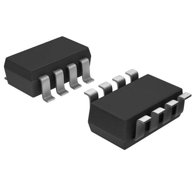
| 产品图片 |
|
| rohs | 符合RoHS无铅 / 符合限制有害物质指令(RoHS)规范要求 |
| 产品系列 | 放大器 IC,运算放大器 - 运放,Texas Instruments OPA4727AIPWRe-trim™ |
| 数据手册 | |
| 产品型号 | OPA4727AIPWR |
| 产品种类 | 运算放大器 - 运放 |
| 供应商器件封装 | 14-TSSOP |
| 共模抑制比—最小值 | 86 dB |
| 关闭 | No Shutdown |
| 其它名称 | 296-21237-1 |
| 包装 | 剪切带 (CT) |
| 压摆率 | 30 V/µs |
| 双重电源电压 | +/- 3 V, +/- 5 V |
| 商标 | Texas Instruments |
| 增益带宽生成 | 20 MHz |
| 增益带宽积 | 20MHz |
| 安装类型 | 表面贴装 |
| 安装风格 | SMD/SMT |
| 封装 | Reel |
| 封装/外壳 | 14-TSSOP(0.173",4.40mm 宽) |
| 封装/箱体 | TSSOP-14 |
| 工作温度 | -40°C ~ 125°C |
| 工作电源电压 | 4 V to 12 V, +/- 2 V to +/- 6 V |
| 工厂包装数量 | 2000 |
| 技术 | CMOS |
| 放大器类型 | 通用 |
| 最大双重电源电压 | +/- 6 V |
| 最大工作温度 | + 125 C |
| 最小双重电源电压 | +/- 2 V |
| 最小工作温度 | - 40 C |
| 标准包装 | 1 |
| 电压-电源,单/双 (±) | 4 V ~ 12 V, ±2 V ~ 6 V |
| 电压-输入失调 | 15µV |
| 电流-电源 | 4.3mA |
| 电流-输入偏置 | 85pA |
| 电流-输出/通道 | 40mA |
| 电源电流 | 6.5 mA |
| 电路数 | 4 |
| 系列 | OPA4727 |
| 设计资源 | http://www.digikey.com/product-highlights/cn/zh/texas-instruments-webench-design-center/3176 |
| 转换速度 | 30 V/us |
| 输入偏压电流—最大 | 500 pA |
| 输入参考电压噪声 | 10 nV |
| 输入补偿电压 | 175 uV |
| 输出电流 | 40 mA |
| 输出类型 | 满摆幅 |
| 通道数量 | 4 Channel |


- 商务部:美国ITC正式对集成电路等产品启动337调查
- 曝三星4nm工艺存在良率问题 高通将骁龙8 Gen1或转产台积电
- 太阳诱电将投资9.5亿元在常州建新厂生产MLCC 预计2023年完工
- 英特尔发布欧洲新工厂建设计划 深化IDM 2.0 战略
- 台积电先进制程称霸业界 有大客户加持明年业绩稳了
- 达到5530亿美元!SIA预计今年全球半导体销售额将创下新高
- 英特尔拟将自动驾驶子公司Mobileye上市 估值或超500亿美元
- 三星加码芯片和SET,合并消费电子和移动部门,撤换高东真等 CEO
- 三星电子宣布重大人事变动 还合并消费电子和移动部门
- 海关总署:前11个月进口集成电路产品价值2.52万亿元 增长14.8%


PDF Datasheet 数据手册内容提取
(cid:2)(cid:17)(cid:14)(cid:14)(cid:20)(cid:2)(cid:14)(cid:13)(cid:18)(cid:12) (cid:4)(cid:14)(cid:13)(cid:8)(cid:17)(cid:7)(cid:16)(cid:15) OPA727 OPA2727 (cid:10)(cid:14)(cid:13)(cid:11) (cid:5)(cid:9)(cid:19)(cid:6)(cid:15) (cid:3)(cid:12)(cid:15)(cid:16)(cid:14)(cid:17)(cid:11)(cid:9)(cid:12)(cid:16)(cid:15) OPA4727 OPA2727 ,, OPA727 OPA728 OPA4727, OPA728 OPA2727 OPA727 OPA728 SBOS314H–SEPTEMBER2004–REVISEDAPRIL2007 e-trim™ 20MHz, High Precision CMOS Operational Amplifier FEATURES DESCRIPTION • OFFSET:15m V(typ),150m V(max) The OPA727 and OPA728 series op amps use a • DRIFT:0.3m V/(cid:176) C(typ),1.5m V/(cid:176) C(max) state-of-the-art 12V analog CMOS process and • BANDWIDTH:20MHz e-trim, a package-level trim, offering outstanding dc precision and ac performance. The extremely low • SLEWRATE:30V/m s offset (150m V max) and drift (1.5m V/(cid:176) C) are achieved • BIASCURRENT:500pA(max) by trimming the IC digitally after packaging to avoid • LOWNOISE:6nV/(cid:214) Hzat100kHz the shift in parameters as a result of stresses during package assembly. To correct for offset drift, the • THD+N:0.0003%at1kHz OPA727 and OPA728 family is trimmed over • QUIESCENTCURRENT:4.3mA/ch temperature. The devices feature very high CMRR • SUPPLYVOLTAGE:4Vto12V andopen-loopgaintominimizeerrors. • SHUTDOWNMODE(OPA728):6m A Excellent ac characteristics, such as 20MHz GBW, 30V/m s slew rate and 0.0003% THD+N make the APPLICATIONS OPA727 and OPA728 well-suited for communication, • OPTICALNETWORKING high-end audio, and active filter applications. With a bias current of less than 500pA, they are well suited • TRANSIMPEDANCEAMPLIFIERS for use as transimpedance (I/V-conversion) • INTEGRATORS amplifiers for monitoring optical power in ONET • ACTIVEFILTERS applications. • A/DCONVERTERDRIVERS Optimized for single-supply operation up to 12V, the • I/VCONVERTERFORDACs input common-mode range extends to GND for true • HIGHPERFORMANCEAUDIO single-supply functionality. The output swings to • PROCESSCONTROL within150mVoftherails,maximizing dynamic range. The low quiescent current of 4.3mA makes it • TESTEQUIPMENT well-suited for use in battery-operated equipment. The OPA728 shutdown version reduces the OPAx727ANDOPAx728RELATEDPRODUCTS quiescent current to typically 6m A and features a FEATURES PRODUCT reference pin for easy shutdown operation with 20MHz,3mV,4m V/(cid:176) C OPA725 standardCMOSlogicindual-supplyapplications. (non-e-trimversionofOPA727) For ease of use, the OPA727 and OPA728 op amp 20MHz,3mV,4m V/(cid:176) C,Shutdown OPA726 families are fully specified and tested over the supply (non-e-trimversionofOPA728) range of 4V to 12V. The OPA727 (single) and OPA728 (single with shutdown) are available in MSOP-8 and DFN-8; the OPA2727 (dual) is +12V available in DFN-8 and SO-8; and the quad version OPA4727inTSSOP-14.Allversionsare specified for operationfrom–40(cid:176) Cto+125(cid:176) C. OPA727 V l OUT -V B Pleasebeawarethatanimportantnoticeconcerningavailability,standardwarranty,anduseincriticalapplicationsofTexas Instrumentssemiconductorproductsanddisclaimerstheretoappearsattheendofthisdatasheet. e-trimisatrademarkofTexasInstruments. Allothertrademarksarethepropertyoftheirrespectiveowners. PRODUCTIONDATAinformationiscurrentasofpublicationdate. Copyright©2004–2007,TexasInstrumentsIncorporated Products conform to specifications per the terms of the Texas Instruments standard warranty. Production processing does not necessarilyincludetestingofallparameters.
OPA727,, OPA2727 OPA4727, OPA728 www.ti.com SBOS314H–SEPTEMBER2004–REVISEDAPRIL2007 This integrated circuit can be damaged by ESD. Texas Instruments recommends that all integrated circuits be handled with appropriateprecautions.Failuretoobserveproperhandlingandinstallationprocedurescancausedamage. ESD damage can range from subtle performance degradation to complete device failure. Precision integrated circuits may be more susceptible to damage because very small parametric changes could cause the device not to meet its published specifications. PACKAGE/ORDERINGINFORMATION(1) PRODUCT PACKAGE-LEAD PACKAGEDESIGNATOR PACKAGEMARKING Non-Shutdown MSOP-8 DGK AUE OPA727 DFN-8 DRB NSF DFN-8 DRB NSD OPA2727 SO-8 D O2727A OPA4727 TSSOP-14 PW OPA4727 Shutdown MSOP-8 DGK AUF OPA728 DFN-8 DRB NSG (1) ForthemostcurrentpackageandorderinginformationseethePackageOptionAddendumattheendofthisdocument,orseetheTI websiteatwww.ti.com. ABSOLUTE MAXIMUM RATINGS(1) OPA727,OPA2727 OPA4727,OPA728 UNIT SupplyVoltage +13.2 V Voltage(2) –0.5to(V+)+0.5 V SignalInputTerminals Current(2) – 10 mA OutputShort-Circuit(3) Continuous OperatingTemperature –55to+125 (cid:176) C StorageTemperature –55to+150 (cid:176) C JunctionTemperature +150 (cid:176) C HumanBodyModel 2000 V ESDRating ChargedDeviceModel 1000 V (1) Stressesabovetheseratingsmaycausepermanentdamage.Exposuretoabsolutemaximumconditionsforextendedperiodsmay degradedevicereliability.Thesearestressratingsonly,andfunctionaloperationofthedeviceattheseoranyotherconditionsbeyond thosespecifiedisnotsupported. (2) Inputterminalsarediode-clampedtothepower-supplyrails.Inputsignalsthatcanswingmorethan0.5Vbeyondthesupplyrailsshould becurrentlimitedto10mAorless. (3) Short-circuittoground,oneamplifierperpackage. 2 SubmitDocumentationFeedback
OPA727,, OPA2727 OPA4727, OPA728 www.ti.com SBOS314H–SEPTEMBER2004–REVISEDAPRIL2007 PIN CONFIGURATIONS OPA727 OPA2727 MSOP-8 SO-8 (TOPVIEW) (TOPVIEW) NC(1) 1 8 NC(1) OUT A 1 8 V+ -IN 2 7 V+ -IN A 2 A 7 OUT B +IN 3 6 OUT +IN A 3 B 6 -IN B (1) V- 4 5 NC V- 4 5 +IN B OPA727 OPA2727 DFN-8 DFN-8 (TOPVIEW) (TOPVIEW) NC(1) 1 8 NC(1) OUT A 1 8 V+ Exposed Exposed -IN 2 Thermal 7 V+ -IN A 2 Thermal 7 OUT B Die Pad Die Pad +VIN- 34 Undeornside(2) 65 ONCU(T1) +INV A- 34 Undeornside(2) 65 -+IINN BB OPA728 OPA4727 MSOP-8 TSSOP-14 (TOPVIEW) (TOPVIEW) REF(3) 1 8 Enable OUT A 1 14 OUT D -IN 2 7 V+ -IN A 2 A D 13 -IN D +IN 3 6 OUT +IN A 3 12 +IN D (1) V- 4 5 NC V+ 4 11 V- +IN B 5 10 +IN C OPA728 DFN-8 -IN B 6 B C 9 -IN C (TOPVIEW) OUT B 7 8 OUT C REF(3) 1 8 Enable Exposed -IN 2 Thermal 7 V+ Notes: Die Pad 1. NCdenotesnointernalconnection. +IN 3 on 6 OUT Underside(2) (1) 2. ConnectthermaldiepadtoV–. V- 4 5 NC 3. REFisthereferencevoltageforENABLEpin. SubmitDocumentationFeedback 3
OPA727,, OPA2727 OPA4727, OPA728 www.ti.com SBOS314H–SEPTEMBER2004–REVISEDAPRIL2007 ELECTRICAL CHARACTERISTICS: V = +4V to +12V or V = – 2V to – 6V S S Boldfacelimitsapplyoverthespecifiedtemperaturerange,T =–40(cid:176) Cto+125(cid:176) C. A AtT =+25(cid:176) C,R =10kW connectedtoV /2,andV =V /2,unlessotherwisenoted. A L S OUT S OPA727,OPA728, OPA2727,OPA4727 PARAMETER CONDITIONS MIN TYP MAX UNIT OFFSETVOLTAGE InputOffsetVoltage VOS VS=– 5V,VCM=0V OPA727DFN,OPA728DFNPackages 15 150 m V OPA727MSOP,OPA728MSOPPackages 15 300 m V OPA2727 15 150 m V OPA4727 15 175 m V Drift dVOS/dT 0(cid:176)Cto+85(cid:176)C 0.3 1.5 m V/(cid:176)C –40(cid:176)Cto+125(cid:176)C 0.6 3 m V/(cid:176)C vsPowerSupply PSRR VS=– 2Vto– 6V,VCM=V– 30 150 m V/V OverTemperature VS=– 2Vto– 6V,VCM=V– 150 m V/V ChannelSeparation,dc 1 m V/V INPUTBIASCURRENT InputBiasCurrent – 85 – 500 pA OverTemperature SeeTypicalCharacteristics InputOfsetCurrent IOS – 10 – 100 pA NOISE InputVoltageNoise,f=0.1Hzto10Hz en VS=– 6V,VCM=0V 10 m VPP InputVoltageNoiseDensity,f=10kHz en VS=– 6V,VCM=0V 10 nV/(cid:214) Hz InputVoltageNoiseDensity,f=100kHz en VS=– 6V,VCM=0V 6 nV/(cid:214) Hz InputCurrentNoiseDensity,f=1kHz in VS=– 6V,VCM=0V 2.5 fA/(cid:214) Hz INPUTVOLTAGERANGE Common-ModeVoltageRange VCM (V–) (V+)–2.5 V Common-ModeRejectionRatio CMRR (V–)£ VCM£ (V+)–2.5V 86 94 dB OverTemperature (V–)£ VCM£ (V+)–2.5V 84 dB (V–)£ VCM£ (V+)–3V 94 100 dB OverTemperature (V–)£ VCM£ (V+)–3V 84 dB INPUTIMPEDANCE Differential 1011||5 W ||pF Common-Mode 1011||4 W ||pF OPEN-LOOPGAIN Open-LoopVoltageGain AOL RL=100kW ,–00..1155VV<VO<(V+) 110 120 dB OverTemperature RL=100kW ,0.15V<VO<(V+) 100 dB –0.15V RL=1kW ,0.25V<VO<(V+)–0.25V 106 116 dB OverTemperature,OPA727,OPA728 RL=1kW ,0.25V<VO<(V+)–0.25V 96 dB OverTemperature,OPA2727,OPA4727 RL=1kW ,0.35V<VO<(V+)–0.35V 96 dB FREQUENCYRESPONSE CL=20pF Gain-BandwidthProduct GBW 20 MHz SlewRate SR G=+1 30 V/m s SettlingTime,0.1% ts VS=– 6V,5VStep,G=+1 350 ns SettlingTime, 0.01% VS=±6V,5VStep,G=+1 450 ns OverloadRecoveryTime VIN· Gain>VS 50 ns TotalHarmonicDistortion+Noise THD+N VS=– 6V,VOUT=2VRMS,RL=600W , 0.003 % G=+1,f=1kHz 4 SubmitDocumentationFeedback
OPA727,, OPA2727 OPA4727, OPA728 www.ti.com SBOS314H–SEPTEMBER2004–REVISEDAPRIL2007 ELECTRICAL CHARACTERISTICS: V = +4V to +12V or V = – 2V to – 6V (continued) S S Boldfacelimitsapplyoverthespecifiedtemperaturerange,T =–40(cid:176) Cto+125(cid:176) C. A AtT =+25(cid:176) C,R =10kW connectedtoV /2,andV =V /2,unlessotherwisenoted. A L S OUT S OPA727,OPA728, OPA2727,OPA4727 PARAMETER CONDITIONS MIN TYP MAX UNIT OUTPUT VoltageOutputSwingfromRail RL=100kW ,AOL>110dB 100 150 mV OverTemperature RL=100kW ,AOL>100dB 150 mV RL=1kW ,AOL>106dB 200 250 mV OverTemperature,OPA727,OPA728 RL=1kW ,AOL>96dB 250 mV OverTemperature,OPA2727,OPA4727 RL=1kW ,AOL>96dB 350 mV OutputCurrent IOUT |VS–VOUT|<1V 40 mA Short-CircuitCurrent ISC – 55 mA CapacitiveLoadDrive CLOAD SeeTypicalCharacteristics Open-LoopOutputImpedance f=1MHz,IO=0 40 W ENABLE/SHUTDOWN(OPA728) tOFF 5 m s tON 80 m s EnableReference(RefPin)VoltageRange V– (V+)–2 V VL(amplifierisdisabled) <VDGND+0.8V V VH(amplifierisenabled) >VDGND+2V V InputBiasCurrentofEnablePin 5 pA IQSD AmplifierDisabled 6 15 m A POWERSUPPLY SpecifiedVoltageRange VS 4 12 V 3.5to OperatingVoltageRange VS 13.2 V QuiescentCurrent(peramplifier) IQ 4.3 6.5 mA OverTemperature 6.5 mA TEMPERATURERANGE SpecifiedRange –40 +125 (cid:176)C OperatingRange –55 +125 (cid:176)C StorageRange –55 +150 (cid:176)C ThermalResistance q JA MSOP-8,SO-8 150 (cid:176)C/W TSSOP-14 100 (cid:176)C/W DFN-8 46 (cid:176)C/W SubmitDocumentationFeedback 5
OPA727,, OPA2727 OPA4727, OPA728 www.ti.com SBOS314H–SEPTEMBER2004–REVISEDAPRIL2007 TYPICAL CHARACTERISTICS AtT =+25(cid:176) C,V =– 6V,R =10kW connectedtoV /2,andV =V /2,unlessotherwisenoted. A S L S OUT S GAINANDPHASEvsFREQUENCY COMMON-MODEREJECTIONRATIOvsFREQUENCY 180 180 120 160 160 140 140 100 120 120 ain(dB) 18000 Phase 18000 °hase() RR(dB) 8600 G 60 60 P M C 40 Gain 40 40 20 20 0 0 20 –20 –20 (V–)£VCM£(V+)–2V 10 100 1k 10k 100k 1M 10M 100M 0 10 100 1k 10k 100k 1M 10M Frequency(Hz) Frequency(Hz) Figure1. Figure2. POWER-SUPPLYREJECTIONRATIOvsFREQUENCY MAXIMUMOUTPUTVOLTAGEvsFREQUENCY 100 7 V =±6V 90 S 6 80 70 5 dB) 60 e(V) 4 R( 50 ud PSR 40 mplit 3 30 A 2 Indicatesmaximumoutput fornovisibledistortion. 20 1 10 0 0 100 1k 10k 100k 1M 10M 100M 10k 100k 1M 10M Frequency(Hz) Frequency(Hz) Figure3. Figure4. INPUTVOLTAGENOISESPECTRALDENSITY CHANNELSEPARATIONvsFREQUENCY vsFREQUENCY 140 1000 120 on(dB) 100 ÖV/Hz) 100 eparati 80 oise(n S N el e n 60 g 10 n a Cha Volt 40 20 1 1k 10k 100k 1M 10M 100M 10 100 1k 10k 100k 1M 10M Frequency(Hz) Frequency(Hz) Figure5. Figure6. 6 SubmitDocumentationFeedback
OPA727,, OPA2727 OPA4727, OPA728 www.ti.com SBOS314H–SEPTEMBER2004–REVISEDAPRIL2007 TYPICAL CHARACTERISTICS (continued) AtT =+25(cid:176) C,V =– 6V,R =10kW connectedtoV /2,andV =V /2,unlessotherwisenoted. A S L S OUT S INPUTBIASCURRENT vsCOMMON-MODEVOLTAGE OFFSETCURRENTvsTEMPERATURE 100k 10k +125°C 10k +85°C 1k A) 1k (p 100 +25°C 100 nt e utBiasCurr –1–101000 +25°C IB<±10pA I(pA)OS 101 p In –1k +85°C 0.1 –10k +125°C –100k 0.01 –6 –4 –2 0 2 4 6 –50 –25 0 25 50 75 100 125 150 Common--ModeVoltage(V) Temperature(°C) Figure7. Figure8. OPEN-LOOPGAINvsTEMPERATURE POWER-SUPPLYREJECTIONRATIOvsTEMPERATURE 140 120 130 R =100kW L 120 100 B) dB) (dOL 110 RR( A RL=1kW PS 100 80 90 80 60 –50 –25 0 25 50 75 100 125 150 –50 –25 0 25 50 75 100 125 150 Temperature(°C) Temperature(°C) Figure9. Figure10. COMMON-MODEREJECTIONRATIOvsTEMPERATURE QUIESCENTCURRENTvsTEMPERATURE 110 5 100 4 B) 90 3 (d A) R m MR 80 I(Q 2 C 70 1 (V–)£V £(V+)–2V CM 60 0 –50 –25 0 25 50 75 100 125 150 –50 –25 0 25 50 75 100 125 150 Temperature(°C) Temperature(°C) Figure11. Figure12. SubmitDocumentationFeedback 7
OPA727,, OPA2727 OPA4727, OPA728 www.ti.com SBOS314H–SEPTEMBER2004–REVISEDAPRIL2007 TYPICAL CHARACTERISTICS (continued) AtT =+25(cid:176) C,V =– 6V,R =10kW connectedtoV /2,andV =V /2,unlessotherwisenoted. A S L S OUT S QUIESCENTCURRENTvsSUPPLYVOLTAGE SHORT-CIRCUITCURRENTvsTEMPERATURE 5.0 90 4.8 80 Sourcing 4.6 70 mA) 4.4 A) 60 ( m mplifier 44..20 Circuit( 5400 Sinking perA 33..86 Short-- 30 Q I 20 3.4 3.2 10 3.0 0 3 4 5 6 7 8 9 10 11 12 13 14 –50 –25 0 25 50 75 100 125 150 SupplyVoltage(V) Temperature(°C) Figure13. Figure14. SHORT-CIRCUITCURRENTvsSUPPLYVOLTAGE OUTPUTVOLTAGESWINGvsOUTPUTCURRENT 90 6 Sourcing –40°C 80 4 A) 70 m nt( 60 (V) 2 urre 50 Sinking age 125°C 25°C C olt 0 ort--Circuit 4300 OutputV –2 h 20 S –4 10 –40°C 0 –6 5 5 5 5 5 5 5 5 5 5 5 0 10 20 30 40 50 60 70 80 3. 4. 5. 6. 7. 8. 9. 0. 1. 2. 3. 1 1 1 1 OutputCurrent(mA) Supply Voltage(V) Figure15. Figure16. TOTALHARMONICDISTORTION+NOISEvs FREQUENCY SETTLINGTIMEvsGAIN 0.01 5000 R = 600W L V = 2Vrms 4500 OUT BW = 80kHz 4000 %) s) 3500 Noise( 0.001 Time(n 32050000 HD+ ettling 2000 T S 1500 0.01% 1000 0.1% 500 0.0001 0 10 100 1k 10k 100k 1 10 100 Frequency(Hz) NoninvertingGain(V/V) Figure17. Figure18. 8 SubmitDocumentationFeedback
OPA727,, OPA2727 OPA4727, OPA728 www.ti.com SBOS314H–SEPTEMBER2004–REVISEDAPRIL2007 TYPICAL CHARACTERISTICS (continued) AtT =+25(cid:176) C,V =– 6V,R =10kW connectedtoV /2,andV =V /2,unlessotherwisenoted. A S L S OUT S SMALL-SIGNALOVERSHOOTvsCAPACITIVELOAD OFFSETVOLTAGEPRODUCTIONDISTRIBUTION 90 V =±5V S 80 70 %) 60 G=+1 n ( o ot 50 ati ersho 40 Popul Ov 30 G =–1 C = 3pF F 20 10 G = +5 C = 1pF F 0 10 100 1000 –150–140–130–120–110–100–90–80–70–60–50–40–30–20–100102030405060708090100110120130140150 CapacitiveLoad(pF) Offset Voltage (mV) Figure19. Figure20. OFFSETVOLTAGEDRIFTPRODUCTIONDISTRIBUTION OFFSETVOLTAGEDRIFTPRODUCTIONDISTRIBUTION (0(cid:176) CTO+85(cid:176) C) (–40(cid:176) CTO+125(cid:176) C) V =±5V V =±5V S S n n o o ati ati ul ul p p o o P P 0 0.1 0.2 0.3 0.4 0.5 0.6 0.7 0.8 0.9 1.0 1.1 1.2 1.3 1.4 1.5 00.10.20.30.40.50.60.70.80.91.01.11.21.31.41.51.61.71.81.92.02.12.22.32.42.52.62.72.82.93.0 OffsetVoltageDrift(mV/°C) OffsetVoltageDrift(mV/°C) Figure21. Figure22. OFFSETVOLTAGEvsTEMPERATURE SMALL-SIGNALSTEPRESPONSE 300 V =± 5V G = +1 S R = 10kW L 200 C = 20pF L 4s V) 100 mge ( div olta 0 mV/ V 0 et 1 Offs –100 4s –200 7RepresentativeUnitsShown –300 –50 –25 0 25 50 75 100 125 100ns/div Temperature(°C) Figure23. Figure24. SubmitDocumentationFeedback 9
OPA727,, OPA2727 OPA4727, OPA728 www.ti.com SBOS314H–SEPTEMBER2004–REVISEDAPRIL2007 TYPICAL CHARACTERISTICS (continued) AtT =+25(cid:176) C,V =– 6V,R =10kW connectedtoV /2,andV =V /2,unlessotherwisenoted. A S L S OUT S LARGE-SIGNALSTEPRESPONSE SMALL-SIGNALSTEPRESPONSE G = +1 CF= 2pF CF= 3pF R = 10kW L C = 20pF L C = 4pF F v v di 1V/di 10mV/ 10RCkFFW G =–1 10kW OPA727 CL 20pF 400ns/div 200ns/div Figure25. Figure26. LARGE-SIGNALSTEPRESPONSE CF v 4pF G =–1 di 1V/ 10RkF"W 10kW OPA727 CL 20pF 400ns/div Figure27. 10 SubmitDocumentationFeedback
OPA727,, OPA2727 OPA4727, OPA728 www.ti.com SBOS314H–SEPTEMBER2004–REVISEDAPRIL2007 APPLICATIONS INFORMATION Common-mode rejection is excellent throughout the The OPA727 and OPA728 family of op amps use input voltage range from V– to (V+) – 3V. CMRR e-trim, an adjustment to offset voltage and decreases somewhat as the common-mode voltage temperature drift made during the final steps of extends to (V+) – 2.5V, but remains very good and is manufacturing after the plastic molding is completed. tested throughout this range. See the Electrical This compensates for performance shifts that can Characteristicstablefordetails. occur during the molding process. Through e-trim, the OPA727 and OPA728 deliver excellent offset voltage (150m V max) and extremely low offset a) Single-Supply Configuration voltage drift (1.5m V/(cid:176) C). Additionally, these 20MHz Enable +12V CMOSopampshaveafastslewrate,lownoise, and Digital excellent PSRR, CMRR, and AOL. They can operate Logic ontypically4.3mAquiescentcurrentfromasingle(or OPA728 V split) supply in the range of 4V to 12V (– 2V to – 6V), OUT REF making them highly versatile and easy to use. They arestableinaunity-gainconfiguration. VREF= DGND Power-supply pins should be bypassed with 1nF ceramic capacitors in parallel with 1m F tantalum capacitors. b) Dual-Supply Configuration OPERATING VOLTAGE Enable +5V Digital OPA727 series op amps are specified from 4V to Logic 12V supplies over a temperature range of –40(cid:176) C to OPA728 V +125(cid:176) C. They will operate well in – 5V or +5V to OUT +12V power-supply systems. Parameters that vary REF significantly with operating voltage or temperature V = DGND REF -5V areshownintheTypicalCharacteristics. ENABLE/SHUTDOWN Figure28.EnableReferencePinConnectionfor OPA727 series op amps require approximately Single-andDual-SupplyConfigurations 4.3mA quiescent current. The enable/shutdown feature of the OPA728 allows the op amp to be shut offtoreducethiscurrenttoapproximately6m A. INPUT OVER-VOLTAGE PROTECTION The enable/shutdown input is referenced to the Device inputs are protected by ESD diodes that will EnableReferencePin, REF (see Pin Configurations). conduct if the input voltages exceed the power This pin can be connected to logic ground in supplies by more than approximately 300mV. dual-supply op amp configurations to avoid Momentary voltages greater than 300mV beyond the level-shifting the enable logic signal, as shown in power supply can be tolerated if the current is limited Figure28. to 10mA. This is easily accomplished with an input resistor in series with the op amp, as shown in The Enable Reference Pin voltage, V , must not REF Figure 29. The OPA727 series features no phase exceed (V+) – 2V. It may be set as low as V–. The inversion when the inputs extend beyond supplies, if amplifier is enabled when the Enable Pin voltage is theinputiscurrentlimited. greater than V + 2V. The amplifier is disabled REF (shutdown) if the Enable Pin voltage is less than V + 0.8V. The Enable Pin is connected to internal REF V+ pull-up circuitry and will enable the device if left I OVERLOAD unconnected. 10mA max COMMON-MODE VOLTAGE RANGE R OPA727 VOUT V IN The input common-mode voltage range of the V- OPA727 and OPA728 series extends from V– to (V+)–2.5V. Figure29.InputCurrentProtectionforVoltages ExceedingtheSupplyVoltage SubmitDocumentationFeedback 11
OPA727,, OPA2727 OPA4727, OPA728 www.ti.com SBOS314H–SEPTEMBER2004–REVISEDAPRIL2007 RAIL-TO-RAIL OUTPUT +5V +5V A class AB output stage with common-source transistors is used to achieve rail-to-rail output. This 75W output stage is capable of driving heavy loads VIN OPA727 AINADS8342 connected to any point between V+ and V–. For light ±2.5V 330pF 16-Bit ADC resistive loads (>100kW ), the output voltage can -5V Common swing to 150mV from the supply rail, while still maintaining excellent linearity (A > 110dB). With OL -5V 1kW resistive loads, the output is specified to swing to within 250mV from the supply rails with excellent Figure31.OPA727DrivinganADC linearity (see the Typical Characteristics curve, OutputVoltageSwingvsOutputCurrent). TRANSIMPEDANCE AMPLIFIER CAPACITIVE LOAD AND STABILITY Wide bandwidth, low input bias current, and low Capacitive load drive is dependent upon gain and inputvoltageandcurrent noise make the OPA727 an the overshoot requirements of the application. idealwideband photodiode transimpedance amplifier. Increasing the gain enhances the ability of the Low-voltage noise is important because photodiode amplifier to drive greater capacitive loads (see the capacitance causes the effective noise gain of the Typical Characteristics curve, Small-Signal circuittoincreaseathighfrequency. OvershootvsCapacitiveLoad). The key elements to a transimpedance design, as One method of improving capacitive load drive in the shown in Figure 32, are the expected diode unity-gain configuration is to insert a 10W to 20W capacitance (C ), which should include the parasitic D resistor inside the feedback loop, as shown in input common-mode and differential-mode input Figure 30. This reduces ringing with large capacitive capacitance(4pF+5pFfortheOPA727); the desired loadswhilemaintainingDCaccuracy. transimpedance gain (R ); and the GBW for the F OPA727(20MHz).Withthesethreevariables set, the feedback capacitor value (C ) can be set to control V+ F the frequency response. C includes the stray R F 20SW capacitance of RF, which is 0.2pF for a typical OPA727 V surface-mountresistor. OUT V IN C R L L (1) C F < 1pF Figure30.SeriesResistorinUnity-GainBuffer ConfigurationImprovesCapacitiveLoadDrive RF 10MW DRIVING FAST 16-BIT ADCs The OPA727 series is optimized for driving fast +5V 16-bit ADCs such as the ADS8342. The OPA727 op amps buffer the converter input capacitance and l resultingchargeinjection, while providing signal gain. CD OPA727 VOUT Figure 31 shows the OPA727 in a single-ended method of interfacing to the ADS8342 16-bit, -5V 250kSPS, 4-channel ADC with an input range of – 2.5V. The OPA727 has demonstrated excellent settling time to the 16-bit level within the 600ns NOTE: (1) C is optional to prevent gain peaking. F acquisition time of the ADS8342. The RC filter, It includes the stray capacitance ofR . F showninFigure31,hasbeencarefully tuned for best noise and settling performance. It may need to be Figure32.Dual-SupplyTransimpedance adjusted for different op amp configurations. Refer to Amplifier the ADS8342 data sheet (available for download at www.ti.com) for additional information on this product. 12 SubmitDocumentationFeedback
OPA727,, OPA2727 OPA4727, OPA728 www.ti.com SBOS314H–SEPTEMBER2004–REVISEDAPRIL2007 To achieve a maximally-flat, 2nd-order Butterworth For additional information, refer to Application frequency response, the feedback pole should be set Bulletin (SBOA055), Compensate Transimpedance to: Amplifiers Intuitively, available for download at www.ti.com. 1 (cid:2) GBW 2(cid:1)R C (cid:1) 4(cid:1)R C F F F D (1) OPTIMIZING THE TRANSIMPEDANCE CIRCUIT Bandwidthiscalculatedby: To achieve the best performance, components (cid:3) GBW f(cid:1)3dB(cid:2) 2(cid:1)R C Hz should be selected according to the following F D (2) guidelines: 1. For lowest noise, select R to create the total For even higher transimpedance bandwidth, the F required gain. Using a lower value for R and high-speed CMOS OPA380 (90MHz GBW), OPA354 F adding gain after the transimpedance amplifier (100MHz GBW), OPA300 (180MHz GBW), OPA355 generally produces poorer noise performance. (200MHz GBW), or OPA656, OPA657 (400MHz The noise produced by R increases with the GBW)maybeused. F square-root of R , whereas the signal F For single-supply applications, the +IN input can be increases linearly. Therefore, signal-to-noise biased with a positive dc voltage to allow the output ratio is improved when all the required gain is to reach true zero when the photodiode is not placedinthetransimpedancestage. exposed to any light, and respond without the added 2. Minimize photodiode capacitance and stray delay that results from coming out of the negative capacitance at the summing junction (inverting rail; this is shown in Figure 33. This bias voltage also input). This capacitance causes the voltage appears across the photodiode, providing a reverse noise of the op amp to be amplified biasforfasteroperation. (increasing amplification at high frequency). Using a low-noise voltage source to (1) reverse-bias a photodiode can significantly C F < 1pF reduce its capacitance. Smaller photodiodes have lower capacitance. Use optics to concentratelightonasmallphotodiode. 3. Noise increases with increased bandwidth. RF Limit the circuit bandwidth to only that 10MW required. Use a capacitor across the R to F limit bandwidth, even if not required for stability. 4. Circuit board leakage can degrade the V+ performance of an otherwise well-designed l amplifier. Clean the circuit board carefully. A OPA727 V circuit board guard trace that encircles the OUT +V summing junction and is driven at the same Bias voltagecanhelpcontrolleakage. For additional information, refer to the Application Bulletins Noise Analysis of FET Transimpedance NOTE: (1) C is optional to prevent gain peaking. Amplifiers (SBOA060), and Noise Analysis for F It includes the stray capacitance ofRF. High-Speed Op Amps (SBOA066), available for downloadattheTIwebsite. Figure33.Single-SupplyTransimpedance Amplifier SubmitDocumentationFeedback 13
OPA727,, OPA2727 OPA4727, OPA728 www.ti.com SBOS314H–SEPTEMBER2004–REVISEDAPRIL2007 C 3 C 2.2nF 1 1nF R R 3 4 1/2 R1 R2 1/2 2.07kW 22.3kW OPA2727 VO 1.93kW 15.9kW OPA2727 C 4 C 100pF 2 330pF DC Gain = 1 Cutoff Frequency = 50kHz Note: FilterProisalow-passfilterdesignprogramavailablefordownloadatnocostfromTI’swebsite(www.ti.com).The programcanbeusedtodeterminecomponentvaluesforothercutofffrequenciesorfiltertypes. Figure34.Four-PoleButterworthSallen-KeyLow-PassFilter DFN PACKAGE LAYOUT GUIDELINES The OPA727 series uses the DFN-8 (also known as The leadframe die pad should be soldered to a SON),whichisaQFNpackagewith lead contacts on thermal pad on the PCB. A mechanical data sheet only two sides of the bottom of the package. This showing an example layout is attached at the end of leadless, near-chip-scale package maximizes board this data sheet. Refinements to this layout may be space and enhances thermal and electrical required based on assembly process requirements. characteristicsthroughanexposedpad. Mechanical drawings located at the end of this data sheet list the physical dimensions for the package DFN packages are physically small, have a smaller and pad. The five holes in the landing pattern are routing area, improved thermal performance, and optional, and are intended for use with thermal vias improved electrical parasitics, with a pinout scheme that connect the leadframe die pad to the heatsink that is consistent with other commonly-used areaonthePCB. packages, such as SO and MSOP. Additionally, the absence of external leads eliminates bent-lead Soldering the exposed pad significantly improves issues. board-level reliability during temperature cycling, key push, package shear, and similar board-level tests. The DFN package can be easily mounted using Even with applications that have low-power standard printed circuit board (PCB) assembly dissipation, the exposed pad must be soldered to the techniques. See Application Note, QFN/SON PCB PCB to provide structural integrity and long-term Attachment (SLUA271) and Application Report, reliability. Quad Flatpack No-Lead Logic Packages (SCBA017), bothavailablefordownloadatwww.ti.com. The exposed leadframe die pad on the bottom of thepackageshouldbeconnectedtoV–. 14 SubmitDocumentationFeedback
PACKAGE OPTION ADDENDUM www.ti.com 24-Aug-2018 PACKAGING INFORMATION Orderable Device Status Package Type Package Pins Package Eco Plan Lead/Ball Finish MSL Peak Temp Op Temp (°C) Device Marking Samples (1) Drawing Qty (2) (6) (3) (4/5) OPA2727AID ACTIVE SOIC D 8 75 Green (RoHS CU NIPDAU Level-3-260C-168 HR -40 to 85 O2727A & no Sb/Br) 2727A OPA2727AIDR ACTIVE SOIC D 8 2500 Green (RoHS CU NIPDAU Level-3-260C-168 HR -40 to 85 O2727A & no Sb/Br) 2727A OPA2727AIDRBR ACTIVE SON DRB 8 2500 Green (RoHS CU NIPDAU Level-3-260C-168 HR -40 to 85 NSD & no Sb/Br) OPA2727AIDRBT ACTIVE SON DRB 8 250 Green (RoHS CU NIPDAU Level-3-260C-168 HR -40 to 85 NSD & no Sb/Br) OPA4727AIPW ACTIVE TSSOP PW 14 90 Green (RoHS CU NIPDAU Level-2-260C-1 YEAR -40 to 85 OPA4727 & no Sb/Br) OPA4727AIPWR ACTIVE TSSOP PW 14 2000 Green (RoHS CU NIPDAU Level-2-260C-1 YEAR -40 to 85 OPA4727 & no Sb/Br) OPA727AIDGKR ACTIVE VSSOP DGK 8 2500 Green (RoHS CU NIPDAU | Call TI Level-2-260C-1 YEAR -40 to 85 AUE & no Sb/Br) OPA727AIDGKRG4 ACTIVE VSSOP DGK 8 2500 Green (RoHS Call TI Level-2-260C-1 YEAR -40 to 85 AUE & no Sb/Br) OPA727AIDGKT ACTIVE VSSOP DGK 8 250 Green (RoHS CU NIPDAU | Call TI Level-2-260C-1 YEAR -40 to 85 AUE & no Sb/Br) OPA727AIDRBT ACTIVE SON DRB 8 250 Green (RoHS CU NIPDAU Level-2-260C-1 YEAR -40 to 85 NSF & no Sb/Br) OPA727AIDRBTG4 ACTIVE SON DRB 8 250 Green (RoHS CU NIPDAU Level-2-260C-1 YEAR -40 to 85 NSF & no Sb/Br) OPA728AIDGKT ACTIVE VSSOP DGK 8 250 Green (RoHS CU NIPDAUAG Level-2-260C-1 YEAR -40 to 125 AUF & no Sb/Br) OPA728AIDRBT ACTIVE SON DRB 8 250 Green (RoHS CU NIPDAU Level-2-260C-1 YEAR -40 to 125 NSG & no Sb/Br) (1) The marketing status values are defined as follows: ACTIVE: Product device recommended for new designs. LIFEBUY: TI has announced that the device will be discontinued, and a lifetime-buy period is in effect. NRND: Not recommended for new designs. Device is in production to support existing customers, but TI does not recommend using this part in a new design. PREVIEW: Device has been announced but is not in production. Samples may or may not be available. OBSOLETE: TI has discontinued the production of the device. Addendum-Page 1
PACKAGE OPTION ADDENDUM www.ti.com 24-Aug-2018 (2) RoHS: TI defines "RoHS" to mean semiconductor products that are compliant with the current EU RoHS requirements for all 10 RoHS substances, including the requirement that RoHS substance do not exceed 0.1% by weight in homogeneous materials. Where designed to be soldered at high temperatures, "RoHS" products are suitable for use in specified lead-free processes. TI may reference these types of products as "Pb-Free". RoHS Exempt: TI defines "RoHS Exempt" to mean products that contain lead but are compliant with EU RoHS pursuant to a specific EU RoHS exemption. Green: TI defines "Green" to mean the content of Chlorine (Cl) and Bromine (Br) based flame retardants meet JS709B low halogen requirements of <=1000ppm threshold. Antimony trioxide based flame retardants must also meet the <=1000ppm threshold requirement. (3) MSL, Peak Temp. - The Moisture Sensitivity Level rating according to the JEDEC industry standard classifications, and peak solder temperature. (4) There may be additional marking, which relates to the logo, the lot trace code information, or the environmental category on the device. (5) Multiple Device Markings will be inside parentheses. Only one Device Marking contained in parentheses and separated by a "~" will appear on a device. If a line is indented then it is a continuation of the previous line and the two combined represent the entire Device Marking for that device. (6) Lead/Ball Finish - Orderable Devices may have multiple material finish options. Finish options are separated by a vertical ruled line. Lead/Ball Finish values may wrap to two lines if the finish value exceeds the maximum column width. Important Information and Disclaimer:The information provided on this page represents TI's knowledge and belief as of the date that it is provided. TI bases its knowledge and belief on information provided by third parties, and makes no representation or warranty as to the accuracy of such information. Efforts are underway to better integrate information from third parties. TI has taken and continues to take reasonable steps to provide representative and accurate information but may not have conducted destructive testing or chemical analysis on incoming materials and chemicals. TI and TI suppliers consider certain information to be proprietary, and thus CAS numbers and other limited information may not be available for release. In no event shall TI's liability arising out of such information exceed the total purchase price of the TI part(s) at issue in this document sold by TI to Customer on an annual basis. Addendum-Page 2
PACKAGE MATERIALS INFORMATION www.ti.com 3-Aug-2017 TAPE AND REEL INFORMATION *Alldimensionsarenominal Device Package Package Pins SPQ Reel Reel A0 B0 K0 P1 W Pin1 Type Drawing Diameter Width (mm) (mm) (mm) (mm) (mm) Quadrant (mm) W1(mm) OPA2727AIDR SOIC D 8 2500 330.0 12.4 6.4 5.2 2.1 8.0 12.0 Q1 OPA2727AIDRBR SON DRB 8 2500 330.0 12.4 3.3 3.3 1.1 8.0 12.0 Q2 OPA2727AIDRBT SON DRB 8 250 180.0 12.4 3.3 3.3 1.1 8.0 12.0 Q2 OPA4727AIPWR TSSOP PW 14 2000 330.0 12.4 6.9 5.6 1.6 8.0 12.0 Q1 OPA727AIDGKR VSSOP DGK 8 2500 330.0 12.4 5.3 3.4 1.4 8.0 12.0 Q1 OPA727AIDGKT VSSOP DGK 8 250 180.0 12.4 5.3 3.4 1.4 8.0 12.0 Q1 OPA727AIDRBT SON DRB 8 250 180.0 12.4 3.3 3.3 1.1 8.0 12.0 Q2 OPA728AIDGKT VSSOP DGK 8 250 180.0 12.4 5.3 3.4 1.4 8.0 12.0 Q1 OPA728AIDRBT SON DRB 8 250 180.0 12.4 3.3 3.3 1.1 8.0 12.0 Q2 PackMaterials-Page1
PACKAGE MATERIALS INFORMATION www.ti.com 3-Aug-2017 *Alldimensionsarenominal Device PackageType PackageDrawing Pins SPQ Length(mm) Width(mm) Height(mm) OPA2727AIDR SOIC D 8 2500 367.0 367.0 35.0 OPA2727AIDRBR SON DRB 8 2500 367.0 367.0 35.0 OPA2727AIDRBT SON DRB 8 250 210.0 185.0 35.0 OPA4727AIPWR TSSOP PW 14 2000 367.0 367.0 35.0 OPA727AIDGKR VSSOP DGK 8 2500 367.0 367.0 35.0 OPA727AIDGKT VSSOP DGK 8 250 210.0 185.0 35.0 OPA727AIDRBT SON DRB 8 250 210.0 185.0 35.0 OPA728AIDGKT VSSOP DGK 8 250 210.0 185.0 35.0 OPA728AIDRBT SON DRB 8 250 210.0 185.0 35.0 PackMaterials-Page2
None
PACKAGE OUTLINE DRB0008B VSON - 1 mm max height SCALE 4.000 PLASTIC SMALL OUTLINE - NO LEAD 3.1 B A 2.9 PIN 1 INDEX AREA 3.1 2.9 C 1 MAX SEATING PLANE 0.05 0.08 C 0.00 EXPOSED 1.65 0.05 (0.2) TYP THERMAL PAD 4 5 2X 1.95 2.4 0.05 8 1 6X 0.65 0.35 8X 0.25 PIN 1 ID 0.5 0.1 C A B (OPTIONAL) 8X 0.3 0.05 C 4218876/A 12/2017 NOTES: 1. All linear dimensions are in millimeters. Any dimensions in parenthesis are for reference only. Dimensioning and tolerancing per ASME Y14.5M. 2. This drawing is subject to change without notice. 3. The package thermal pad must be soldered to the printed circuit board for thermal and mechanical performance. www.ti.com
EXAMPLE BOARD LAYOUT DRB0008B VSON - 1 mm max height PLASTIC SMALL OUTLINE - NO LEAD (1.65) 8X (0.6) SYMM 1 8 8X (0.3) (2.4) (0.95) 6X (0.65) 4 5 (R0.05) TYP (0.575) ( 0.2) VIA (2.8) TYP LAND PATTERN EXAMPLE SCALE:20X 0.07 MAX 0.07 MIN ALL AROUND ALL AROUND SOLDER MASK METAL METAL UNDER SOLDER MASK OPENING SOLDER MASK OPENING NON SOLDER MASK SOLDER MASK DEFINED DEFINED (PREFERRED) SOLDER MASK DETAILS 4218876/A 12/2017 NOTES: (continued) 4. This package is designed to be soldered to a thermal pad on the board. For more information, see Texas Instruments literature number SLUA271 (www.ti.com/lit/slua271). 5. Vias are optional depending on application, refer to device data sheet. If any vias are implemented, refer to their locations shown on this view. It is recommended that vias under paste be filled, plugged or tented. www.ti.com
EXAMPLE STENCIL DESIGN DRB0008B VSON - 1 mm max height PLASTIC SMALL OUTLINE - NO LEAD SYMM 8X (0.6) METAL TYP 1 8X (0.3) 8 (0.63) SYMM 6X (0.65) (1.06) 5 4 (R0.05) TYP (1.47) (2.8) SOLDER PASTE EXAMPLE BASED ON 0.125 mm THICK STENCIL EXPOSED PAD 81% PRINTED SOLDER COVERAGE BY AREA SCALE:25X 4218876/A 12/2017 NOTES: (continued) 6. Laser cutting apertures with trapezoidal walls and rounded corners may offer better paste release. IPC-7525 may have alternate design recommendations. www.ti.com
None
None
None
None
PACKAGE OUTLINE D0008A SOIC - 1.75 mm max height SCALE 2.800 SMALL OUTLINE INTEGRATED CIRCUIT C SEATING PLANE .228-.244 TYP [5.80-6.19] .004 [0.1] C A PIN 1 ID AREA 6X .050 [1.27] 8 1 2X .189-.197 [4.81-5.00] .150 NOTE 3 [3.81] 4X (0 -15 ) 4 5 8X .012-.020 B .150-.157 [0.31-0.51] .069 MAX [3.81-3.98] .010 [0.25] C A B [1.75] NOTE 4 .005-.010 TYP [0.13-0.25] 4X (0 -15 ) SEE DETAIL A .010 [0.25] .004-.010 0 - 8 [0.11-0.25] .016-.050 [0.41-1.27] DETAIL A (.041) TYPICAL [1.04] 4214825/C 02/2019 NOTES: 1. Linear dimensions are in inches [millimeters]. Dimensions in parenthesis are for reference only. Controlling dimensions are in inches. Dimensioning and tolerancing per ASME Y14.5M. 2. This drawing is subject to change without notice. 3. This dimension does not include mold flash, protrusions, or gate burrs. Mold flash, protrusions, or gate burrs shall not exceed .006 [0.15] per side. 4. This dimension does not include interlead flash. 5. Reference JEDEC registration MS-012, variation AA. www.ti.com
EXAMPLE BOARD LAYOUT D0008A SOIC - 1.75 mm max height SMALL OUTLINE INTEGRATED CIRCUIT 8X (.061 ) [1.55] SYMM SEE DETAILS 1 8 8X (.024) [0.6] SYMM (R.002 ) TYP [0.05] 5 4 6X (.050 ) [1.27] (.213) [5.4] LAND PATTERN EXAMPLE EXPOSED METAL SHOWN SCALE:8X SOLDER MASK SOLDER MASK METAL OPENING OPENING METAL UNDER SOLDER MASK EXPOSED METAL EXPOSED METAL .0028 MAX .0028 MIN [0.07] [0.07] ALL AROUND ALL AROUND NON SOLDER MASK SOLDER MASK DEFINED DEFINED SOLDER MASK DETAILS 4214825/C 02/2019 NOTES: (continued) 6. Publication IPC-7351 may have alternate designs. 7. Solder mask tolerances between and around signal pads can vary based on board fabrication site. www.ti.com
EXAMPLE STENCIL DESIGN D0008A SOIC - 1.75 mm max height SMALL OUTLINE INTEGRATED CIRCUIT 8X (.061 ) [1.55] SYMM 1 8 8X (.024) [0.6] SYMM (R.002 ) TYP [0.05] 5 4 6X (.050 ) [1.27] (.213) [5.4] SOLDER PASTE EXAMPLE BASED ON .005 INCH [0.125 MM] THICK STENCIL SCALE:8X 4214825/C 02/2019 NOTES: (continued) 8. Laser cutting apertures with trapezoidal walls and rounded corners may offer better paste release. IPC-7525 may have alternate design recommendations. 9. Board assembly site may have different recommendations for stencil design. www.ti.com
IMPORTANTNOTICEANDDISCLAIMER TIPROVIDESTECHNICALANDRELIABILITYDATA(INCLUDINGDATASHEETS),DESIGNRESOURCES(INCLUDINGREFERENCE DESIGNS),APPLICATIONOROTHERDESIGNADVICE,WEBTOOLS,SAFETYINFORMATION,ANDOTHERRESOURCES“ASIS” ANDWITHALLFAULTS,ANDDISCLAIMSALLWARRANTIES,EXPRESSANDIMPLIED,INCLUDINGWITHOUTLIMITATIONANY IMPLIEDWARRANTIESOFMERCHANTABILITY,FITNESSFORAPARTICULARPURPOSEORNON-INFRINGEMENTOFTHIRD PARTYINTELLECTUALPROPERTYRIGHTS. TheseresourcesareintendedforskilleddevelopersdesigningwithTIproducts.Youaresolelyresponsiblefor(1)selectingtheappropriate TIproductsforyourapplication,(2)designing,validatingandtestingyourapplication,and(3)ensuringyourapplicationmeetsapplicable standards,andanyothersafety,security,orotherrequirements.Theseresourcesaresubjecttochangewithoutnotice.TIgrantsyou permissiontousetheseresourcesonlyfordevelopmentofanapplicationthatusestheTIproductsdescribedintheresource.Other reproductionanddisplayoftheseresourcesisprohibited.NolicenseisgrantedtoanyotherTIintellectualpropertyrightortoanythird partyintellectualpropertyright.TIdisclaimsresponsibilityfor,andyouwillfullyindemnifyTIanditsrepresentativesagainst,anyclaims, damages,costs,losses,andliabilitiesarisingoutofyouruseoftheseresources. TI’sproductsareprovidedsubjecttoTI’sTermsofSale(www.ti.com/legal/termsofsale.html)orotherapplicabletermsavailableeitheron ti.comorprovidedinconjunctionwithsuchTIproducts.TI’sprovisionoftheseresourcesdoesnotexpandorotherwisealterTI’sapplicable warrantiesorwarrantydisclaimersforTIproducts. MailingAddress:TexasInstruments,PostOfficeBox655303,Dallas,Texas75265 Copyright©2019,TexasInstrumentsIncorporated