ICGOO在线商城 > 集成电路(IC) > 线性 - 放大器 - 仪表,运算放大器,缓冲器放大器 > TLV4112ID
 Datasheet下载
- 型号: TLV4112ID
- 制造商: Texas Instruments
- 库位|库存: xxxx|xxxx
- 要求:
| 数量阶梯 | 香港交货 | 国内含税 |
| +xxxx | $xxxx | ¥xxxx |
查看当月历史价格
查看今年历史价格
TLV4112ID产品简介:
ICGOO电子元器件商城为您提供TLV4112ID由Texas Instruments设计生产,在icgoo商城现货销售,并且可以通过原厂、代理商等渠道进行代购。 TLV4112ID价格参考¥9.35-¥19.08。Texas InstrumentsTLV4112ID封装/规格:线性 - 放大器 - 仪表,运算放大器,缓冲器放大器, 通用 放大器 2 电路 满摆幅 8-SOIC。您可以下载TLV4112ID参考资料、Datasheet数据手册功能说明书,资料中有TLV4112ID 详细功能的应用电路图电压和使用方法及教程。
TLV4112ID 是 Texas Instruments(德州仪器)推出的一款低功耗、双通道运算放大器,属于线性 - 放大器 - 仪表、运算放大器、缓冲器放大器分类。其应用场景广泛,特别适合对低功耗和小尺寸有要求的设计。以下是 TLV4112ID 的主要应用场景:

 1. 便携式电子设备
   - TLV4112ID 的低功耗特性使其非常适合用于电池供电的便携式设备,例如手持测量仪器、便携式医疗设备(如血糖仪、脉搏血氧仪)以及消费类电子产品(如智能手表和健身追踪器)。
   - 在这些应用中,低静态电流和高电源抑制比(PSRR)有助于延长电池寿命。

 2. 信号调理
   - 该器件可以用于传感器信号的放大和调理,例如温度传感器、压力传感器或加速度计的输出信号。其轨到轨输入/输出能力确保了信号在整个动态范围内的精确处理。
   - 特别适用于工业自动化、智能家居和物联网(IoT)中的数据采集系统。

 3. 音频信号处理
   - TLV4112ID 的低噪声和低失真性能使其适合用于音频信号的放大和处理,例如麦克风前置放大器或耳机驱动器。
   - 在便携式音频设备中,如蓝牙音箱或语音助手,其低功耗特性可减少能耗。

 4. 医疗设备
   - 在医疗领域,TLV4112ID 可用于心电图(ECG)、脑电图(EEG)等生物电信号的放大和滤波。其低输入偏置电流和高共模抑制比(CMRR)有助于提高信号精度。
   - 此外,它还可用于超声波设备或其他需要精密信号放大的医疗仪器。

 5. 工业控制
   - TLV4112ID 可用于工业控制系统中的信号放大和隔离,例如 PLC(可编程逻辑控制器)模块、数据采集卡或电机控制电路。
   - 其宽工作电压范围(1.8V 至 5.5V)和双通道设计为多路信号处理提供了灵活性。

 6. 汽车电子
   - 在汽车电子中,TLV4112ID 可用于车载传感器信号放大、车载娱乐系统的音频处理以及车身控制模块(BCM)中的信号调节。
   - 其小型封装(如 SOT-23 或 VSSOP)使其适合空间受限的应用场景。

 7. 通信设备
   - TLV4112ID 可用于无线通信模块中的信号放大,例如射频前端的低噪声放大或基带信号处理。
   - 它的小尺寸和低功耗特性非常适合移动通信设备。

总结来说,TLV4112ID 凭借其低功耗、轨到轨输入/输出、宽电源电压范围和高精度特性,广泛应用于便携式设备、信号调理、音频处理、医疗设备、工业控制、汽车电子和通信设备等领域。
| 参数 | 数值 |
| -3db带宽 | - |
| 产品目录 | 集成电路 (IC)半导体 |
| 描述 | IC OPAMP GP 2.7MHZ RRO 8SOIC运算放大器 - 运放 High-Output-Drive Op Amp |
| 产品分类 | Linear - Amplifiers - Instrumentation, OP Amps, Buffer Amps集成电路 - IC |
| 品牌 | Texas Instruments |
| 产品手册 | |
| 产品图片 |
|
| rohs | 符合RoHS无铅 / 符合限制有害物质指令(RoHS)规范要求 |
| 产品系列 | 放大器 IC,运算放大器 - 运放,Texas Instruments TLV4112ID- |
| 数据手册 | |
| 产品型号 | TLV4112ID |
| 产品目录页面 | |
| 产品种类 | 运算放大器 - 运放 |
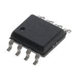
| 供应商器件封装 | 8-SOIC |
| 共模抑制比—最小值 | 63 dB |
| 关闭 | No Shutdown |
| 其它名称 | 296-10717-5 |
| 包装 | 管件 |
| 单位重量 | 76 mg |
| 压摆率 | 1.57 V/µs |
| 商标 | Texas Instruments |
| 增益带宽生成 | 2.7 MHz |
| 增益带宽积 | 2.7MHz |
| 安装类型 | 表面贴装 |
| 安装风格 | SMD/SMT |
| 封装 | Tube |
| 封装/外壳 | 8-SOIC(0.154",3.90mm 宽) |
| 封装/箱体 | SOIC-8 |
| 工作温度 | -40°C ~ 125°C |
| 工作电源电压 | 2.5 V to 6 V |
| 工厂包装数量 | 75 |
| 放大器类型 | 通用 |
| 最大工作温度 | + 125 C |
| 最小工作温度 | - 40 C |
| 标准包装 | 75 |
| 电压-电源,单/双 (±) | 2.5 V ~ 6 V |
| 电压-输入失调 | 175µV |
| 电流-电源 | 700µA |
| 电流-输入偏置 | 0.3pA |
| 电流-输出/通道 | 320mA |
| 电源电流 | 2 mA |
| 电路数 | 2 |
| 系列 | TLV4112 |
| 转换速度 | 1.57 V/us |
| 输入偏压电流—最大 | 50 pA |
| 输入参考电压噪声 | 55 nV |
| 输入补偿电压 | 3.5 mV |
| 输出电流 | 320 mA |
| 输出类型 | 满摆幅 |
| 通道数量 | 2 Channel |


- 商务部:美国ITC正式对集成电路等产品启动337调查
- 曝三星4nm工艺存在良率问题 高通将骁龙8 Gen1或转产台积电
- 太阳诱电将投资9.5亿元在常州建新厂生产MLCC 预计2023年完工
- 英特尔发布欧洲新工厂建设计划 深化IDM 2.0 战略
- 台积电先进制程称霸业界 有大客户加持明年业绩稳了
- 达到5530亿美元!SIA预计今年全球半导体销售额将创下新高
- 英特尔拟将自动驾驶子公司Mobileye上市 估值或超500亿美元
- 三星加码芯片和SET,合并消费电子和移动部门,撤换高东真等 CEO
- 三星电子宣布重大人事变动 还合并消费电子和移动部门
- 海关总署:前11个月进口集成电路产品价值2.52万亿元 增长14.8%


PDF Datasheet 数据手册内容提取
(cid:1)(cid:2)(cid:3)(cid:4)(cid:5)(cid:5)(cid:6)(cid:7) (cid:1)(cid:2)(cid:3)(cid:4)(cid:5)(cid:5)(cid:5)(cid:7) (cid:1)(cid:2)(cid:3)(cid:4)(cid:5)(cid:5)(cid:8)(cid:7) (cid:1)(cid:2)(cid:3)(cid:4)(cid:5)(cid:5)(cid:9) (cid:10)(cid:11)(cid:12)(cid:13)(cid:2)(cid:14) (cid:15)(cid:10) (cid:16)(cid:13)(cid:17)(cid:16) (cid:15)(cid:18)(cid:1)(cid:19)(cid:18)(cid:1) (cid:20)(cid:21)(cid:13)(cid:3)(cid:22) (cid:15)(cid:19)(cid:22)(cid:21)(cid:11)(cid:1)(cid:13)(cid:15)(cid:23)(cid:11)(cid:2) (cid:11)(cid:12)(cid:19)(cid:2)(cid:13)(cid:10)(cid:13)(cid:22)(cid:21)(cid:24) (cid:25)(cid:13)(cid:1)(cid:16) (cid:24)(cid:16)(cid:18)(cid:1)(cid:20)(cid:15)(cid:25)(cid:23) SLOS289E − DECEMBER 1999 − REVISED SEPTEMBER 2006 (cid:1) High Output Drive...>300 mA Operational Amplifier (cid:1) Rail-To-Rail Output + (cid:1) Unity-Gain Bandwidth...2.7 MHz − (cid:1) Slew Rate...1.5 V/µs (cid:1) Supply Current...700 µA/Per Channel (cid:1) TLV4112 Supply Voltage Range...2.5 V to 6 V D, DGN, OR P PACKAGE (cid:1) Specified Temperature Range: (TOP VIEW) − T = 0°C to 70°C...Commercial Grade A − T = −40°C to 125°C...Industrial Grade 1OUT 1 8 VDD A (cid:1) 1IN− 2 7 2OUT Universal OpAmp EVM 1IN+ 3 6 2IN− GND 4 5 2IN+ description The TLV411x single supply operational amplifiers provide output currents in excess of 300 mA at 5V. This enables standard pin-out amplifiers to be used as high current buffers or in coil driver applications. The TLV4110 and TLV4113 come with a shutdown feature. The TLV411x is available in the ultra small MSOP PowerPAD package, which offers the exceptional thermal impedance required for amplifiers delivering high current levels. All TLV411x devices are offered in PDIP, SOIC (single and dual) and MSOP PowerPAD (dual). FAMILY PACKAGE TABLE NNUUMMBBEERR OOFF PACKAGE TYPES UUNNIIVVEERRSSAALL DDEEVVIICCEE SSHHUUTTDDOOWWNN CHANNELS MSOP PDIP SOIC EVM BOARD TLV4110 1 8 8 8 Yes TLV4111 1 8 8 8 — RReeffeerr ttoo tthhee EEVVMM SSeelleeccttiioonn GGuuiiddee TLV4112 2 8 8 8 — ((LLiitt## SSLLOOUU006600)) TLV4113 2 10 14 14 Yes HIGH-LEVEL OUTPUT VOLTAGE LOW-LEVEL OUTPUT VOLTAGE vs vs HIGH-LEVEL OUTPUT CURRENT LOW-LEVEL OUTPUT CURRENT 3.0 1.0 High-Level Output Voltage − V 2222222.......9876543 TA = 1T2TAT5ATA =°A C= = −= 742 0005°°°°CCCC VDD = 3 V Low-Level Output Voltage − V 0000000.......9876543 VTDAD = = 1 32 5V°CTTTTAAAA = === − 20745°00C°°°CCC − 2.2 − 0.2 H L O O V 2.1 V 0.1 2.0 0.0 0 50 100 150 200 250 300 0 50 100 150 200 250 300 IOH − High-Level Output Current − mA IOL − Low-Level Output Current − mA Please be aware that an important notice concerning availability, standard warranty, and use in critical applications of TexasInstruments semiconductor products and disclaimers thereto appears at the end of this data sheet. PowerPAD is a trademark of Texas Instruments. All other trademarks are the property of their respective owners. (cid:19)(cid:21)(cid:15)(cid:20)(cid:18)(cid:26)(cid:1)(cid:13)(cid:15)(cid:23) (cid:20)(cid:11)(cid:1)(cid:11) (cid:27)(cid:28)(cid:29)(cid:30)(cid:31)!"#(cid:27)(cid:30)(cid:28) (cid:27)$ %&(cid:31)(cid:31)’(cid:28)# "$ (cid:30)(cid:29) (&)*(cid:27)%"#(cid:27)(cid:30)(cid:28) +"#’, Copyright 1999−2006, Texas Instruments Incorporated (cid:19)(cid:31)(cid:30)+&%#$ %(cid:30)(cid:28)(cid:29)(cid:30)(cid:31)! #(cid:30) $(’%(cid:27)(cid:29)(cid:27)%"#(cid:27)(cid:30)(cid:28)$ (’(cid:31) #-’ #’(cid:31)!$ (cid:30)(cid:29) (cid:1)’."$ (cid:13)(cid:28)$#(cid:31)&!’(cid:28)#$ $#"(cid:28)+"(cid:31)+ /"(cid:31)(cid:31)"(cid:28)#0, (cid:19)(cid:31)(cid:30)+&%#(cid:27)(cid:30)(cid:28) ((cid:31)(cid:30)%’$$(cid:27)(cid:28)1 +(cid:30)’$ (cid:28)(cid:30)# (cid:28)’%’$$"(cid:31)(cid:27)*0 (cid:27)(cid:28)%*&+’ #’$#(cid:27)(cid:28)1 (cid:30)(cid:29) "** ("(cid:31)"!’#’(cid:31)$, POST OFFICE BOX 655303 • DALLAS, TEXAS 75265 1
(cid:1)(cid:2)(cid:3)(cid:4)(cid:5)(cid:5)(cid:6)(cid:7) (cid:1)(cid:2)(cid:3)(cid:4)(cid:5)(cid:5)(cid:5)(cid:7) (cid:1)(cid:2)(cid:3)(cid:4)(cid:5)(cid:5)(cid:8)(cid:7) (cid:1)(cid:2)(cid:3)(cid:4)(cid:5)(cid:5)(cid:9) (cid:10)(cid:11)(cid:12)(cid:13)(cid:2)(cid:14) (cid:15)(cid:10) (cid:16)(cid:13)(cid:17)(cid:16) (cid:15)(cid:18)(cid:1)(cid:19)(cid:18)(cid:1) (cid:20)(cid:21)(cid:13)(cid:3)(cid:22) (cid:15)(cid:19)(cid:22)(cid:21)(cid:11)(cid:1)(cid:13)(cid:15)(cid:23)(cid:11)(cid:2) (cid:11)(cid:12)(cid:19)(cid:2)(cid:13)(cid:10)(cid:13)(cid:22)(cid:21)(cid:24) (cid:25)(cid:13)(cid:1)(cid:16) (cid:24)(cid:16)(cid:18)(cid:1)(cid:20)(cid:15)(cid:25)(cid:23) SLOS289E − DECEMBER 1999 − REVISED SEPTEMBER 2006 TLV4110 AND TLV4111 AVAILABLE OPTIONS PACKAGED DEVICES MSOP TTAA SSMMAALLLL OOUUTTLLIINNEE PPLLAASSTTIICC DDIIPP ((DD))††‡‡ SSMMAALL(DLLG OONUU)TT††LLIINNEE SSYYMMBBOOLL ((PP)) TLV4110CD TLV4110CDGN xxTIAHL TLV4110CP 00°°CC ttoo 7700°°CC TLV4111CD TLV4111CDGN xxTIAHN TLV4111CP TLV4110ID TLV4110IDGN xxTIAHM TLV4110IP −−4400°°CC ttoo 112255°°CC TLV4111ID TLV4111IDGN xxTIAHO TLV4111IP †This package is available taped and reeled. To order this packaging option, add an R suffix to the part number (e.g., TLV4110CDR). ‡In the SOIC package, the maximum RMS output power is thermally limited to 350 mW; 700 mW peaks can be driven, as long as the RMS value is less than 350 mW. TLV4112 AND TLV4113 AVAILABLE OPTIONS PACKAGED DEVICES MSOP TTAA SSMMAALLLL OOUUTTLLIINNEE PPLLAASSTTIICC DDIIPP ((DD))††‡‡ SSMMAALL(DLLG OONUU)TT††LLIINNEE SSYYMMBBOOLL SSMMAALL(DLLG OOQUU)TT††LLIINNEE SSYYMMBBOOLL ((PP)) TLV4112CD TLV4112DGN xxTIAHP — — TLV4112CP 00°°CC ttoo 7700°°CC TLV4113CD — — TLV4113CDGQ xxTIAHR TLV4113CN TLV4112ID TLV4112IDGN xxTIAHQ — — TLV4112IP −−4400°°CC ttoo 112255°°CC TLV4113ID — — TLV4113IDGQ xxTIAHS TLV4113IN †This package is available taped and reeled. To order this packaging option, add an R suffix to the part number (e.g., TLV4112CDR). ‡In the SOIC package, the maximum RMS output power is thermally limited to 350 mW; 700 mW peaks can be driven, as long as the RMS value is less than 350 mW. TLV411x PACKAGE PIN OUTS TLV4110 TLV4111 TLV4112 D, DGN OR P PACKAGE D, DGN OR P PACKAGE D, DGN, OR P PACKAGE (TOP VIEW) (TOP VIEW) (TOP VIEW) NC 1 8 SHDN NC 1 8 NC 1OUT 1 8 VDD IN− 2 7 VDD IN− 2 7 VDD 1IN− 2 7 2OUT IN+ 3 6 OUT IN+ 3 6 OUT 1IN+ 3 6 2IN− GND 4 5 NC GND 4 5 NC GND 4 5 2IN+ TLV4113 TLV4113 D OR N PACKAGE DGQ PACKAGE (TOP VIEW) (TOP VIEW) 1OUT 1 10 VDD+ 1OUT 1 14 VDD 1IN− 2 9 2OUT 1IN− 2 13 2OUT 1IN+ 3 8 2IN− 1IN+ 3 12 2IN− GND 4 7 2IN+ GND 4 11 2IN+ 1SHDN 5 6 2SHDN NC 5 10 NC 1SHDN 6 9 2SHDN NC 7 8 NC NC − No internal connection 2 POST OFFICE BOX 655303 • DALLAS, TEXAS 75265
(cid:1)(cid:2)(cid:3)(cid:4)(cid:5)(cid:5)(cid:6)(cid:7) (cid:1)(cid:2)(cid:3)(cid:4)(cid:5)(cid:5)(cid:5)(cid:7) (cid:1)(cid:2)(cid:3)(cid:4)(cid:5)(cid:5)(cid:8)(cid:7) (cid:1)(cid:2)(cid:3)(cid:4)(cid:5)(cid:5)(cid:9) (cid:10)(cid:11)(cid:12)(cid:13)(cid:2)(cid:14) (cid:15)(cid:10) (cid:16)(cid:13)(cid:17)(cid:16) (cid:15)(cid:18)(cid:1)(cid:19)(cid:18)(cid:1) (cid:20)(cid:21)(cid:13)(cid:3)(cid:22) (cid:15)(cid:19)(cid:22)(cid:21)(cid:11)(cid:1)(cid:13)(cid:15)(cid:23)(cid:11)(cid:2) (cid:11)(cid:12)(cid:19)(cid:2)(cid:13)(cid:10)(cid:13)(cid:22)(cid:21)(cid:24) (cid:25)(cid:13)(cid:1)(cid:16) (cid:24)(cid:16)(cid:18)(cid:1)(cid:20)(cid:15)(cid:25)(cid:23) SLOS289E − DECEMBER 1999 − REVISED SEPTEMBER 2006 absolute maximum ratings over operating free-air temperature range (unless otherwise noted)† Supply voltage, V (see Note 1) . . . . . . . . . . . . . . . . . . . . . . . . . . . . . . . . . . . . . . . . . . . . . . . . . . . . . . . . . . . . . 7 V DD Differential input voltage, V . . . . . . . . . . . . . . . . . . . . . . . . . . . . . . . . . . . . . . . . . . . . . . . . . . . . . . . . . . . . . . ±V ID DD Input voltage range, V . . . . . . . . . . . . . . . . . . . . . . . . . . . . . . . . . . . . . . . . . . . . . . . . . . . . . . . . . . . . . . . . . . . . ±V I DD Output current, I (see Note 2) . . . . . . . . . . . . . . . . . . . . . . . . . . . . . . . . . . . . . . . . . . . . . . . . . . . . . . . . . . . 800 mA O Continuous /RMS output current, I (each output of amplifier): T ≤ 105°C . . . . . . . . . . . . . . . . . . . . 350 mA O J T ≤ 150°C . . . . . . . . . . . . . . . . . . . . 110 mA J Peak output current, I (each output of amplifier: T ≤ 105°C . . . . . . . . . . . . . . . . . . . . . . . . . . . . . . . . 500 mA O J T ≤ 150°C . . . . . . . . . . . . . . . . . . . . . . . . . . . . . . . . 155 mA J Continuous total power dissipation . . . . . . . . . . . . . . . . . . . . . . . . . . . . . . . . . . . . . See Dissipation Rating Table Operating free-air temperature range, T : C suffix . . . . . . . . . . . . . . . . . . . . . . . . . . . . . . . . . . . . . . 0°C to 70°C A I suffix . . . . . . . . . . . . . . . . . . . . . . . . . . . . . . . . . . . . −40°C to 125°C Maximum junction temperature, T . . . . . . . . . . . . . . . . . . . . . . . . . . . . . . . . . . . . . . . . . . . . . . . . . . . . . . . . . 150°C J Storage temperature range, T . . . . . . . . . . . . . . . . . . . . . . . . . . . . . . . . . . . . . . . . . . . . . . . . . . . −65°C to 150°C stg Lead temperature 1,6 mm (1/16 inch) from case for 10 seconds . . . . . . . . . . . . . . . . . . . . . . . . . . . . . . . 260°C †Stresses beyond those listed under “absolute maximum ratings” may cause permanent damage to the device. These are stress ratings only, and functional operation of the device at these or any other conditions beyond those indicated under “recommended operating conditions” is not implied. Exposure to absolute-maximum-rated conditions for extended periods may affect device reliability. NOTES: 1. All voltage values, except differential voltages, are with respect to GND. 2. To prevent permanent damage the die temperature must not exceed the maximum junction temperature. DISSIPATION RATING TABLE θJC θJA TA ≤ 25°C TA = 125°C PACKAGE (°C/W) (°C/W) POWER RATING POWER RATING D (8) 38.3 176 710 mW 142 mW D (14) 26.9 122.3 1022 mW 204.4 mW DGN (8)‡ 4.7 52.7 2.37 W 474.4 mW DGQ (10)‡ 4.7 52.3 2.39 W 478 mW P (8) 41 104 1200 mW 240.4 mW N (14) 32 78 1600 mW 320.5 mW ‡See The Texas Instruments document, PowerPAD Thermally Enhanced Package Application Report (literature number SLMA002), for more information on the PowerPAD package. The thermal data was measured on a PCB layout based on the information in the section entitled Texas Instruments Recommended Board for PowerPAD on page 33 of the before mentioned document. recommended operating conditions MIN MAX UNIT Supply voltage, VDD 2.5 6 V Common-mode input voltage range, VICR 0 VDD−1.5 V C-suffix 0 70 OOppeerraattiinngg ffrreeee--aaiirr tteemmppeerraattuurree,, TTAA °°CC I-suffix −40 125 VDD = 3 V 2.1 VV((oonn)) VDD = 5 V 3.8 SShhuuttddoowwnn ttuurrnn--oonn//ooffff vvoollttaaggee lleevveell§§ VDD = 3 V 0.9 VV VV((ooffff)) VDD = 5 V 1.65 §Relative to GND POST OFFICE BOX 655303 • DALLAS, TEXAS 75265 3
(cid:1)(cid:2)(cid:3)(cid:4)(cid:5)(cid:5)(cid:6)(cid:7) (cid:1)(cid:2)(cid:3)(cid:4)(cid:5)(cid:5)(cid:5)(cid:7) (cid:1)(cid:2)(cid:3)(cid:4)(cid:5)(cid:5)(cid:8)(cid:7) (cid:1)(cid:2)(cid:3)(cid:4)(cid:5)(cid:5)(cid:9) (cid:10)(cid:11)(cid:12)(cid:13)(cid:2)(cid:14) (cid:15)(cid:10) (cid:16)(cid:13)(cid:17)(cid:16) (cid:15)(cid:18)(cid:1)(cid:19)(cid:18)(cid:1) (cid:20)(cid:21)(cid:13)(cid:3)(cid:22) (cid:15)(cid:19)(cid:22)(cid:21)(cid:11)(cid:1)(cid:13)(cid:15)(cid:23)(cid:11)(cid:2) (cid:11)(cid:12)(cid:19)(cid:2)(cid:13)(cid:10)(cid:13)(cid:22)(cid:21)(cid:24) (cid:25)(cid:13)(cid:1)(cid:16) (cid:24)(cid:16)(cid:18)(cid:1)(cid:20)(cid:15)(cid:25)(cid:23) SLOS289E − DECEMBER 1999 − REVISED SEPTEMBER 2006 electrical characteristics at recommend operating conditions, V = 3 V and 5 V (unless otherwise DD noted) dc performance PARAMETER TEST CONDITIONS TA† MIN TYP MAX UNITS 25°C 175 3500 VVIIOO IInnppuutt ooffffsseett vvoollttaaggee VVIICC == VVDDDD//22,, VVOO == VVDDDD//22 ,, Full range 4000 µVV RRLL == 110000 ΩΩ,, RRSS == 5500 ΩΩ αVIO Offset voltage draft 25°C 3 µV/°C VDD = 3 V, VIC = 0 to 2 V, 25°C 63 RS = 50 Ω CCMMRRRR CCoommmmoonn--mmooddee rreejjeeccttiioonn rraattiioo ddBB VDD = 5 V, VIC = 0 to 4 V, 25°C 68 RS = 50 Ω 25°C 78 84 RRLL==110000 ΩΩ VVDDDD == 33 VV,, Full range 67 VVOO((PPPP))==00 ttoo 11VV 25°C 85 100 RRLL==1100 kkΩΩ LLaarrggee--ssiiggnnaall ddiiffffeerreennttiiaall vvoollttaaggee Full range 75 AAVVDD aammpplliiffiiccaattiioonn 25°C 88 94 ddBB RRLL==110000 ΩΩ VVDDDD == 55 VV,, Full range 75 VVOO((PPPP))==00 ttoo 33VV 25°C 90 110 RRLL==1100 kkΩΩ Full range 85 †Full range is 0°C to 70°C for C suffix and −40°C to 125°C for I suffix. If not specified, full range is −40°C to 125°C. input characteristics PARAMETER TEST CONDITIONS TA† MIN TYP MAX UNITS 25°C 0.3 25 IIIIOO IInnppuutt ooffffsseett ccuurrrreenntt VVIICC == VVDDDD//22 TLV411xC 50 FFuullll rraannggee TLV411xI 250 ppAA 25°C 0.3 50 IIIIBB IInnppuutt bbiiaass ccuurrrreenntt VVRROOSS ==== 55VV00DD ΩΩDD//22,, TLV411xC FFuullll rraannggee 100 TLV411xI 500 ri(d) Differential input resistance 25°C 1000 GΩ CIC Common-mode input capacitance f = 100 Hz 25°C 5 pF †Full range is 0°C to 70°C for C suffix and −40°C to 125°C for I suffix. If not specified, full range is −40°C to 125°C. 4 POST OFFICE BOX 655303 • DALLAS, TEXAS 75265
(cid:1)(cid:2)(cid:3)(cid:4)(cid:5)(cid:5)(cid:6)(cid:7) (cid:1)(cid:2)(cid:3)(cid:4)(cid:5)(cid:5)(cid:5)(cid:7) (cid:1)(cid:2)(cid:3)(cid:4)(cid:5)(cid:5)(cid:8)(cid:7) (cid:1)(cid:2)(cid:3)(cid:4)(cid:5)(cid:5)(cid:9) (cid:10)(cid:11)(cid:12)(cid:13)(cid:2)(cid:14) (cid:15)(cid:10) (cid:16)(cid:13)(cid:17)(cid:16) (cid:15)(cid:18)(cid:1)(cid:19)(cid:18)(cid:1) (cid:20)(cid:21)(cid:13)(cid:3)(cid:22) (cid:15)(cid:19)(cid:22)(cid:21)(cid:11)(cid:1)(cid:13)(cid:15)(cid:23)(cid:11)(cid:2) (cid:11)(cid:12)(cid:19)(cid:2)(cid:13)(cid:10)(cid:13)(cid:22)(cid:21)(cid:24) (cid:25)(cid:13)(cid:1)(cid:16) (cid:24)(cid:16)(cid:18)(cid:1)(cid:20)(cid:15)(cid:25)(cid:23) SLOS289E − DECEMBER 1999 − REVISED SEPTEMBER 2006 electrical characteristics at specified free-air temperature, V = 3 V and 5 V (unless otherwise DD noted) (continued) output characteristics PARAMETER TEST CONDITIONS TA† MIN TYP MAX UNITS 25°C 2.7 2.97 IIOOHH == −−1100 mmAA Full range 2.7 VVDDDD == 33 VV,, VVIICC == VVDDDD//22 25°C 2.6 2.73 VV IIOOHH ==−−110000 mmAA Full range 2.6 25°C 4.7 4.96 VVOOHH HHiigghh--lleevveell oouuttppuutt vvoollttaaggee IIOOHH == −−1100 mmAA Full range 4.7 25°C 4.6 4.76 VVDDDD == 55 VV,, VVIICC == VVDDDD//22 IIOOHH == −−110000 mmAA Full range 4.6 VV 25°C 4.45 4.6 IOH = −200 mA −40°C to 4.35 85°C 25°C 0.03 0.1 IIOOLL == 1100 mmAA VVDDDD == 33 VV aanndd 55 VV,, Full range 0.1 VVIICC == VVDDDD//22 25°C 0.33 0.4 VVOOLL LLooww--lleevveell oouuttppuutt vvoollttaaggee IIOOLL == 110000 mmAA Full range 0.55 VV 25°C 0.38 0.6 VDD = 5 V, VIC = VDD/2 IOL = 200 mA −40°C to 0.7 85°C VDD = 3 V ±220 IIOO OOuuttppuutt ccuurrrreenntt‡‡ MMeeaassuurreedd aatt 00..55 VV ffrroomm rraaiill VDD = 5 V 2255°°CC ±320 mmAA Sourcing 800 IIOOSS SShhoorrtt--cciirrccuuiitt oouuttppuutt ccuurrrreenntt‡‡ 2255°°CC mmAA Sinking 800 †Full range is 0°C to 70°C for C suffix and −40°C to 125°C for I suffix. If not specified, full range is −40°C to 125°C. ‡When driving output currents in excess of 200 mA, the MSOP PowerPAD package is required for thermal dissipation. power supply PARAMETER TEST CONDITIONS TA MIN TYP MAX UNITS 25°C 700 1000 IIDDDD SSuuppppllyy ccuurrrreenntt ((ppeerr cchhaannnneell)) VVOO == VVDDDD//22 µAA Full range 1500 VVDDDD ==22..77 ttoo 33..33 VV,, NNoo llooaadd,, 25°C 70 82 VIC = VDD/2 V Full range 65 PPSSRRRR PPoowweerr ssuuppppllyy rreejjeeccttiioonn rraattiioo ((∆∆VVDDDD // ∆∆VVIIOO)) ddBB VVDDDD ==44..55 ttoo 55..55 VV,, NNoo llooaadd,, 25°C 70 79 VIC = VDD/2 V Full range 65 †Full range is 0°C to 70°C for C suffix and −40°C to 125°C for I suffix. If not specified, full range is −40°C to 125°C. POST OFFICE BOX 655303 • DALLAS, TEXAS 75265 5
(cid:1)(cid:2)(cid:3)(cid:4)(cid:5)(cid:5)(cid:6)(cid:7) (cid:1)(cid:2)(cid:3)(cid:4)(cid:5)(cid:5)(cid:5)(cid:7) (cid:1)(cid:2)(cid:3)(cid:4)(cid:5)(cid:5)(cid:8)(cid:7) (cid:1)(cid:2)(cid:3)(cid:4)(cid:5)(cid:5)(cid:9) (cid:10)(cid:11)(cid:12)(cid:13)(cid:2)(cid:14) (cid:15)(cid:10) (cid:16)(cid:13)(cid:17)(cid:16) (cid:15)(cid:18)(cid:1)(cid:19)(cid:18)(cid:1) (cid:20)(cid:21)(cid:13)(cid:3)(cid:22) (cid:15)(cid:19)(cid:22)(cid:21)(cid:11)(cid:1)(cid:13)(cid:15)(cid:23)(cid:11)(cid:2) (cid:11)(cid:12)(cid:19)(cid:2)(cid:13)(cid:10)(cid:13)(cid:22)(cid:21)(cid:24) (cid:25)(cid:13)(cid:1)(cid:16) (cid:24)(cid:16)(cid:18)(cid:1)(cid:20)(cid:15)(cid:25)(cid:23) SLOS289E − DECEMBER 1999 − REVISED SEPTEMBER 2006 electrical characteristics at specified free-air temperature, V = 3 V and 5 V (unless otherwise DD noted) (continued) dynamic performance PARAMETER TEST CONDITIONS TA† MIN TYP MAX UNITS GBWP Gain bandwidth product RL=100 Ω CL=10 pF 25°C 2.7 MHz 25°C 0.8 1.57 VVooo(((pppp))) == 22 VV,, VVDDDD == 33 VV Full range 0.55 SSRR SSlleeww rraattee aatt uunniittyy ggaaiinn RRLL == 110000 ΩΩ,, 25°C 1 1.57 VV//µss CCLL == 1100 ppFF VVDDDD == 55 VV Full range 0.7 φM Phase margin 66 RRLL == 110000 ΩΩ,, CCLL == 1100 ppFF 2255°°CC Gain margin 16 dB V(STEP)pp = 1 V, 0.1% 0.7 ttss SSeettttlliinngg ttiimmee AAVV == −−11,, 2255°°CC µµss CL = 10 pF, RL = 100 Ω 0.01% 1.3 †Full range is 0°C to 70°C for C suffix and −40°C to 125°C for I suffix. If not specified, full range is −40°C to 125°C. noise/distortion performance PARAMETER TEST CONDITIONS TA MIN TYP MAX UNITS VVOO((pppp)) == VVDDDD//22 VV,, AV = 1 0.025 TTHHDD++NN TToottaall hhaarrmmoonniicc ddiissttoorrttiioonn pplluuss nnooiissee RRLL == 110000 ΩΩ,, AV = 10 0.035 ff == 110000 HHzz AV = 100 0.15 2255°°CC f = 100 Hz 55 VVnn EEqquuiivvaalleenntt iinnppuutt nnooiissee vvoollttaaggee nnVV//√√HHzz f = 10 kHz 10 In Equivalent input noise current f = 1 kHz 0.31 fA/√Hz shutdown characteristics PARAMETER TEST CONDITIONS TA† MIN TYP MAX UNITS SSuuppppllyy ccuurrrreenntt iinn sshhuuttddoowwnn mmooddee ((ppeerr cchhaannnneell)) 25°C 3.4 10 IIDDDD((SSHHDDNN)) (TLV4110, TLV4113) SSHHDDNN == 00 VV Full range 15 µAA t(ON) Amplifier turn-on time‡ 1 t(Off) Amplifier turn-off time‡ RRLL == 110000 ΩΩ 2255°°CC 3.3 µµss †Full range is 0°C to 70°C for C suffix and −40°C to 125°C for I suffix. If not specified, full range is −40°C to 125°C. ‡Disable time and enable time are defined as the interval between application of the logic signal to SHDN and the point at which the supply current has reached half its final value. 6 POST OFFICE BOX 655303 • DALLAS, TEXAS 75265
(cid:1)(cid:2)(cid:3)(cid:4)(cid:5)(cid:5)(cid:6)(cid:7) (cid:1)(cid:2)(cid:3)(cid:4)(cid:5)(cid:5)(cid:5)(cid:7) (cid:1)(cid:2)(cid:3)(cid:4)(cid:5)(cid:5)(cid:8)(cid:7) (cid:1)(cid:2)(cid:3)(cid:4)(cid:5)(cid:5)(cid:9) (cid:10)(cid:11)(cid:12)(cid:13)(cid:2)(cid:14) (cid:15)(cid:10) (cid:16)(cid:13)(cid:17)(cid:16) (cid:15)(cid:18)(cid:1)(cid:19)(cid:18)(cid:1) (cid:20)(cid:21)(cid:13)(cid:3)(cid:22) (cid:15)(cid:19)(cid:22)(cid:21)(cid:11)(cid:1)(cid:13)(cid:15)(cid:23)(cid:11)(cid:2) (cid:11)(cid:12)(cid:19)(cid:2)(cid:13)(cid:10)(cid:13)(cid:22)(cid:21)(cid:24) (cid:25)(cid:13)(cid:1)(cid:16) (cid:24)(cid:16)(cid:18)(cid:1)(cid:20)(cid:15)(cid:25)(cid:23) SLOS289E − DECEMBER 1999 − REVISED SEPTEMBER 2006 TYPICAL CHARACTERISTICS Table of Graphs FIGURE VIO Input offset voltage vs Common-mode input voltage 1, 2 CMRR Common-mode rejection ratio vs Frequency 3 VOH High-level output voltage vs High-level output current 4, 6 VOL Low-level output voltage vs Low-level output current 5, 7 Zo Output impedance vs Frequency 8 IDD Supply current vs Supply voltage 9 kSVR Power supply voltage rejection ratio vs Frequency 10 AVD Differential voltage amplification and phase vs Frequency 11 Gain-bandwidth product vs Supply voltage 12 vs Supply voltage 13 SSRR SSlleeww rraattee vs Temperature 14 Total harmonic distortion+noise vs Frequency 15 Vn Equivalent input voltage noise vs Frequency 16 Phase margin vs Capacitive load 17 Voltage-follower signal pulse response 18, 19 Inverting large-signal pulse response 20, 21 Small-signal inverting pulse response 22 Crosstalk vs Frequency 23 Shutdown forward and reverse isolation 24 Shutdown supply current vs Free-air temperature 25 Shutdown supply current/output voltage 26 POST OFFICE BOX 655303 • DALLAS, TEXAS 75265 7
(cid:1)(cid:2)(cid:3)(cid:4)(cid:5)(cid:5)(cid:6)(cid:7) (cid:1)(cid:2)(cid:3)(cid:4)(cid:5)(cid:5)(cid:5)(cid:7) (cid:1)(cid:2)(cid:3)(cid:4)(cid:5)(cid:5)(cid:8)(cid:7) (cid:1)(cid:2)(cid:3)(cid:4)(cid:5)(cid:5)(cid:9) (cid:10)(cid:11)(cid:12)(cid:13)(cid:2)(cid:14) (cid:15)(cid:10) (cid:16)(cid:13)(cid:17)(cid:16) (cid:15)(cid:18)(cid:1)(cid:19)(cid:18)(cid:1) (cid:20)(cid:21)(cid:13)(cid:3)(cid:22) (cid:15)(cid:19)(cid:22)(cid:21)(cid:11)(cid:1)(cid:13)(cid:15)(cid:23)(cid:11)(cid:2) (cid:11)(cid:12)(cid:19)(cid:2)(cid:13)(cid:10)(cid:13)(cid:22)(cid:21)(cid:24) (cid:25)(cid:13)(cid:1)(cid:16) (cid:24)(cid:16)(cid:18)(cid:1)(cid:20)(cid:15)(cid:25)(cid:23) SLOS289E − DECEMBER 1999 − REVISED SEPTEMBER 2006 TYPICAL CHARACTERISTICS INPUT OFFSET VOLTAGE INPUT OFFSET VOLTAGE COMMON-MODE REJECTION RATIO vs vs vs COMMON-MODE INPUT VOLTAGE COMMON-MODE INPUT VOLTAGE FREQUENCY 6000 6000 B 120 µ− Input Offset Voltage − V−4220000000000 VTAD D= 2=5 3° CV µ− Input Offset Voltage − V−4220000000000 VTAD D= 2=5 5° CV mmon-Mode Rejection Ratio − d 11019876000000 VTAD D= 2=5 3° CV O O o VI−4000 VI−4000 R − C 50 R −600−00.2 0 0.4 0.8 1.2 1.6 2 2.4 2.8 3.2 −600−00.2 0 0.4 1.0 1.6 2.2 2.8 3.4 4.0 4.6 5.2 CM 40100 1 k 10 k 100 k 1 M 10 M VICR − Common-Mode Input Voltage − V VICR − Common-Mode Input Voltage − V f − Frequency − Hz Figure 1 Figure 2 Figure 3 HIGH-LEVEL OUTPUT VOLTAGE LOW-LEVEL OUTPUT VOLTAGE HIGH-LEVEL OUTPUT VOLTAGE vs vs vs HIGH-LEVEL OUTPUT CURRENT LOW-LEVEL OUTPUT CURRENT HIGH-LEVEL OUTPUT CURRENT 3.0 1.0 5.0 V− High-Level Output Voltage − VOH 222222222.........987654321 TA = 1T2TAT5ATA =°A C= = −= 742 0005°°°°CCCC VDD = 3 V V− Low-Level Output Voltage − VOL 000000000.........987654321 VTDAD = = 1 32 5V°CTTTTAAAA = === − 20745°00C°°°CCC V− High-Level Output Voltage − VOH 444444444.........987654321 TA = T1TA2TAT5A =A° = C= −= 742 0005°°°°CCCC VDD = 5 V 2.0 0.0 4.0 0 50 100 150 200 250 300 0 50 100 150 200 250 300 0 50 100 150 200 250 300 IOH − High-Level Output Current − mA IOL − Low-Level Output Current − mA IOH − High-Level Output Current − mA Figure 4 Figure 5 Figure 6 LOW-LEVEL OUTPUT VOLTAGE OUTPUT IMPEDANCE SUPPLY CURRENT vs vs vs LOW-LEVEL OUTPUT CURRENT FREQUENCY SUPPLY VOLTAGE 1.0 100 1200 Low-Level Output Voltage − V 0000000.......9876543 VDDT A= =5 1V2T5A°C = −4T0A°C T=A 0 T=°AC 2 =5 °7C0°C Ω− Output Impedance − 101 AVT AD= D=1 02=05 3° C& 5 V µSupply Current − −A 1086400000000 AVVIN = = 1 VDD/2 V TTTTTAAAAA ===== 2−1705240°C°50°CC°°CC V− OL 00..21 Zo A = 10 IDD 200 A = 1 0.0 0.10 0 50 100 150 200 250 300 100 1k 10k 100k 1M 10M 00 1 2 3 4 5 6 IOL − Low-Level Output Current − mA f − Frequency − Hz VDD − Supply Voltage − V Figure 7 Figure 8 Figure 9 8 POST OFFICE BOX 655303 • DALLAS, TEXAS 75265
(cid:1)(cid:2)(cid:3)(cid:4)(cid:5)(cid:5)(cid:6)(cid:7) (cid:1)(cid:2)(cid:3)(cid:4)(cid:5)(cid:5)(cid:5)(cid:7) (cid:1)(cid:2)(cid:3)(cid:4)(cid:5)(cid:5)(cid:8)(cid:7) (cid:1)(cid:2)(cid:3)(cid:4)(cid:5)(cid:5)(cid:9) (cid:10)(cid:11)(cid:12)(cid:13)(cid:2)(cid:14) (cid:15)(cid:10) (cid:16)(cid:13)(cid:17)(cid:16) (cid:15)(cid:18)(cid:1)(cid:19)(cid:18)(cid:1) (cid:20)(cid:21)(cid:13)(cid:3)(cid:22) (cid:15)(cid:19)(cid:22)(cid:21)(cid:11)(cid:1)(cid:13)(cid:15)(cid:23)(cid:11)(cid:2) (cid:11)(cid:12)(cid:19)(cid:2)(cid:13)(cid:10)(cid:13)(cid:22)(cid:21)(cid:24) (cid:25)(cid:13)(cid:1)(cid:16) (cid:24)(cid:16)(cid:18)(cid:1)(cid:20)(cid:15)(cid:25)(cid:23) SLOS289E − DECEMBER 1999 − REVISED SEPTEMBER 2006 TYPICAL CHARACTERISTICS DIFFERENTIAL VOLTAGE POWER SUPPLY REJECTION RATIO AMPLIFICATION AND PHASE vs vs FREQUENCY FREQUENCY 100 dB 120 135 o − V 90 VRDF D= =1 3kΩ & 5 V on − 100 − Power Supply Rejection Rati 87654320000000 RVTAIIN == = 12 0050 °V CΩ Differential Voltage Amplificati 864200000 RVCDLL D==G =11A00 3I0 Np &kF Ω5 V PHASE 49050°Phase Margin − PSRR 100 − AVD −−2400 TA = 25°C −45 100 1 k 10 k 100 k 1 M 10 M 100 1 k 10 k 100 k 1 M 10 M f − Frequency − Hz f − Frequency − Hz Figure 10 Figure 11 SLEW RATE GAIN-BANDWIDTH PRODUCT SLEW RATE vs vs vs TEMPERATURE SUPPLY VOLTAGE SUPPLY VOLTAGE 4.0 2.00 2.00 Hz 3.5 1.75 ARVL == 1100 Ω 1.75 VAVD D= 1= 3 & 5 V Gain-Bandwidth Product − M 32211.....05050 TRCf A=LL 1=== k211H500°z0 pC ΩF µSR − Slew Rate − V/s 00111.....5702505050 CL = 10 pF SR+ SR− µSR − Slew Rate − V/s 00111.....5702505050 RCLL == 11000 p ΩF SRS−R+ 0.5 AV =open loop 0.25 0.25 0.0 0.00 0.00 2.5 3 3.5 4 4.5 5 5.5 2.5 3 3.5 4 4.5 5 5.5 6 −40−25−10 5 20 35 50 65 80 95110125 VDD − Supply Voltage − V VDD − Supply Voltage − V TA − Temperature − °C Figure 12 Figure 13 Figure 14 TOTAL HARMONIC DISTORTION+NOISE EQUIVALENT INPUT VOLTAGE NOISE PHASE MARGIN vs vs vs FREQUENCY FREQUENCY CAPACITIVE LOAD 10 Hz 160 100 THD+N −Total Harmonic Distortion + Noise 00.0.111 AAAVRVA V= DO=L= D(1 ==11P0 0=11P0,0 ) 5 10= 0 V ΩV, &D D10/20 nV/− Equivalent Input Voltage Noise − n 111068424200000000 VDD =V D5 DV = 3 V °Phase Margin − 5746983120000000000 RVTLARD = LD= 6 =2=0 5 103°0 C&0 R5 NVULLR =N 0ULL =R 2RN0NUULLLL = = 2 00 10 100 1 k 10 k 100 k V 10 100 1 k 10 k 100 k 10 100 1 k 10 k 100 k f − Frequency − Hz f − Frequency − Hz Capacitive Load − pF Figure 15 Figure 16 Figure 17 POST OFFICE BOX 655303 • DALLAS, TEXAS 75265 9
(cid:1)(cid:2)(cid:3)(cid:4)(cid:5)(cid:5)(cid:6)(cid:7) (cid:1)(cid:2)(cid:3)(cid:4)(cid:5)(cid:5)(cid:5)(cid:7) (cid:1)(cid:2)(cid:3)(cid:4)(cid:5)(cid:5)(cid:8)(cid:7) (cid:1)(cid:2)(cid:3)(cid:4)(cid:5)(cid:5)(cid:9) (cid:10)(cid:11)(cid:12)(cid:13)(cid:2)(cid:14) (cid:15)(cid:10) (cid:16)(cid:13)(cid:17)(cid:16) (cid:15)(cid:18)(cid:1)(cid:19)(cid:18)(cid:1) (cid:20)(cid:21)(cid:13)(cid:3)(cid:22) (cid:15)(cid:19)(cid:22)(cid:21)(cid:11)(cid:1)(cid:13)(cid:15)(cid:23)(cid:11)(cid:2) (cid:11)(cid:12)(cid:19)(cid:2)(cid:13)(cid:10)(cid:13)(cid:22)(cid:21)(cid:24) (cid:25)(cid:13)(cid:1)(cid:16) (cid:24)(cid:16)(cid:18)(cid:1)(cid:20)(cid:15)(cid:25)(cid:23) SLOS289E − DECEMBER 1999 − REVISED SEPTEMBER 2006 TYPICAL CHARACTERISTICS VOLTAGE-FOLLOWER VOLTAGE-FOLLOWER INVERTING LARGE-SIGNAL LARGE-SIGNAL PULSE RESPONSE SMALL-SIGNAL PULSE RESPONSE PULSE RESPONSE V− Input Voltage − VI 012345 VINVO V− Input Voltage − VI2222..45..5655 VARCTAVDLL D==== 21=11500 5V°0 p CI VNΩF V− Input Voltage − VI −−032112 VARCTAVDLL D==== 2−=155100 5°0 p C VΩF VIN Output Voltage − V 1234 VARCTAVDLL D==== 21=11500 5°0 p C VΩF Output Voltage − V 22.2.45.555 VIN = 1V0O0 mV Output Voltage − V 12345 VIN = 2.5 VVO V− O 0−2 0 2 4 6 8 10 12 14 V− O 2.4−0.2 0.0 0.2 0.4 0.6 0.8 1.0 1.2 1.4 V− O 0−1 0 1 2 3 4 5 6 7 8 t − TIME − µs t − TIME − µs t − TIME − µs Figure 18 Figure 19 Figure 20 CROSSTALK INVERTING LARGE-SIGNAL SMALL-SIGNAL INVERTING vs PULSE RESPONSE PULSE RESPONSE FREQUENCY V− Input Voltage − VV− Output Voltage − VOI −−012032314512−1 0 VARCTVAV1DILLN D==== = 2−=15 252100 5.°0 5p C V ΩFVV3O 4 5VIN 6 7 8 V− Input Voltage − VV− Output Voltage − VIO2222222...22....4454455..264552648 00.2 0VARCTV.6AVDILLN D==== =V 12−=15 I.V251N00 05.O°0 5p C V ΩFV1.4 1.8 2.2 2.6 3.0 Crosstalk − dB −−−−−−11286420000000010 VRAlDLl DC= h =1a10 n300n 0 &eΩ l5s V 1V IkN = 4 VVP1INP0 =k 2 VPP100 k t − TIME − µs t − TIME − µs f − Frequency − Hz Figure 21 Figure 22 Figure 23 SHUTDOWN SUPPLY CURRENT SHUTDOWN FORWARD AND vs REVERSE ISOLATION FREE-AIR TEMPERATURE 0 16 F/R Isolation − dB −−−−86420000 VRCATAVDLL D==== 21=155.00 3°0 p C aΩFn,,d 5 V, µSupply Current − A 1110248 VVNDIoN DL =o = aV d3D aDn/d2 ,5 V wn VIN = 0.1 VPP wn 6 o −100 o utd utd 4 Sh −120 Sh − 2 −140 VIN = 2.5 VPP D D 0 I −160 10 100 1 k 10 k 100 k 1 M 10 M −40−25−10 5 20 35 50 65 80 95 110125 f − Frequency − Hz TA − Free-Air Temperature − °C Figure 24 Figure 25 10 POST OFFICE BOX 655303 • DALLAS, TEXAS 75265
(cid:1)(cid:2)(cid:3)(cid:4)(cid:5)(cid:5)(cid:6)(cid:7) (cid:1)(cid:2)(cid:3)(cid:4)(cid:5)(cid:5)(cid:5)(cid:7) (cid:1)(cid:2)(cid:3)(cid:4)(cid:5)(cid:5)(cid:8)(cid:7) (cid:1)(cid:2)(cid:3)(cid:4)(cid:5)(cid:5)(cid:9) (cid:10)(cid:11)(cid:12)(cid:13)(cid:2)(cid:14) (cid:15)(cid:10) (cid:16)(cid:13)(cid:17)(cid:16) (cid:15)(cid:18)(cid:1)(cid:19)(cid:18)(cid:1) (cid:20)(cid:21)(cid:13)(cid:3)(cid:22) (cid:15)(cid:19)(cid:22)(cid:21)(cid:11)(cid:1)(cid:13)(cid:15)(cid:23)(cid:11)(cid:2) (cid:11)(cid:12)(cid:19)(cid:2)(cid:13)(cid:10)(cid:13)(cid:22)(cid:21)(cid:24) (cid:25)(cid:13)(cid:1)(cid:16) (cid:24)(cid:16)(cid:18)(cid:1)(cid:20)(cid:15)(cid:25)(cid:23) SLOS289E − DECEMBER 1999 − REVISED SEPTEMBER 2006 TYPICAL CHARACTERISTICS SHUTDOWN SUPPLY CURRENT / OUTPUT VOLTAGE − V 4 e s Pul 3 n w o d 2 ut h S DN − 1 SD H S 0 2 V VDD = 3 V age − 1.5 ARVL == 1100 Ω put Volt 1 VCILN = = 1 V0D pDF/2 Out 0.5 TA = 25°C − O VO V 0 A µ− nt e urr C 0 y pl p u n S 2 w o IDD(SD) d hut 4 S − SD) 6 D( 0 20 40 60 80 100 120 D I t − Time − µs Figure 26 POST OFFICE BOX 655303 • DALLAS, TEXAS 75265 11
(cid:1)(cid:2)(cid:3)(cid:4)(cid:5)(cid:5)(cid:6)(cid:7) (cid:1)(cid:2)(cid:3)(cid:4)(cid:5)(cid:5)(cid:5)(cid:7) (cid:1)(cid:2)(cid:3)(cid:4)(cid:5)(cid:5)(cid:8)(cid:7) (cid:1)(cid:2)(cid:3)(cid:4)(cid:5)(cid:5)(cid:9) (cid:10)(cid:11)(cid:12)(cid:13)(cid:2)(cid:14) (cid:15)(cid:10) (cid:16)(cid:13)(cid:17)(cid:16) (cid:15)(cid:18)(cid:1)(cid:19)(cid:18)(cid:1) (cid:20)(cid:21)(cid:13)(cid:3)(cid:22) (cid:15)(cid:19)(cid:22)(cid:21)(cid:11)(cid:1)(cid:13)(cid:15)(cid:23)(cid:11)(cid:2) (cid:11)(cid:12)(cid:19)(cid:2)(cid:13)(cid:10)(cid:13)(cid:22)(cid:21)(cid:24) (cid:25)(cid:13)(cid:1)(cid:16) (cid:24)(cid:16)(cid:18)(cid:1)(cid:20)(cid:15)(cid:25)(cid:23) SLOS289E − DECEMBER 1999 − REVISED SEPTEMBER 2006 APPLICATION INFORMATION shutdown function Two members of the TLV411x family (TLV4110/3) have a shutdown terminal for conserving battery life in portable applications. When the shutdown terminal is tied low, the supply current is reduced to just nano amps per channel, the amplifier is disabled, and the outputs are placed in a high impedance mode. In order to save power in shutdown mode, an external pullup resistor is required, therefore, to enable the amplifier the shutdown terminal must be pulled high. When the shutdown terminal is left floating, care should be taken to ensure that parasitic leakage current at the shutdown terminal does not inadvertently place the operational amplifier into shutdown. driving a capacitive load When the amplifier is configured in this manner, capacitive loading directly on the output will decrease the device’s phase margin leading to high frequency ringing or oscillations. Therefore, for capacitive loads of greater than 1 nF, it is recommended that a resistor be placed in series (R ) with the output of the amplifier, as shown NULL in Figure 27. A maximum value of 20 Ω should work well for most applications. RF RF RG RG Input − RNULL Input − RNULL Output Output + + RL CLOAD Snubber RL CL C (a) (b) Figure 27. Driving a Capacitive Load offset voltage The output offset voltage, (V ) is the sum of the input offset voltage (V ) and both input bias currents (I ) times OO IO IB the corresponding gains. The following schematic and formula can be used to calculate the output offset voltage: RF IIB− RG + − VI VO + RS IIB+ (cid:2) (cid:4) (cid:2) (cid:4) (cid:2) (cid:4) (cid:2) (cid:4) R R VOO(cid:1)VIO 1(cid:3) RF (cid:5)IIB(cid:3)RS 1(cid:3) RF (cid:5)IIB–RF G G Figure 28. Output Offset Voltage Model 12 POST OFFICE BOX 655303 • DALLAS, TEXAS 75265
(cid:1)(cid:2)(cid:3)(cid:4)(cid:5)(cid:5)(cid:6)(cid:7) (cid:1)(cid:2)(cid:3)(cid:4)(cid:5)(cid:5)(cid:5)(cid:7) (cid:1)(cid:2)(cid:3)(cid:4)(cid:5)(cid:5)(cid:8)(cid:7) (cid:1)(cid:2)(cid:3)(cid:4)(cid:5)(cid:5)(cid:9) (cid:10)(cid:11)(cid:12)(cid:13)(cid:2)(cid:14) (cid:15)(cid:10) (cid:16)(cid:13)(cid:17)(cid:16) (cid:15)(cid:18)(cid:1)(cid:19)(cid:18)(cid:1) (cid:20)(cid:21)(cid:13)(cid:3)(cid:22) (cid:15)(cid:19)(cid:22)(cid:21)(cid:11)(cid:1)(cid:13)(cid:15)(cid:23)(cid:11)(cid:2) (cid:11)(cid:12)(cid:19)(cid:2)(cid:13)(cid:10)(cid:13)(cid:22)(cid:21)(cid:24) (cid:25)(cid:13)(cid:1)(cid:16) (cid:24)(cid:16)(cid:18)(cid:1)(cid:20)(cid:15)(cid:25)(cid:23) SLOS289E − DECEMBER 1999 − REVISED SEPTEMBER 2006 APPLICATION INFORMATION _ Rnull + RL CL Figure 29 general power design considerations When driving heavy loads at high junction temperatures there is an increased probability of electromigration affecting the long term reliability of ICs. Therefore for this not to be an issue either: (cid:1) The output current must be limited (at these high junction temperatures). or (cid:1) The junction temperature must be limited. The maximum continuous output current at a die temperature 150°C will be 1/3 of the current at 105°C. The junction temperature will be dependent on the ambient temperature around the IC, thermal impedance from the die to the ambient and power dissipated within the IC. T = T + θ × P J A JA DIS Where: P is the IC power dissipation and is equal to the output current multiplied by the voltage dropped across the DIS output of the IC. θ is the thermal impedance between the junction and the ambient temperature of the IC. JA T is the junction temperature. J T is the ambient temperature. A Reducing one or more of these factors results in a reduced die temperature. The 8-pin SOIC (small outline integrated circuit) has a thermal impedance from junction to ambient of 176°C/W. For this reason it is recommended that the maximum power dissipation of the 8-pin SOIC package be limited to 350 mW, with peak dissipation of 700 mW as long as the RMS value is less than 350 mW. The use of the MSOP PowerPAD dramatically reduces the thermal impedance from junction to case. And with correct mounting, the reduced thermal impedance greatly increases the IC’s permissible power dissipation and output current handling capability. For example, the power dissipation of the PowerPAD is increased to above 1 W. Sinusoidal and pulse-width modulated output signals also increase the output current capability. The equivalent dc current is proportional to the square-root of the duty cycle: (cid:7) I (cid:1)I (cid:6) (dutycycle) DC(EQ) Cont CURRENT DUTY CYCLE EQUIVALENT DC CURRENT AT PEAK RATED CURRENT AS A PERCENTAGE OF PEAK 100 100 70 84 50 71 Note that with an operational amplifier, a duty cycle of 70% would often result in the op amp sourcing current 70% of the time and sinking current 30%, therefore, the equivalent dc current would still be 0.84 times the continuous current rating at a particular junction temperature. POST OFFICE BOX 655303 • DALLAS, TEXAS 75265 13
(cid:1)(cid:2)(cid:3)(cid:4)(cid:5)(cid:5)(cid:6)(cid:7) (cid:1)(cid:2)(cid:3)(cid:4)(cid:5)(cid:5)(cid:5)(cid:7) (cid:1)(cid:2)(cid:3)(cid:4)(cid:5)(cid:5)(cid:8)(cid:7) (cid:1)(cid:2)(cid:3)(cid:4)(cid:5)(cid:5)(cid:9) (cid:10)(cid:11)(cid:12)(cid:13)(cid:2)(cid:14) (cid:15)(cid:10) (cid:16)(cid:13)(cid:17)(cid:16) (cid:15)(cid:18)(cid:1)(cid:19)(cid:18)(cid:1) (cid:20)(cid:21)(cid:13)(cid:3)(cid:22) (cid:15)(cid:19)(cid:22)(cid:21)(cid:11)(cid:1)(cid:13)(cid:15)(cid:23)(cid:11)(cid:2) (cid:11)(cid:12)(cid:19)(cid:2)(cid:13)(cid:10)(cid:13)(cid:22)(cid:21)(cid:24) (cid:25)(cid:13)(cid:1)(cid:16) (cid:24)(cid:16)(cid:18)(cid:1)(cid:20)(cid:15)(cid:25)(cid:23) SLOS289E − DECEMBER 1999 − REVISED SEPTEMBER 2006 APPLICATION INFORMATION general PowerPAD design considerations The TLV411x is available in a thermally-enhanced PowerPAD family of packages. These packages are constructed using a downset leadframe upon which the die is mounted [see Figure 30(a) and Figure 30(b)]. This arrangement results in the lead frame being exposed as a thermal pad on the underside of the package [see Figure 30(c)]. Because this thermal pad has direct thermal contact with the die, excellent thermal performance can be achieved by providing a good thermal path away from the thermal pad. The PowerPAD package allows for both assembly and thermal management in one manufacturing operation. During the surface-mount solder operation (when the leads are being soldered), the thermal pad must be soldered to a copper area underneath the package. Through the use of thermal paths within this copper area, heat can be conducted away from the package into either a ground plane or other heat dissipating device. Soldering the PowerPAD to the PCB is always recommended, even with applications that have low-power dissipation. This provides the necessary thermal and mechanical connection between the lead frame die pad and the PCB. The PowerPAD package represents a breakthrough in combining the small area and ease of assembly of surface mount with mechanical methods of heatsinking. DIE Side View (a) Thermal Pad DIE End View (b) Bottom View (c) NOTE A: The thermal pad is electrically isolated from all terminals in the package. Figure 30. Views of Thermally-Enhanced DGN Package 14 POST OFFICE BOX 655303 • DALLAS, TEXAS 75265
(cid:1)(cid:2)(cid:3)(cid:4)(cid:5)(cid:5)(cid:6)(cid:7) (cid:1)(cid:2)(cid:3)(cid:4)(cid:5)(cid:5)(cid:5)(cid:7) (cid:1)(cid:2)(cid:3)(cid:4)(cid:5)(cid:5)(cid:8)(cid:7) (cid:1)(cid:2)(cid:3)(cid:4)(cid:5)(cid:5)(cid:9) (cid:10)(cid:11)(cid:12)(cid:13)(cid:2)(cid:14) (cid:15)(cid:10) (cid:16)(cid:13)(cid:17)(cid:16) (cid:15)(cid:18)(cid:1)(cid:19)(cid:18)(cid:1) (cid:20)(cid:21)(cid:13)(cid:3)(cid:22) (cid:15)(cid:19)(cid:22)(cid:21)(cid:11)(cid:1)(cid:13)(cid:15)(cid:23)(cid:11)(cid:2) (cid:11)(cid:12)(cid:19)(cid:2)(cid:13)(cid:10)(cid:13)(cid:22)(cid:21)(cid:24) (cid:25)(cid:13)(cid:1)(cid:16) (cid:24)(cid:16)(cid:18)(cid:1)(cid:20)(cid:15)(cid:25)(cid:23) SLOS289E − DECEMBER 1999 − REVISED SEPTEMBER 2006 APPLICATION INFORMATION Although there are many ways to properly heatsink the PowerPAD package, the following steps illustrate the recommended approach. general PowerPAD design considerations (continued) 1. The thermal pad must be connected to the most negative supply voltage on the device, GND. 2. Prepare the PCB with a top side etch pattern as illustrated in the thermal land pattern mechanical drawings at the end of this document. There should be etch for the leads as well as etch for the thermal pad. 3. Place five holes in the area of the thermal pad. These holes should be 13 mils in diameter. Keep them small so that solder wicking through the holes is not a problem during reflow. 4. Additional vias may be placed anywhere along the thermal plane outside of the thermal pad area. This helps dissipate the heat generated by the TLV411x IC. These additional vias may be larger than the 13-mil diameter vias directly under the thermal pad. They can be larger because they are not in the thermal pad area to be soldered so that wicking is not a problem. 5. Connect all holes to the internal ground plane that is at the same voltage potential as the device GND pin. 6. When connecting these holes to the ground plane, do not use the typical web or spoke via connection methodology. Web connections have a high thermal resistance connection that is useful for slowing the heat transfer during soldering operations. This makes the soldering of vias that have plane connections easier. In this application, however, low thermal resistance is desired for the most efficient heat transfer. Therefore, the holes under the TLV411x PowerPAD package should make their connection to the internal ground plane with a complete connection around the entire circumference of the plated-through hole. 7. The top-side solder mask should leave the terminals of the package and the thermal pad area with its five holes exposed. The bottom-side solder mask should cover the five holes of the thermal pad area. This prevents solder from being pulled away from the thermal pad area during the reflow process. 8. Apply solder paste to the exposed thermal pad area and all of the IC terminals. 9. With these preparatory steps in place, the TLV411x IC is simply placed in position and run through the solder reflow operation as any standard surface-mount component. This results in a part that is properly installed. For a given θ , the maximum power dissipation is shown in Figure 31 and is calculated by the following formula: JA (cid:2) (cid:4) T –T P (cid:1) MAX A D (cid:1) JA Where: P = Maximum power dissipation of TLV411x IC (watts) D T = Absolute maximum junction temperature (150°C) MAX T = Free-ambient air temperature (°C) A θJA = θJC + θCA θ = Thermal coefficient from junction to case JC θ = Thermal coefficient from case to ambient air (°C/W) CA POST OFFICE BOX 655303 • DALLAS, TEXAS 75265 15
(cid:1)(cid:2)(cid:3)(cid:4)(cid:5)(cid:5)(cid:6)(cid:7) (cid:1)(cid:2)(cid:3)(cid:4)(cid:5)(cid:5)(cid:5)(cid:7) (cid:1)(cid:2)(cid:3)(cid:4)(cid:5)(cid:5)(cid:8)(cid:7) (cid:1)(cid:2)(cid:3)(cid:4)(cid:5)(cid:5)(cid:9) (cid:10)(cid:11)(cid:12)(cid:13)(cid:2)(cid:14) (cid:15)(cid:10) (cid:16)(cid:13)(cid:17)(cid:16) (cid:15)(cid:18)(cid:1)(cid:19)(cid:18)(cid:1) (cid:20)(cid:21)(cid:13)(cid:3)(cid:22) (cid:15)(cid:19)(cid:22)(cid:21)(cid:11)(cid:1)(cid:13)(cid:15)(cid:23)(cid:11)(cid:2) (cid:11)(cid:12)(cid:19)(cid:2)(cid:13)(cid:10)(cid:13)(cid:22)(cid:21)(cid:24) (cid:25)(cid:13)(cid:1)(cid:16) (cid:24)(cid:16)(cid:18)(cid:1)(cid:20)(cid:15)(cid:25)(cid:23) SLOS289E − DECEMBER 1999 − REVISED SEPTEMBER 2006 APPLICATION INFORMATION general PowerPAD design considerations (continued) MAXIMUM POWER DISSIPATION vs FREE-AIR TEMPERATURE 4 TJ = 150°C 3.5 W n − 3 DLoGwN- KP aTceksat gPeCB patio 2.5 θJA = 52.7°PCD/WIP Package si Low-K Test PCB s Di θJA = 104°C/W er 2 SOIC Package w o Low-K Test PCB m P 1.0 θJA = 176°C/W u m xi 1 a M 0.5 0 −55 −40−25−10 5 20 35 50 65 80 95 110 125 TA − Free-Air Temperature − °C NOTE A: Results are with no air flow and using JEDEC Standard Low-K test PCB. Figure 31. Maximum Power Dissipation vs Free-Air Temperature The next consideration is the package constraints. The two sources of heat within an amplifier are quiescent power and output power. The designer should never forget about the quiescent heat generated within the device, especially multi-amplifier devices. Because these devices have linear output stages (Class A-B), most of the heat dissipation is at low output voltages with high output currents. The other key factor when dealing with power dissipation is how the devices are mounted on the PCB. The PowerPAD devices are extremely useful for heat dissipation. But, the device should always be soldered to a copper plane to fully use the heat dissipation properties of the PowerPAD. The SOIC package, on the other hand, is highly dependent on how it is mounted on the PCB. As more trace and copper area is placed around the device, θ decreases and the heat dissipation capability increases. The currents and voltages shown in JA these graphs are for the total package. For the dual amplifier packages, the sum of the RMS output currents and voltages should be used to choose the proper package. 16 POST OFFICE BOX 655303 • DALLAS, TEXAS 75265
(cid:1)(cid:2)(cid:3)(cid:4)(cid:5)(cid:5)(cid:6)(cid:7) (cid:1)(cid:2)(cid:3)(cid:4)(cid:5)(cid:5)(cid:5)(cid:7) (cid:1)(cid:2)(cid:3)(cid:4)(cid:5)(cid:5)(cid:8)(cid:7) (cid:1)(cid:2)(cid:3)(cid:4)(cid:5)(cid:5)(cid:9) (cid:10)(cid:11)(cid:12)(cid:13)(cid:2)(cid:14) (cid:15)(cid:10) (cid:16)(cid:13)(cid:17)(cid:16) (cid:15)(cid:18)(cid:1)(cid:19)(cid:18)(cid:1) (cid:20)(cid:21)(cid:13)(cid:3)(cid:22) (cid:15)(cid:19)(cid:22)(cid:21)(cid:11)(cid:1)(cid:13)(cid:15)(cid:23)(cid:11)(cid:2) (cid:11)(cid:12)(cid:19)(cid:2)(cid:13)(cid:10)(cid:13)(cid:22)(cid:21)(cid:24) (cid:25)(cid:13)(cid:1)(cid:16) (cid:24)(cid:16)(cid:18)(cid:1)(cid:20)(cid:15)(cid:25)(cid:23) SLOS289E − DECEMBER 1999 − REVISED SEPTEMBER 2006 APPLICATION INFORMATION macromodel information Macromodel information provided was derived using MicrosimParts, the model generation software used with Microsim PSpice. The Boyle macromodel (see Note 3) and subcircuit in Figure 33 are generated using the TLV411x typical electrical and operating characteristics at T = 25°C. Using this information, output A simulations of the following key parameters can be generated to a tolerance of 20% (in most cases): (cid:1) (cid:1) Maximum positive output voltage swing Unity-gain frequency (cid:1) (cid:1) Maximum negative output voltage swing Common-mode rejection ratio (cid:1) (cid:1) Slew rate Phase margin (cid:1) (cid:1) Quiescent power dissipation DC output resistance (cid:1) (cid:1) Input bias current AC output resistance (cid:1) (cid:1) Open-loop voltage amplification Short-circuit output current limit NOTE 3: G. R. Boyle, B. M. Cohn, D. O. Pederson, and J. E. Solomon, “Macromodeling of Integrated Circuit Operational Amplifiers,” IEEE Journal of Solid-State Circuits, SC-9, 353 (1974). 3 99 VDD + rp rd1 rd2 rss css egnd fb ro2 c1 − 7 11 12 + c2 1 vlim IN+ + 9 r2 6 − vc D D + 8 − 2 vb ga G G IN− 53 − gcm ioff ro1 S S OUT dp dlp dln 5 10 91 90 92 iss dc + + − vlp hlim vln GND − − + 4 − ve + 54 de * TLV4112_5V operational amplifier ”macromodel” subcircuit iss 10 4 dc 13.800E−6 * updated using Model Editor release 9.1 on 01/18/00 at 15:50 hlim 90 0 vlim 1K Model Editor is an OrCAD product. ioff 0 6 dc 75E−9 * j1 11 2 10 jx1 * connections: non−inverting input J2 12 1 10 jx2 * | inverting input r2 6 9 100.00E3 * | | positive power supply rd1 3 11 5.9386E3 * | | | negative power supply rd2 3 12 5.9386E3 * | | | | output ro1 8 5 10 * | | | | | ro2 7 99 10 .subckt TLV4112_5V 1 2 3 4 5 rp 3 4 3.3333E3 * rss 10 99 14.493E6 c1 11 12 2.2439E−12 vb 9 0 dc 0 c2 6 7 10.000E−12 vc 3 53 dc .86795 css 10 99 454.55E−15 ve 54 4 dc .86795 dc 5 53 dy vlim 7 8 dc 0 de 54 5 dy vlp 91 0 dc 300 dlp 90 91 dx vln 0 92 dc 300 dln 92 90 dx .model dx D(Is=800.00E−18) dp 4 3 dx .model dy D(Is=800.00E−18 Rs=1m Cjo=10p) egnd 99 0 poly(2) (3,0) (4,0) 0 .5 .5 .model jx1 NJF(Is=150.00E−12 Beta=2.0547E−3 +Vto=−1) fb 7 99 poly(5) vb vc ve vlp vln 0 .model jx2 NJF(Is=150.00E−12 Beta=2.0547E−3 + Vto=−1) + 33.395E6 −1E3 1E3 33E6 −33E6 .ends ga 6 0 11 12 168.39E−6 *$ gcm 0 6 10 99 168.39E−12 Figure 32. Boyle Macromodel and Subcircuit PSpice and Parts are trademarks of MicroSim Corporation. POST OFFICE BOX 655303 • DALLAS, TEXAS 75265 17
PACKAGE OPTION ADDENDUM www.ti.com 17-Jul-2020 PACKAGING INFORMATION Orderable Device Status Package Type Package Pins Package Eco Plan Lead finish/ MSL Peak Temp Op Temp (°C) Device Marking Samples (1) Drawing Qty (2) Ball material (3) (4/5) (6) TLV4110ID ACTIVE SOIC D 8 75 Green (RoHS NIPDAU Level-1-260C-UNLIM -40 to 125 4110I & no Sb/Br) TLV4110IDG4 ACTIVE SOIC D 8 75 Green (RoHS NIPDAU Level-1-260C-UNLIM -40 to 125 4110I & no Sb/Br) TLV4110IDGNR ACTIVE HVSSOP DGN 8 2500 Green (RoHS NIPDAU Level-1-260C-UNLIM -40 to 125 AHM & no Sb/Br) TLV4110IDR ACTIVE SOIC D 8 2500 Green (RoHS NIPDAU Level-1-260C-UNLIM -40 to 125 4110I & no Sb/Br) TLV4110IP ACTIVE PDIP P 8 50 Green (RoHS NIPDAU N / A for Pkg Type -40 to 125 TLV4110I & no Sb/Br) TLV4111CD ACTIVE SOIC D 8 75 Green (RoHS NIPDAU Level-1-260C-UNLIM 0 to 70 4111C & no Sb/Br) TLV4111CDGN ACTIVE HVSSOP DGN 8 80 Green (RoHS NIPDAU Level-1-260C-UNLIM 0 to 70 AHN & no Sb/Br) TLV4111ID ACTIVE SOIC D 8 75 Green (RoHS NIPDAU Level-1-260C-UNLIM -40 to 125 4111I & no Sb/Br) TLV4111IDG4 ACTIVE SOIC D 8 75 Green (RoHS NIPDAU Level-1-260C-UNLIM -40 to 125 4111I & no Sb/Br) TLV4111IDGN ACTIVE HVSSOP DGN 8 80 Green (RoHS NIPDAU Level-1-260C-UNLIM -40 to 125 AHO & no Sb/Br) TLV4111IDGNR ACTIVE HVSSOP DGN 8 2500 Green (RoHS NIPDAU Level-1-260C-UNLIM -40 to 125 AHO & no Sb/Br) TLV4111IDGNRG4 ACTIVE HVSSOP DGN 8 2500 Green (RoHS NIPDAU Level-1-260C-UNLIM -40 to 125 AHO & no Sb/Br) TLV4111IDR ACTIVE SOIC D 8 2500 Green (RoHS NIPDAU Level-1-260C-UNLIM -40 to 125 4111I & no Sb/Br) TLV4112CD ACTIVE SOIC D 8 75 Green (RoHS NIPDAU Level-1-260C-UNLIM 0 to 70 4112C & no Sb/Br) TLV4112CDGN ACTIVE HVSSOP DGN 8 80 Green (RoHS NIPDAU | NIPDAUAG Level-1-260C-UNLIM 0 to 70 AHP & no Sb/Br) TLV4112CP ACTIVE PDIP P 8 50 Green (RoHS NIPDAU N / A for Pkg Type 0 to 70 TLV4112C & no Sb/Br) Addendum-Page 1
PACKAGE OPTION ADDENDUM www.ti.com 17-Jul-2020 Orderable Device Status Package Type Package Pins Package Eco Plan Lead finish/ MSL Peak Temp Op Temp (°C) Device Marking Samples (1) Drawing Qty (2) Ball material (3) (4/5) (6) TLV4112ID ACTIVE SOIC D 8 75 Green (RoHS NIPDAU Level-1-260C-UNLIM -40 to 125 4112I & no Sb/Br) TLV4112IDGN ACTIVE HVSSOP DGN 8 80 Green (RoHS NIPDAU | NIPDAUAG Level-1-260C-UNLIM -40 to 125 AHQ & no Sb/Br) TLV4112IDGNR ACTIVE HVSSOP DGN 8 2500 Green (RoHS NIPDAU | NIPDAUAG Level-1-260C-UNLIM -40 to 125 AHQ & no Sb/Br) TLV4112IDGNRG4 ACTIVE HVSSOP DGN 8 2500 Green (RoHS NIPDAU Level-1-260C-UNLIM -40 to 125 AHQ & no Sb/Br) TLV4112IDR ACTIVE SOIC D 8 2500 Green (RoHS NIPDAU Level-1-260C-UNLIM -40 to 125 4112I & no Sb/Br) TLV4112IP ACTIVE PDIP P 8 50 Green (RoHS NIPDAU N / A for Pkg Type -40 to 125 TLV4112I & no Sb/Br) TLV4113ID ACTIVE SOIC D 14 50 Green (RoHS NIPDAU Level-1-260C-UNLIM -40 to 125 4113I & no Sb/Br) TLV4113IDGQ ACTIVE HVSSOP DGQ 10 80 Green (RoHS Call TI | NIPDAU Level-1-260C-UNLIM -40 to 125 AHS & no Sb/Br) TLV4113IDGQR ACTIVE HVSSOP DGQ 10 2500 Green (RoHS NIPDAU Level-1-260C-UNLIM -40 to 125 AHS & no Sb/Br) TLV4113IN ACTIVE PDIP N 14 25 Green (RoHS NIPDAU N / A for Pkg Type -40 to 125 TLV4113I & no Sb/Br) (1) The marketing status values are defined as follows: ACTIVE: Product device recommended for new designs. LIFEBUY: TI has announced that the device will be discontinued, and a lifetime-buy period is in effect. NRND: Not recommended for new designs. Device is in production to support existing customers, but TI does not recommend using this part in a new design. PREVIEW: Device has been announced but is not in production. Samples may or may not be available. OBSOLETE: TI has discontinued the production of the device. (2) RoHS: TI defines "RoHS" to mean semiconductor products that are compliant with the current EU RoHS requirements for all 10 RoHS substances, including the requirement that RoHS substance do not exceed 0.1% by weight in homogeneous materials. Where designed to be soldered at high temperatures, "RoHS" products are suitable for use in specified lead-free processes. TI may reference these types of products as "Pb-Free". RoHS Exempt: TI defines "RoHS Exempt" to mean products that contain lead but are compliant with EU RoHS pursuant to a specific EU RoHS exemption. Green: TI defines "Green" to mean the content of Chlorine (Cl) and Bromine (Br) based flame retardants meet JS709B low halogen requirements of <=1000ppm threshold. Antimony trioxide based flame retardants must also meet the <=1000ppm threshold requirement. (3) MSL, Peak Temp. - The Moisture Sensitivity Level rating according to the JEDEC industry standard classifications, and peak solder temperature. Addendum-Page 2
PACKAGE OPTION ADDENDUM www.ti.com 17-Jul-2020 (4) There may be additional marking, which relates to the logo, the lot trace code information, or the environmental category on the device. (5) Multiple Device Markings will be inside parentheses. Only one Device Marking contained in parentheses and separated by a "~" will appear on a device. If a line is indented then it is a continuation of the previous line and the two combined represent the entire Device Marking for that device. (6) Lead finish/Ball material - Orderable Devices may have multiple material finish options. Finish options are separated by a vertical ruled line. Lead finish/Ball material values may wrap to two lines if the finish value exceeds the maximum column width. Important Information and Disclaimer:The information provided on this page represents TI's knowledge and belief as of the date that it is provided. TI bases its knowledge and belief on information provided by third parties, and makes no representation or warranty as to the accuracy of such information. Efforts are underway to better integrate information from third parties. TI has taken and continues to take reasonable steps to provide representative and accurate information but may not have conducted destructive testing or chemical analysis on incoming materials and chemicals. TI and TI suppliers consider certain information to be proprietary, and thus CAS numbers and other limited information may not be available for release. In no event shall TI's liability arising out of such information exceed the total purchase price of the TI part(s) at issue in this document sold by TI to Customer on an annual basis. OTHER QUALIFIED VERSIONS OF TLV4113 : •Enhanced Product: TLV4113-EP NOTE: Qualified Version Definitions: •Enhanced Product - Supports Defense, Aerospace and Medical Applications Addendum-Page 3
PACKAGE MATERIALS INFORMATION www.ti.com 17-Jul-2020 TAPE AND REEL INFORMATION *Alldimensionsarenominal Device Package Package Pins SPQ Reel Reel A0 B0 K0 P1 W Pin1 Type Drawing Diameter Width (mm) (mm) (mm) (mm) (mm) Quadrant (mm) W1(mm) TLV4110IDGNR HVSSOP DGN 8 2500 330.0 12.4 5.3 3.4 1.4 8.0 12.0 Q1 TLV4110IDR SOIC D 8 2500 330.0 12.4 6.4 5.2 2.1 8.0 12.0 Q1 TLV4111IDGNR HVSSOP DGN 8 2500 330.0 12.4 5.3 3.4 1.4 8.0 12.0 Q1 TLV4111IDR SOIC D 8 2500 330.0 12.4 6.4 5.2 2.1 8.0 12.0 Q1 TLV4112IDGNR HVSSOP DGN 8 2500 330.0 12.4 5.3 3.4 1.4 8.0 12.0 Q1 TLV4112IDGNR HVSSOP DGN 8 2500 330.0 12.4 5.3 3.4 1.4 8.0 12.0 Q1 TLV4112IDR SOIC D 8 2500 330.0 12.4 6.4 5.2 2.1 8.0 12.0 Q1 TLV4113IDGQR HVSSOP DGQ 10 2500 330.0 12.4 5.3 3.4 1.4 8.0 12.0 Q1 PackMaterials-Page1
PACKAGE MATERIALS INFORMATION www.ti.com 17-Jul-2020 *Alldimensionsarenominal Device PackageType PackageDrawing Pins SPQ Length(mm) Width(mm) Height(mm) TLV4110IDGNR HVSSOP DGN 8 2500 358.0 335.0 35.0 TLV4110IDR SOIC D 8 2500 340.5 338.1 20.6 TLV4111IDGNR HVSSOP DGN 8 2500 358.0 335.0 35.0 TLV4111IDR SOIC D 8 2500 340.5 338.1 20.6 TLV4112IDGNR HVSSOP DGN 8 2500 364.0 364.0 27.0 TLV4112IDGNR HVSSOP DGN 8 2500 358.0 335.0 35.0 TLV4112IDR SOIC D 8 2500 340.5 338.1 20.6 TLV4113IDGQR HVSSOP DGQ 10 2500 358.0 335.0 35.0 PackMaterials-Page2
None
None
PACKAGE OUTLINE D0008A SOIC - 1.75 mm max height SCALE 2.800 SMALL OUTLINE INTEGRATED CIRCUIT C SEATING PLANE .228-.244 TYP [5.80-6.19] .004 [0.1] C A PIN 1 ID AREA 6X .050 [1.27] 8 1 2X .189-.197 [4.81-5.00] .150 NOTE 3 [3.81] 4X (0 -15 ) 4 5 8X .012-.020 B .150-.157 [0.31-0.51] .069 MAX [3.81-3.98] .010 [0.25] C A B [1.75] NOTE 4 .005-.010 TYP [0.13-0.25] 4X (0 -15 ) SEE DETAIL A .010 [0.25] .004-.010 0 - 8 [0.11-0.25] .016-.050 [0.41-1.27] DETAIL A (.041) TYPICAL [1.04] 4214825/C 02/2019 NOTES: 1. Linear dimensions are in inches [millimeters]. Dimensions in parenthesis are for reference only. Controlling dimensions are in inches. Dimensioning and tolerancing per ASME Y14.5M. 2. This drawing is subject to change without notice. 3. This dimension does not include mold flash, protrusions, or gate burrs. Mold flash, protrusions, or gate burrs shall not exceed .006 [0.15] per side. 4. This dimension does not include interlead flash. 5. Reference JEDEC registration MS-012, variation AA. www.ti.com
EXAMPLE BOARD LAYOUT D0008A SOIC - 1.75 mm max height SMALL OUTLINE INTEGRATED CIRCUIT 8X (.061 ) [1.55] SYMM SEE DETAILS 1 8 8X (.024) [0.6] SYMM (R.002 ) TYP [0.05] 5 4 6X (.050 ) [1.27] (.213) [5.4] LAND PATTERN EXAMPLE EXPOSED METAL SHOWN SCALE:8X SOLDER MASK SOLDER MASK METAL OPENING OPENING METAL UNDER SOLDER MASK EXPOSED METAL EXPOSED METAL .0028 MAX .0028 MIN [0.07] [0.07] ALL AROUND ALL AROUND NON SOLDER MASK SOLDER MASK DEFINED DEFINED SOLDER MASK DETAILS 4214825/C 02/2019 NOTES: (continued) 6. Publication IPC-7351 may have alternate designs. 7. Solder mask tolerances between and around signal pads can vary based on board fabrication site. www.ti.com
EXAMPLE STENCIL DESIGN D0008A SOIC - 1.75 mm max height SMALL OUTLINE INTEGRATED CIRCUIT 8X (.061 ) [1.55] SYMM 1 8 8X (.024) [0.6] SYMM (R.002 ) TYP [0.05] 5 4 6X (.050 ) [1.27] (.213) [5.4] SOLDER PASTE EXAMPLE BASED ON .005 INCH [0.125 MM] THICK STENCIL SCALE:8X 4214825/C 02/2019 NOTES: (continued) 8. Laser cutting apertures with trapezoidal walls and rounded corners may offer better paste release. IPC-7525 may have alternate design recommendations. 9. Board assembly site may have different recommendations for stencil design. www.ti.com
None
None
None
None
None
None
PACKAGE OUTLINE DGN0008D PowerPAD TM VSSOP - 1.1 mm max height SCALE 4.000 SMALL OUTLINE PACKAGE C 5.05 A 4.75 TYP 0.1 C PIN 1 INDEX AREA SEATING PLANE 6X 0.65 8 1 2X 3.1 1.95 2.9 NOTE 3 4 5 0.38 8X 0.25 B 3.1 0.13 C A B 2.9 NOTE 4 0.23 0.13 SEE DETAIL A EXPOSED THERMAL PAD 4 5 0.25 GAGE PLANE 1.89 1.63 9 1.1 MAX 8 1 0.7 0.15 0 -8 0.05 0.4 DETA 20AIL A 1.57 TYPICAL 1.28 4225481/A 11/2019 PowerPAD is a trademark of Texas Instruments. NOTES: 1. All linear dimensions are in millimeters. Any dimensions in parenthesis are for reference only. Dimensioning and tolerancing per ASME Y14.5M. 2. This drawing is subject to change without notice. 3. This dimension does not include mold flash, protrusions, or gate burrs. Mold flash, protrusions, or gate burrs shall not exceed 0.15 mm per side. 4. This dimension does not include interlead flash. Interlead flash shall not exceed 0.25 mm per side. 5. Reference JEDEC registration MO-187. www.ti.com
EXAMPLE BOARD LAYOUT DGN0008D PowerPAD TM VSSOP - 1.1 mm max height SMALL OUTLINE PACKAGE (2) NOTE 9 METAL COVERED BY SOLDER MASK (1.57) SYMM SOLDER MASK DEFINED PAD 8X (1.4) (R0.05) TYP 8 8X (0.45) 1 (3) 9 SYMM NOTE 9 (1.89) 6X (0.65) (1.22) 5 4 ( 0.2) TYP VIA (0.55) SEE DETAILS (4.4) LAND PATTERN EXAMPLE EXPOSED METAL SHOWN SCALE: 15X SOLDER MASK METAL METAL UNDER SOLDER MASK OPENING SOLDER MASK OPENING EXPOSED METAL EXPOSED METAL 0.05 MAX 0.05 MIN ALL AROUND ALL AROUND NON-SOLDER MASK SOLDER MASK DEFINED DEFINED (PREFERRED) SOLDE15.000R MASK DETAILS 4225481/A 11/2019 NOTES: (continued) 6. Publication IPC-7351 may have alternate designs. 7. Solder mask tolerances between and around signal pads can vary based on board fabrication site. 8. Vias are optional depending on application, refer to device data sheet. If any vias are implemented, refer to their locations shown on this view. It is recommended that vias under paste be filled, plugged or tented. 9. Size of metal pad may vary due to creepage requirement. www.ti.com
EXAMPLE STENCIL DESIGN DGN0008D PowerPAD TM VSSOP - 1.1 mm max height SMALL OUTLINE PACKAGE (1.57) BASED ON 0.125 THICK STENCIL SYMM 8X (1.4) (R0.05) TYP 8 8X (0.45) 1 (1.89) SYMM BASED ON 0.125 THICK STENCIL 6X (0.65) 4 5 METAL COVERED SEE TABLE FOR BY SOLDER MASK DIFFERENT OPENINGS (4.4) FOR OTHER STENCIL THICKNESSES SOLDER PASTE EXAMPLE EXPOSED PAD 9: 100% PRINTED SOLDER COVERAGE BY AREA SCALE: 15X STENCIL SOLDER STENCIL THICKNESS OPENING 0.1 1.76 X 2.11 0.125 1.57 X 1.89 (SHOWN) 0.15 1.43 X 1.73 0.175 1.33 X 1.60 4225481/A 11/2019 NOTES: (continued) 10. Laser cutting apertures with trapezoidal walls and rounded corners may offer better paste release. IPC-7525 may have alternate design recommendations. 11. Board assembly site may have different recommendations for stencil design. www.ti.com
PACKAGE OUTLINE DGN0008G PowerPAD TM VSSOP - 1.1 mm max height SCALE 4.000 SMALL OUTLINE PACKAGE C 5.05 A 4.75 TYP 0.1 C PIN 1 INDEX AREA SEATING PLANE 6X 0.65 8 1 2X 3.1 1.95 2.9 NOTE 3 4 5 0.38 8X 0.25 B 3.1 0.13 C A B 2.9 NOTE 4 0.23 0.13 SEE DETAIL A EXPOSED THERMAL PAD 4 5 0.25 GAGE PLANE 2.15 1.95 9 1.1 MAX 8 1 0.7 0.15 0 -8 0.05 0.4 DETA 20AIL A 1.846 TYPICAL 1.646 4225480/A 11/2019 PowerPAD is a trademark of Texas Instruments. NOTES: 1. All linear dimensions are in millimeters. Any dimensions in parenthesis are for reference only. Dimensioning and tolerancing per ASME Y14.5M. 2. This drawing is subject to change without notice. 3. This dimension does not include mold flash, protrusions, or gate burrs. Mold flash, protrusions, or gate burrs shall not exceed 0.15 mm per side. 4. This dimension does not include interlead flash. Interlead flash shall not exceed 0.25 mm per side. 5. Reference JEDEC registration MO-187. www.ti.com
EXAMPLE BOARD LAYOUT DGN0008G PowerPAD TM VSSOP - 1.1 mm max height SMALL OUTLINE PACKAGE (2) NOTE 9 METAL COVERED BY SOLDER MASK (1.846) SYMM SOLDER MASK DEFINED PAD 8X (1.4) (R0.05) TYP 8 8X (0.45) 1 (3) 9 SYMM NOTE 9 (2.15) 6X (0.65) (1.22) 5 4 ( 0.2) TYP VIA (0.55) SEE DETAILS (4.4) LAND PATTERN EXAMPLE EXPOSED METAL SHOWN SCALE: 15X SOLDER MASK METAL METAL UNDER SOLDER MASK OPENING SOLDER MASK OPENING EXPOSED METAL EXPOSED METAL 0.05 MAX 0.05 MIN ALL AROUND ALL AROUND NON-SOLDER MASK SOLDER MASK DEFINED DEFINED (PREFERRED) SOLDE15.000R MASK DETAILS 4225480/A 11/2019 NOTES: (continued) 6. Publication IPC-7351 may have alternate designs. 7. Solder mask tolerances between and around signal pads can vary based on board fabrication site. 8. Vias are optional depending on application, refer to device data sheet. If any vias are implemented, refer to their locations shown on this view. It is recommended that vias under paste be filled, plugged or tented. 9. Size of metal pad may vary due to creepage requirement. www.ti.com
EXAMPLE STENCIL DESIGN DGN0008G PowerPAD TM VSSOP - 1.1 mm max height SMALL OUTLINE PACKAGE (1.846) BASED ON 0.125 THICK STENCIL SYMM 8X (1.4) (R0.05) TYP 8 8X (0.45) 1 (2.15) SYMM BASED ON 0.125 THICK STENCIL 6X (0.65) 4 5 METAL COVERED SEE TABLE FOR BY SOLDER MASK DIFFERENT OPENINGS (4.4) FOR OTHER STENCIL THICKNESSES SOLDER PASTE EXAMPLE EXPOSED PAD 9: 100% PRINTED SOLDER COVERAGE BY AREA SCALE: 15X STENCIL SOLDER STENCIL THICKNESS OPENING 0.1 2.06 X 2.40 0.125 1.846 X 2.15 (SHOWN) 0.15 1.69 X 1.96 0.175 1.56 X 1.82 4225480/A 11/2019 NOTES: (continued) 10. Laser cutting apertures with trapezoidal walls and rounded corners may offer better paste release. IPC-7525 may have alternate design recommendations. 11. Board assembly site may have different recommendations for stencil design. www.ti.com
IMPORTANTNOTICEANDDISCLAIMER TI PROVIDES TECHNICAL AND RELIABILITY DATA (INCLUDING DATASHEETS), DESIGN RESOURCES (INCLUDING REFERENCE DESIGNS), APPLICATION OR OTHER DESIGN ADVICE, WEB TOOLS, SAFETY INFORMATION, AND OTHER RESOURCES “AS IS” AND WITH ALL FAULTS, AND DISCLAIMS ALL WARRANTIES, EXPRESS AND IMPLIED, INCLUDING WITHOUT LIMITATION ANY IMPLIED WARRANTIES OF MERCHANTABILITY, FITNESS FOR A PARTICULAR PURPOSE OR NON-INFRINGEMENT OF THIRD PARTY INTELLECTUAL PROPERTY RIGHTS. These resources are intended for skilled developers designing with TI products. You are solely responsible for (1) selecting the appropriate TI products for your application, (2) designing, validating and testing your application, and (3) ensuring your application meets applicable standards, and any other safety, security, or other requirements. These resources are subject to change without notice. TI grants you permission to use these resources only for development of an application that uses the TI products described in the resource. Other reproduction and display of these resources is prohibited. No license is granted to any other TI intellectual property right or to any third party intellectual property right. TI disclaims responsibility for, and you will fully indemnify TI and its representatives against, any claims, damages, costs, losses, and liabilities arising out of your use of these resources. TI’s products are provided subject to TI’s Terms of Sale (www.ti.com/legal/termsofsale.html) or other applicable terms available either on ti.com or provided in conjunction with such TI products. TI’s provision of these resources does not expand or otherwise alter TI’s applicable warranties or warranty disclaimers for TI products. Mailing Address: Texas Instruments, Post Office Box 655303, Dallas, Texas 75265 Copyright © 2020, Texas Instruments Incorporated