ICGOO在线商城 > 集成电路(IC) > 线性 - 放大器 - 仪表,运算放大器,缓冲器放大器 > OPA2134PA
 Datasheet下载
- 型号: OPA2134PA
- 制造商: Texas Instruments
- 库位|库存: xxxx|xxxx
- 要求:
| 数量阶梯 | 香港交货 | 国内含税 |
| +xxxx | $xxxx | ¥xxxx |
查看当月历史价格
查看今年历史价格
OPA2134PA产品简介:
ICGOO电子元器件商城为您提供OPA2134PA由Texas Instruments设计生产,在icgoo商城现货销售,并且可以通过原厂、代理商等渠道进行代购。 OPA2134PA价格参考。Texas InstrumentsOPA2134PA封装/规格:线性 - 放大器 - 仪表,运算放大器,缓冲器放大器, 音频 放大器 2 电路 8-PDIP。您可以下载OPA2134PA参考资料、Datasheet数据手册功能说明书,资料中有OPA2134PA 详细功能的应用电路图电压和使用方法及教程。
Texas Instruments的OPA2134PA是一款高性能、低噪声、精密运算放大器,广泛应用于音频处理、传感器信号调理、医疗设备和工业控制系统等领域。以下是其主要应用场景:

 1. 音频设备
OPA2134PA在音频应用中表现出色,尤其适用于高保真音响系统、耳机放大器、麦克风前置放大器等。它具有极低的失真和噪声特性,能够提供纯净的音频信号,确保声音的清晰度和真实感。此外,该运放的宽带宽和快速瞬态响应使其适合用于高质量的音频信号处理。

 2. 传感器信号调理
在工业自动化和物联网(IoT)应用中,OPA2134PA常用于传感器信号的调理电路。例如,在温度、压力、加速度等传感器的应用中,OPA2134PA可以将微弱的传感器输出信号进行放大和滤波,以提高信号的质量和稳定性。其高输入阻抗和低偏置电流特性使得它能够在不影响传感器性能的情况下进行精确的信号处理。

 3. 医疗设备
在医疗电子领域,如心电图(ECG)、脑电图(EEG)等生物医学仪器中,OPA2134PA被用于信号采集和处理。由于其低噪声和高精度特性,OPA2134PA能够准确捕捉人体微弱的生物电信号,并将其放大到适合后续处理的水平,确保诊断结果的准确性。

 4. 工业控制系统
在工业控制系统中,OPA2134PA可用于反馈控制回路中的信号放大和滤波。例如,在电机驱动器、伺服控制系统中,OPA2134PA可以精确地放大位置、速度等反馈信号,从而提高系统的响应速度和控制精度。此外,其良好的线性度和稳定性也使其适合用于各种闭环控制系统。

 5. 测试与测量设备
在精密测试与测量设备中,如示波器、频谱分析仪等,OPA2134PA被用于前端信号调理电路。它的低噪声、低失真和高带宽特性使得它能够准确地传输和放大微弱的测试信号,确保测量结果的可靠性和准确性。

总之,OPA2134PA凭借其卓越的性能和广泛的适用性,成为许多高精度应用的理想选择。
| 参数 | 数值 |
| -3db带宽 | - |
| 产品目录 | 集成电路 (IC)半导体 |
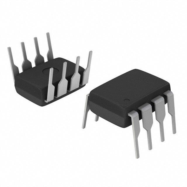
| 描述 | IC OPAMP AUDIO 8MHZ 8DIP音频放大器 SoundPlus(TM) Hi-Perf Aud Oper Amp |
| 产品分类 | Linear - Amplifiers - Instrumentation, OP Amps, Buffer Amps集成电路 - IC |
| 品牌 | Texas Instruments |
| 产品手册 | http://www.ti.com/litv/sbos058 |
| 产品图片 |
|
| rohs | 符合RoHS无铅 / 符合限制有害物质指令(RoHS)规范要求 |
| 产品系列 | 音频 IC,音频放大器,Texas Instruments OPA2134PASoundPlus™ |
| 数据手册 | |
| 产品型号 | OPA2134PA |
| THD+噪声 | 0.00015 % |
| 产品 | General Purpose Audio Amplifiers |
| 产品目录页面 | |
| 产品种类 | 音频放大器 |
| 供应商器件封装 | 8-PDIP |
| 共模抑制比—最小值 | 86 dB |
| 包装 | 管件 |
| 单位重量 | 528.600 mg |
| 压摆率 | 20 V/µs |
| 双重电源电压 | +/- 3 V, +/- 5 V, +/- 9 V |
| 商标 | Texas Instruments |
| 增益带宽生成 | 8 MHz |
| 增益带宽积 | 8MHz |
| 安装类型 | 通孔 |
| 安装风格 | Through Hole |
| 封装 | Tube |
| 封装/外壳 | 8-DIP(0.300",7.62mm) |
| 封装/箱体 | PDIP-8 |
| 工作温度 | -40°C ~ 85°C |
| 工作电源电压 | 5 V to 36 V |
| 工厂包装数量 | 50 |
| 放大器类型 | 音频 |
| 最大工作温度 | + 125 C |
| 最小工作温度 | - 40 C |
| 标准包装 | 50 |
| 电压-电源,单/双 (±) | 5 V ~ 36 V, ±2.5 V ~ 18 V |
| 电压-输入失调 | 500µV |
| 电流-电源 | 4mA |
| 电流-输入偏置 | 5pA |
| 电流-输出/通道 | 35mA |
| 电源电流 | 10 mA |
| 电源类型 | Dual |
| 电路数 | 2 |
| 类型 | 2-Channel FET Input |
| 系列 | OPA2134 |
| 设计资源 | http://www.digikey.com/product-highlights/cn/zh/texas-instruments-webench-design-center/3176 |
| 输入补偿电压 | 2 mV |
| 输出功率 | - |
| 输出类型 | - |


- 商务部:美国ITC正式对集成电路等产品启动337调查
- 曝三星4nm工艺存在良率问题 高通将骁龙8 Gen1或转产台积电
- 太阳诱电将投资9.5亿元在常州建新厂生产MLCC 预计2023年完工
- 英特尔发布欧洲新工厂建设计划 深化IDM 2.0 战略
- 台积电先进制程称霸业界 有大客户加持明年业绩稳了
- 达到5530亿美元!SIA预计今年全球半导体销售额将创下新高
- 英特尔拟将自动驾驶子公司Mobileye上市 估值或超500亿美元
- 三星加码芯片和SET,合并消费电子和移动部门,撤换高东真等 CEO
- 三星电子宣布重大人事变动 还合并消费电子和移动部门
- 海关总署:前11个月进口集成电路产品价值2.52万亿元 增长14.8%


PDF Datasheet 数据手册内容提取
Product Sample & Technical Tools & Support & Reference Folder Buy Documents Software Community Design OPA134,OPA2134,OPA4134 SBOS058A–DECEMBER1997–REVISEDOCTOBER2015 OPAx134 SoundPlus™ High Performance Audio Operational Amplifiers 1 Features 3 Description • SuperiorSoundQuality The OPA134 series are ultra-low distortion, low-noise 1 operational amplifiers fully specified for audio • UltraLowDistortion:0.00008% applications.AtrueFETinputstageisincorporatedto • LowNoise:8nV/√Hz provide superior sound quality and speed for • TrueFET-Input:I =5pA exceptional audio performance. This, in combination B with high output drive capability and excellent DC • HighSpeed: performance, allows for use in a wide variety of – SlewRate:20V/µs demanding applications. In addition, the OPA134 has – Bandwidth:8MHz a wide output swing, to within 1 V of the rails, allowing increased headroom and making it ideal for • HighOpen-LoopGain:120dB(600 Ω) useinanyaudiocircuit. • WideSupplyRange:±2.5Vto ±18V The OPA134 SoundPlus™ audio operational • Single,Dual,andQuadVersions amplifiers are easy to use and free from phase- inversion and the overload problems often found in 2 Applications common FET-input operational amplifiers. They can • ProfessionalAudioandMusic be operated from ±2.5-V to ±18-V power supplies. Input cascode circuitry provides excellent common- • LineDrivers mode rejection and maintains low input bias current • LineReceivers over its wide input voltage range, minimizing • MultimediaAudio distortion. OPA134 series operational amplifiers are • ActiveFilters unity-gain stable and provide excellent dynamic behavior over a wide range of load conditions, • Preamplifiers including high load capacitance. The dual and quad • Integrators versions feature completely independent circuitry for • CrossoverNetworks lowest crosstalk and freedom from interaction, even whenoverdrivenoroverloaded. THD+NoisevsFrequency Single and dual versions are available in 8-pin DIP 0.01 and SO-8 surface-mount packages in standard VO= 10Vrms configurations. The quad is available in 14-pin DIP R = 2kW L and SO-14 surface mount packages. All are specified for –40°C to 85°C operation. A SPICE macromodel is %) 0.001 e ( availablefordesignanalysis. s D+Noi VS= ±16 DeviceInformation(1) TH 0.0001 PARTNUMBER PACKAGE BODYSIZE(NOM) SOIC(8) 3.91mm×4.90mm OPA134 VS= ±17 VS= ±18 PDIP(8) 6.35mm×9.81mm 0.00001 20 100 1k 10k 20k SOIC(8) 3.91mm×4.90mm OPA2134 Frequency (Hz) PDIP(8) 6.35mm×9.81mm OPA4134 SOIC(14) 3.91mm×8.65mm (1) For all available packages, see the orderable addendum at theendofthedatasheet. 1 An IMPORTANT NOTICE at the end of this data sheet addresses availability, warranty, changes, use in safety-critical applications, intellectualpropertymattersandotherimportantdisclaimers.PRODUCTIONDATA.
OPA134,OPA2134,OPA4134 SBOS058A–DECEMBER1997–REVISEDOCTOBER2015 www.ti.com Table of Contents 1 Features.................................................................. 1 8 ApplicationandImplementation........................ 15 2 Applications........................................................... 1 8.1 ApplicationInformation............................................15 3 Description............................................................. 1 8.2 TypicalApplication .................................................16 4 RevisionHistory..................................................... 2 9 PowerSupplyRecommendations...................... 18 5 PinConfigurationandFunctions......................... 3 10 Layout................................................................... 18 6 Specifications......................................................... 4 10.1 LayoutGuidelines.................................................18 6.1 AbsoluteMaximumRatings......................................4 10.2 LayoutExample....................................................19 6.2 ESDRatings..............................................................4 11 DeviceandDocumentationSupport................. 20 6.3 RecommendedOperatingConditions.......................4 11.1 DeviceSupport ....................................................20 6.4 ElectricalCharacteristics...........................................5 11.2 DocumentationSupport .......................................20 6.5 TypicalCharacteristics..............................................7 11.3 RelatedLinks........................................................20 7 DetailedDescription............................................ 12 11.4 CommunityResources..........................................21 7.1 Overview.................................................................12 11.5 Trademarks...........................................................21 7.2 FunctionalBlockDiagram.......................................12 11.6 ElectrostaticDischargeCaution............................21 7.3 FeatureDescription.................................................12 11.7 Glossary................................................................21 7.4 DeviceFunctionalModes........................................14 12 Mechanical,Packaging,andOrderable Information........................................................... 21 4 Revision History NOTE:Pagenumbersforpreviousrevisionsmaydifferfrompagenumbersinthecurrentversion. ChangesfromOriginal(September2000)toRevisionA Page • AddedESDRatingstable,FeatureDescriptionsection,DeviceFunctionalModes,ApplicationandImplementation section,PowerSupplyRecommendationssection,Layoutsection,DeviceandDocumentationSupportsection,and Mechanical,Packaging,andOrderableInformationsection.................................................................................................. 1 2 SubmitDocumentationFeedback Copyright©1997–2015,TexasInstrumentsIncorporated ProductFolderLinks:OPA134 OPA2134 OPA4134
OPA134,OPA2134,OPA4134 www.ti.com SBOS058A–DECEMBER1997–REVISEDOCTOBER2015 5 Pin Configuration and Functions OPA134:PandDPackages 8-PinPDIPand8-PinSOIC OPA2134:PandDPackages TopView 8-PinPDIPand8-PinSOIC TopView OffsetTrim 1 8 OffsetTrim OutA 1 8 V+ –In 2 7 V+ A –InA 2 7 Out B +In 3 6 Output +InA 3 B 6 –In B V– 4 5 NC V– 4 5 +In B OPA4134:PandDPackages 14-PinPDIPand14-PinSOIC TopView OutA 1 14 Out D –InA 2 13 –In D A D +InA 3 12 +In D V+ 4 11 V– +In B 5 10 +In C B C –In B 6 9 –In C Out B 7 8 Out C PinFunctions:OPA134 PIN I/O DESCRIPTION NAME NO. OffsetTrim 1 I Inputoffsetvoltageadjust –In 2 I Invertinginput +In 3 I Noninvertinginput V– 4 — Negativepowersupply NC 5 — Nointernalconnection.Canbeleftfloating. Output 6 O Output V+ 7 — Positivepowersupply OffsetTrim 8 I Inputoffsetvoltageadjust PinFunctions:OPA2134andOPA4134 PIN OPA2134 OPA4134 I/O DESCRIPTION NAME NO. NO. OutA 1 1 O OutputchannelA –InA 2 2 I InvertinginputchannelA +InA 3 3 I NoninvertinginputchannelA V+ 8 4 — Positivepowersupply +InB 5 5 I NoninvertinginputchannelB –InB 6 6 I InvertinginputchannelB OutB 7 7 O OutputchannelB OutC — 8 O OutputchannelC –InC — 9 I InvertinginputchannelC +InC — 10 I NoninvertinginputchannelC Copyright©1997–2015,TexasInstrumentsIncorporated SubmitDocumentationFeedback 3 ProductFolderLinks:OPA134 OPA2134 OPA4134
OPA134,OPA2134,OPA4134 SBOS058A–DECEMBER1997–REVISEDOCTOBER2015 www.ti.com PinFunctions:OPA2134andOPA4134(continued) PIN OPA2134 OPA4134 I/O DESCRIPTION NAME NO. NO. V– 4 11 — Negativepowersupply +InD — 12 I NoninvertinginputchannelD –InD — 13 I InvertinginputchannelD OutD — 14 O OutputchannelD 6 Specifications 6.1 Absolute Maximum Ratings overoperatingfree-airtemperaturerange(unlessotherwisenoted) (1) MIN MAX UNIT Supplyvoltage,V+toV– 36 V Inputvoltage (V–)–0.7 (V+)+0.7 V Outputshortcircuit(2) Continuous Operatingtemperature –40 125 °C Junctiontemperature 150 °C Leadtemperature(soldering,10s) 300 °C T Storagetemperature –55 125 °C stg (1) StressesbeyondthoselistedunderAbsoluteMaximumRatingsmaycausepermanentdamagetothedevice.Thesearestressratings only,whichdonotimplyfunctionaloperationofthedeviceattheseoranyotherconditionsbeyondthoseindicatedunderRecommended OperatingConditions.Exposuretoabsolute-maximum-ratedconditionsforextendedperiodsmayaffectdevicereliability. (2) Short-circuittoground,oneamplifierperpackage. 6.2 ESD Ratings VALUE UNIT OPA134inPDIPandSOICPackage,OPA2134andOPA4134inPDIPPackage V Electrostaticdischarge Human-bodymodel(HBM),perANSI/ESDA/JEDECJS-001(1) ±2000 V (ESD) OPA2134inSOICPackage Human-bodymodel(HBM),perANSI/ESDA/JEDECJS-001(1) ±2000 V(ESD) Electrostaticdischarge Charged-devicemodel(CDM),perJEDECspecificationJESD22- V C101(2) ±500 OPA4134inSOICPackage Human-bodymodel(HBM),perANSI/ESDA/JEDECJS-001(1) ±2000 V(ESD) Electrostaticdischarge Charged-devicemodel(CDM),perJEDECspecificationJESD22- V C101(2) ±200 (1) JEDECdocumentJEP155statesthat500-VHBMallowssafemanufacturingwithastandardESDcontrolprocess. (2) JEDECdocumentJEP157statesthat250-VCDMallowssafemanufacturingwithastandardESDcontrolprocess. 6.3 Recommended Operating Conditions overoperatingfree-airtemperaturerange(unlessotherwisenoted) MIN NOM MAX UNIT VS Supplyvoltage,VS=(V+)–(V–) ±2.5 ±15 ±18 V T Specifiedtemperature –40 85 °C A 4 SubmitDocumentationFeedback Copyright©1997–2015,TexasInstrumentsIncorporated ProductFolderLinks:OPA134 OPA2134 OPA4134
OPA134,OPA2134,OPA4134 www.ti.com SBOS058A–DECEMBER1997–REVISEDOCTOBER2015 6.4 Electrical Characteristics AtT =+25°C,V =±15V,unlessotherwisenoted A S PARAMETER TESTCONDITIONS MIN TYP MAX UNIT AUDIOPERFORMANCE TotalHarmonicDistortion+Noise G=1,f=1kHz,VO=3 RL=2kΩ 0.00008% Vrms R =600Ω 0.00015% L IntermodulationDistortion G=1,f=1kHz,V =1Vp-p –98 dB O Headroom(1) THD<0.01%,R =2kΩ,V =18V 23.6 dBu L S FREQUENCYRESPONSE Gain-BandwidthProduct 8 MHz SlewRate(2) ±15 ±20 V/µs FullPowerBandwidth 1.3 MHz SettlingTime0.1% G=1,10-VStep,C =100pF 0.7 µs L SettlingTime0.01% G=1,10-VStep,C =100pF 1 µs L OverloadRecoveryTime (V )×(Gain)=V 0.5 µs IN S NOISE NoiseVoltage, 1.2 µVrms InputVoltage f=20Hzto20kHz Noise NoiseDensity, 8 nV/√Hz f=1kHz CurrentNoiseDensity,f=1kHz 3 fA/√Hz OFFSETVOLTAGE ±0.5 ±2 InputOffsetVoltage mV T =–40°Cto85°C ±1 ±3(3) A InputOffsetVoltagevsTemperature T =–40°Cto85°C ±2 µV/°C A InputOffsetVoltagevsPowerSupply V =±2.5Vto±18V 90 106 dB (PSRR) S DC,R =2kΩ 135 L ChannelSeperation(Dual,Quad) dB f=20kHz,R =2kΩ 130 L INPUTBIASCURRENT InputBiasCurrent(4) V =0V 5 ±100 pA CM InputBiasCurrentvsTemperature(3) SeeTypical ±5 nA Characteristics InputOffsetCurrent(4) V =0V ±2 ±50 pA CM INPUTVOLTAGERANGE Common-ModeVoltageRange (V–)+2.5 13 (V+)–2.5 V V =–12.5Vto12.5V 86 100 CM Common-ModeRejection dB T =–40°Cto85°C 90 A INPUTIMPEDANCE Differential 1013||2 Ω||pF Common-Mode V =–12.5Vto12.5V 1013||5 Ω||pF CM OPEN-LOOPGAIN R =10kΩ,V =–14.5Vto13.8V 104 120 L O Open-LoopVoltageGain R =2kΩ,V =–13.8Vto13.5V 104 120 dB L O R =600Ω,V =–12.8Vto12.5V 104 120 L O (1) dBu=20*log(Vrms/0.7746)whereVrmsisthemaximumoutputvoltageforwhichTHD+Noiseislessthan0.01%.SeeTHD+Noisetext. (2) Proposedbydesign. (3) Proposedbywafer-leveltestto95%confidencelevel. (4) High-speedtestatT =25°C. J Copyright©1997–2015,TexasInstrumentsIncorporated SubmitDocumentationFeedback 5 ProductFolderLinks:OPA134 OPA2134 OPA4134
OPA134,OPA2134,OPA4134 SBOS058A–DECEMBER1997–REVISEDOCTOBER2015 www.ti.com Electrical Characteristics (continued) AtT =+25°C,V =±15V,unlessotherwisenoted A S PARAMETER TESTCONDITIONS MIN TYP MAX UNIT OUTPUT R =10kΩ (V–)+0.5 (V+)–1.2 L VoltageOutput R =2kΩ (V–)+1.2 (V+)–1.5 V L R =600Ω (V–)+2.2 (V+)–2.5 L OutputCurrent ±35 mA OutputImpedance,Closed-Loop(5) f=10kHz 0.01 Ω OutputImpedance,Open-Loop f=10kHz 10 Ω Short-CircuitCurrent ±40 mA CapacitiveLeadDrive(Stable SeeTypical Operation) Characteristics POWERSUPPLY SpecifiedOperatingVoltage ±15 V OperatingVoltageRange ±2.5 ±18 V QuiescentCurrent(peramplifier) I =0 4 5 mA O TEMPERATURERANGE SpecifiedRange –40 85 °C OperatingRange –55 125 °C (5) SeeFigure14 6 SubmitDocumentationFeedback Copyright©1997–2015,TexasInstrumentsIncorporated ProductFolderLinks:OPA134 OPA2134 OPA4134
OPA134,OPA2134,OPA4134 www.ti.com SBOS058A–DECEMBER1997–REVISEDOCTOBER2015 6.5 Typical Characteristics AtT =25°C,V =15V,R =2kΩ,unlessotherwisenoted. A S L 0.1 5 R G = +1 26Lk0W0W 1 fR =L =1k 2HkzW 0.01 %) se ( %) 0.1 Noi 0.001 D ( OPA134 D+ G = +10 IM OP176 H 0.010 T OPA134 0.0001 G = +1 Baseline VO= 3Vrms 0.001 0.00001 0.0005 10 100 1k 10k 100k 30m 0.1 1 10 30 Frequency (Hz) OutputAmplitude (Vpp) Figure1.TotalHarmonicDistortion+NoisevsFrequency Figure2.SMPTEIntermodulationDistortionvsOutput Amplitude 0.01 1 RVOL== 21k0WVrms VfR =SL =1=k 2±Hk1zW8V TOOHPPDA171 <63 40–.–01111%.11.V7Vrmrmss 0.1 %) 0.001 %) THD+Noise ( 0.0001 VS= ±16 THD+Noise ( 0.010 OPA134 OP176 OPA134 VS= ±17 VS= ±18 0.001 Baseline 0.00001 0.0005 20 100 1k 10k 20k 0.1 1 10 20 Frequency (Hz) OutputAmplitude (Vrms) Figure3.TotalHarmonicDistortion+NoisevsFrequency Figure4.Headroom–TotalHarmonicDistortion+Noisevs OutputAmplitude 0.01 1k 2nd Harmonic s) 3rd Harmonic OP176+ ntal 0.001 z) 100 Resistor e H m Ö nda = 600W nV/ plitude (% of Fu 00.0.00000011 RRL L = 2kW Voltage Noise ( 101 ORPeAs1is3to4r+ Am VO= 1Vrms ResisOtonrl yNoise Vn(total) = Ö(niRS)2+ en2+ 4kTRS 0.000001 0.1 20 100 1k 10k 20k 10 100 1k 10k 100k 1M 10M Frequency (Hz) Source Resistance (W) Figure5.HarmonicDistortion+NoisevsFrequency Figure6.VoltageNoisevsSourceResistance Copyright©1997–2015,TexasInstrumentsIncorporated SubmitDocumentationFeedback 7 ProductFolderLinks:OPA134 OPA2134 OPA4134
OPA134,OPA2134,OPA4134 SBOS058A–DECEMBER1997–REVISEDOCTOBER2015 www.ti.com Typical Characteristics (continued) AtT =25°C,V =15V,R =2kΩ,unlessotherwisenoted. A S L 1k 100 R = 20W S Noise (nV/ÖHz) Noise (fA/ÖHz) 100 Voltage Noise Voltage (mV) 10 Peak-to-Peak Voltage Current 10 Noise 1 RMS Current Noise 1 0.1 1 10 100 1k 10k 100k 1M 1 10 100 1k 10k 100k Frequency(Hz) Noise Bandwidth (Hz) Figure7.InputVoltageandCurrentNoiseSpectralDensity Figure8.Input-ReferredNoiseVoltagevsNoiseBandwidth vsFrequency 160 0 50 140 40 Voltage Gain (dB) 11208642000000 G f –––4915035 PhaseShift (°) Closed-Loop Gain (dB) 3210000 GGG == = ++ +110100 –10 0 –180 –20 –20 0.1 1 10 100 1k 10k 100k 1M 10M 1k 10k 100k 1M 10M Frequency (Hz) Frequency (Hz) Figure9.Open-LoopGainandPhasevsFrequency Figure10.Closed-LoopGainvsFrequency 120 160 R =∞ L 100 –PSR B) 140 d R (dB) 80 ation ( PSR, CM 6400 +PSR nnel Separ 120 DGQu u=aa ld1 a ,m n adel laq csuhuaarden dnd eeclvhsia.cnens.el RL= 2kW ha 100 Ato D or B to C—other 20 CMR C combinations yield improved rejection. 0 80 10 100 1k 10k 100k 1M 100 1k 10k 100k Frequency (Hz) Frequency (Hz) Figure11.PowerSupplyandCommon-ModeRejectionvs Figure12.ChannelSeparationvsFrequency Frequency 8 SubmitDocumentationFeedback Copyright©1997–2015,TexasInstrumentsIncorporated ProductFolderLinks:OPA134 OPA2134 OPA4134
OPA134,OPA2134,OPA4134 www.ti.com SBOS058A–DECEMBER1997–REVISEDOCTOBER2015 Typical Characteristics (continued) AtT =25°C,V =15V,R =2kΩ,unlessotherwisenoted. A S L 30 10 Maximum output voltage Note: Open-Loop VS= ±15V iwndituhcoeudt sdleiswto-rrtaioten Wce () 1 Oatu ft p=u 1t 0ImkHpze disa n1c0eW p) an Output Voltage (Vp- 2100 VS= ±5V ed-Loop Output Imped 00.00.00.111 GGG === +++112000 s o VS= ±2.5V Cl G = +1 0 0.0001 10k 100k 1M 10M 10 100 1k 10k 100k Frequency (Hz) Frequency (Hz) Figure13.MaximumOutputVoltagevsFrequency Figure14.Closed-LoopOutputImpedancevsFrequency 100k 10 High SpeedTest 9 High SpeedTest Warmed Up 10k 8 A) A) Current (p 1010k Current (p 765 Input Bias 10 Dual Input Bias 432 1 Single 1 0.1 0 –75 –50 –25 0 25 50 75 100 125 –15 –10 –5 0 5 10 15 AmbientTemperature (°C) Common-Mode Voltage (V) Figure15.InputBiasCurrentvsTemperature Figure16.InputBiasCurrentvsInputCommon-Mode Voltage 150 120 R = 600W L 140 B) RL= 2kW p Gain (d 130 PSR (dB) 110 PSR Open-Loo 120 RL= 10kW CMR, 100 110 CMR 100 90 –75 –50 –25 0 25 50 75 100 125 –75 –50 –25 0 25 50 75 100 125 Temperature (°C) AmbientTemperature (°C) Figure17.Open-LoopGainvsTemperature Figure18.CMR,PSRvsTemperature Copyright©1997–2015,TexasInstrumentsIncorporated SubmitDocumentationFeedback 9 ProductFolderLinks:OPA134 OPA2134 OPA4134
OPA134,OPA2134,OPA4134 SBOS058A–DECEMBER1997–REVISEDOCTOBER2015 www.ti.com Typical Characteristics (continued) AtT =25°C,V =15V,R =2kΩ,unlessotherwisenoted. A S L 4.3 60 15 V = 15V 14 IN uiescent Current PerAmp (mA) 4443....2109 ±IQ ±ISC 54320000 Short-Circuit Current (mA) Output Voltage Swing (V) ––––1111111111320023 1251°C258°5C°C 85°C–2555°°2CC255°C°C–55°C Q –14 V =–15V 3.8 10 –15 IN –75 –50 –25 0 25 50 75 100 125 0 10 20 30 40 50 60 AmbientTemperature (°C) Output Current (mA) Figure19.QuiescentCurrentandShort-CircuitCurrentvs Figure20.OutputVoltageSwingvsOutputCurrent Temperature 18 12 Typical production Typical production 16 distribution of packaged distribution of packaged 10 %) 14 units. %) units. s ( 12 s ( 8 er er plifi 10 plifi m m 6 A 8 A of of nt 6 nt 4 e e erc 4 erc P P 2 2 0 0 200018001600140012001000–800–600–400–2000200400600800100012001400160018002000 0.5 1.5 2.5 3.5 4.5 5.5 6.5 7.5 8.5 9.5 10.5 11.5 12.5 –––––– Offset Voltage (V) Offset Voltage Drift (µV/°C) Figure21.OffsetVoltageProductionDistribution Figure22.OffsetVoltageDriftProductionDistribution v di v V/ di m V/ 0 5 5 200ns/div 1μs/div Figure23.Small-SignalStepResponseG=1,CL=100pF Figure24.Large-SignalStepResponseG=1,CL=100pF 10 SubmitDocumentationFeedback Copyright©1997–2015,TexasInstrumentsIncorporated ProductFolderLinks:OPA134 OPA2134 OPA4134
OPA134,OPA2134,OPA4134 www.ti.com SBOS058A–DECEMBER1997–REVISEDOCTOBER2015 Typical Characteristics (continued) AtT =25°C,V =15V,R =2kΩ,unlessotherwisenoted. A S L 100 60 50 G = +1 µs) 10 0.01% %) 40 G =–1 me ( ot ( Ti ho 30 ettling 1 0.1% Overs 20 S 10 G = ±10 0.1 0 ±1 ±10 ±100 ±1000 100pF 1nF 10nF Closed-Loop Gain (V/V) Load Capacitance Figure25.SettlingTimevsClosed-LoopGain Figure26.Small-SignalOvershootvsLoadCapacitance Copyright©1997–2015,TexasInstrumentsIncorporated SubmitDocumentationFeedback 11 ProductFolderLinks:OPA134 OPA2134 OPA4134
OPA134,OPA2134,OPA4134 SBOS058A–DECEMBER1997–REVISEDOCTOBER2015 www.ti.com 7 Detailed Description 7.1 Overview The OPA134 series are ultra-low distortion, low-noise operational amplifiers fully specified for audio applications. A true FET input stage is incorporated to provide superior sound quality and speed for exceptional audio performance. This, in combination with high output drive capability and excellent DC performance, allows for use in a wide variety of demanding applications. In addition, the OPA134 has a wide output swing, to within 1 V of therails,allowingincreasedheadroomandmakingitidealforuseinanyaudiocircuit. 7.2 Functional Block Diagram Input Offset Adjust (OPA134 only) +IN + Output -IN – Input Offset Compensation Adjust (OPA134 only) 7.3 Feature Description 7.3.1 TotalHarmonicDistortion The OPA134 series of operational amplifiers have excellent distortion characteristics. THD+Noise is below 0.0004%throughouttheaudiofrequencyrange,20Hzto20kHz,witha2-kΩ load.Inaddition,distortionremains relatively flat through its wide output voltage swing range, providing increased headroom compared to other audioamplifiers,includingtheOP176/275. Headroom is a subjective measurement, and can be thought of as the maximum output amplitude allowed while still maintaining a low level of distortion. In an attempt to quantify headroom, TI defines very low distortion as 0.01%. Headroom is expressed as a ratio which compares the maximum allowable output voltage level to a standard output level (1 mW into 600 Ω, or 0.7746 Vrms). Therefore, OPA134 series of operational amplifiers, which have a maximum allowable output voltage level of 11.7 Vrms (THD+Noise < 0.01%), have a headroom specificationof23.6dBu.SeeFigure4. 7.3.2 DistortionMeasurements The distortion produced by OPA134 series of operational amplifiers is below the measurement limit of all known commercially-availableequipment.However,aspecialtestcircuitcanextendthemeasurementcapabilities. Operational amplifier distortion can be considered an internal error source which can be referred to the input. Figure 27 shows a circuit which causes the operational amplifier distortion to be 101 times greater than that which the operational amplifier normally produces. The addition of R3 to the otherwise standard non-inverting amplifier configuration alters the feedback factor or noise gain of the circuit. The closed-loop gain is unchanged, butthefeedbackavailableforerrorcorrectionisreducedbyafactorof101,thusextendingtheresolutionby101. Theinputsignalandloadappliedtotheoperationalamplifierarethesameaswithconventionalfeedbackwithout R3.ThevalueofR3shouldbekeptsmalltominimizeitseffectonthedistortionmeasurements. 12 SubmitDocumentationFeedback Copyright©1997–2015,TexasInstrumentsIncorporated ProductFolderLinks:OPA134 OPA2134 OPA4134
OPA134,OPA2134,OPA4134 www.ti.com SBOS058A–DECEMBER1997–REVISEDOCTOBER2015 Feature Description (continued) R R 1 2 SIG. DIST. GAIN GAIN R1 R2 R3 1 101 ∞ 1kW 10W 11 101 100W 1kW 11W R R3 OPA134 VO= 3Vrms 101 101 10W 1kW ∞ Signal Gain = 1+ 2 R 1 R Distortion Gain = 1+ 2 R II R 1 3 Generator Analyzer Output Input Audio Precision IBM PC R System One 1kWL or Analyzer(1) Compatible NOTE: (1) Measurement BW = 80kHz Figure27. DistortionTestCircuit This technique can be verified by duplicating measurements at high gain or high frequency, where the distortion is within the measurement capability of the test equipment. Measurements for this data sheet were made with an Audio Precision distortion and noise analyzer, which greatly simplifies repetitive measurements. The measurementtechniquecan,however,beperformedwithmanualdistortionmeasurementinstruments. 7.3.3 SourceImpedanceandDistortion For lowest distortion with a source or feedback network with an impedance greater than 2 kΩ, the impedance seenbythepositiveandnegativeinputsinnoninvertingapplicationsshouldbematched.Thep-channelJFETsin the FET input stage exhibit a varying input capacitance with applied common-mode input voltage. In inverting configurations, the input does not vary with input voltage, because the inverting input is held at virtual ground. However, in noninverting applications the inputs do vary, and the gate-to-source voltage is not constant. The effect is increased distortion due to the varying capacitance for unmatched source impedances greater than 2 kΩ. To maintain low distortion, match unbalanced source impedance with the appropriate values in the feedback network as shown in Figure 28. Of course, the unbalanced impedance may be from gain-setting resistors in the feedback path. If the parallel combination of R1 and R2 is greater than 2 kΩ, use a matching impedance on the noninvertinginput.Asalways,minimizeresistorvaluestoreducetheeffectsofthermalnoise. R R 1 2 OPA134 VOUT V IN If R > 2kW or R II R > 2kW S 1 2 R = R II R S 1 2 Figure28. ImpedanceMatchingforMaintainingLowDistortioninNon-InvertingCircuits 7.3.4 PhaseReversalProtection The OPA134 series of operational amplifiers are free from output phase-reversal problems. Many audio operational amplifiers, such as the OP176, exhibit phase-reversal of the output when the input common-mode voltage range is exceeded. This can occur in voltage-follower circuits, causing serious problems in control loop applications. The OPA134 series operational amplifiers are free from this undesirable behavior even with inputs of10-Vbeyondtheinputcommon-moderange. Copyright©1997–2015,TexasInstrumentsIncorporated SubmitDocumentationFeedback 13 ProductFolderLinks:OPA134 OPA2134 OPA4134
OPA134,OPA2134,OPA4134 SBOS058A–DECEMBER1997–REVISEDOCTOBER2015 www.ti.com Feature Description (continued) 7.3.5 OutputCurrentLimit Output current is limited by internal circuitry to approximately ±40 mA at 25°C. The limit current decreases with increasingtemperature,asshowninFigure19. 7.4 Device Functional Modes 7.4.1 NoisePerformance Circuit noise is determined by the thermal noise of external resistors and operational amplifier noise. Operational amplifier noise is described by two parameters: noise voltage and noise current. The total noise is quantified by theequation: V (total)= (i R )2e 2 +4kTR n n S n S (1) With low source impedance, the current noise term is insignificant and voltage noise dominates the noise performance.Athighsourceimpedance,thecurrentnoisetermbecomesthedominantcontributor. Low-noise bipolar operational amplifiers such as the OPA27 and OPA37 provide low voltage noise at the expense of a higher current noise. However, OPA134 series operational amplifiers provide both low voltage noise and low current noise. This provides optimum noise performance over a wide range of sources, including reactive source impedances; refer to Figure 6. Above 2-kΩ source resistance, the operational amplifier contributes little additional noise; the voltage and current terms in the total noise equation become insignificant and the source resistance term dominates. Below 2 kΩ, operational amplifier voltage noise dominates over the resistornoise,butcomparesfavorablywithotheraudiooperationalamplifierssuchastheOP176. 14 SubmitDocumentationFeedback Copyright©1997–2015,TexasInstrumentsIncorporated ProductFolderLinks:OPA134 OPA2134 OPA4134
OPA134,OPA2134,OPA4134 www.ti.com SBOS058A–DECEMBER1997–REVISEDOCTOBER2015 8 Application and Implementation NOTE Information in the following applications sections is not part of the TI component specification, and TI does not warrant its accuracy or completeness. TI’s customers are responsible for determining suitability of components for their purposes. Customers should validateandtesttheirdesignimplementationtoconfirmsystemfunctionality. 8.1 Application Information The OPA134 series operational amplifiers are unity-gain stable, and suitable for a wide range of audio and general-purpose applications. All circuitry is independent in the dual version, assuring normal behavior when one amplifierinapackageisoverdrivenorshort-circuited.Powersupplypinsshouldbebypassedwith10-nFceramic capacitorsorlargertominimizepowersupplynoise. 8.1.1 OperatingVoltage The OPA134 series of operational amplifiers operate with power supplies from ±2.5 V to ±18 V with excellent performance. Although specifications are production tested with ±15-V supplies, most behavior remains unchanged throughout the full operating voltage range. Parameters which vary significantly with operating voltageareshowninTypicalCharacteristics. 8.1.2 OffsetVoltageTrim Offset voltage of OPA134 series amplifiers is laser-trimmed, and usually requires no user adjustment. The OPA134 (single operational amplifier version) provides offset trim connections on pins 1 and 8, identical to 5534 amplifiers. Offset voltage can be adjusted by connecting a potentiometer as shown in Figure 29. This adjustment should be used only to null the offset of the operational amplifier, not to adjust system offset or offset produced by the signal source. Nulling offset could change the offset voltage drift behavior of the operational amplifier. Whileitisnotpossibletopredicttheexactchangeindrift,theeffectisusuallysmall. V+ Trim Range: ±4mV typ 10nF 100kW 7 2 1 8 OPA134 3 6 4 OPA134 single op amp only. 10nF Use offset adjust pins only to null offset voltage of op amp—see text. V– Figure29. OPA134OffsetVoltageTrimCircuit Copyright©1997–2015,TexasInstrumentsIncorporated SubmitDocumentationFeedback 15 ProductFolderLinks:OPA134 OPA2134 OPA4134
OPA134,OPA2134,OPA4134 SBOS058A–DECEMBER1997–REVISEDOCTOBER2015 www.ti.com 8.2 Typical Application The OPAx134 family offers outstanding dc precision and AC performance. These devices operate up to 36-V supply rails and offer ultralow distortion and noise, as well as 8-MHz bandwidth and high capacitive load drive. ThesefeaturesmaketheOPAx134arobust,high-performanceoperationalamplifierforhigh-voltageprofessional audioapplications. 2.94 k(cid:13) 1 nF 590 (cid:13) 499 (cid:13) Input – Output 39 nF + Figure30. OPA1342ndOrder30-kHz,LowPassFilterSchematic 8.2.1 DesignRequirements • Gain=5V/V(inverting) • Lowpasscutofffrequency=30kHz • –40db/decfilterresponse • Maintainlessthan3-dBgainpeakinginthegainversusfrequencyresponse 8.2.2 DetailedDesignProcedure The infinite-gain multiple-feedback circuit for a low-pass network function is shown in Figure 30. The voltage transferfunctionis: Output (cid:16)1RR C C (cid:11)s(cid:12) 1 3 2 5 Input s2(cid:14)(cid:11)s C (cid:12)(cid:11)1R (cid:14)1R (cid:14)1R (cid:12)(cid:14)1R R C C 2 1 3 4 3 4 2 5 (2) This circuit produces a signal inversion. For this circuit the gain at DC and the low pass cutoff frequency are calculatedusingEquation3. R Gain 4 R 1 1 f (cid:11)1R R C C (cid:12) C 3 4 2 5 2S (3) Software tools are readily available to simplify filter design. WEBENCH® Filter Designer is a simple, powerful, and easy-to-use active filter design program. The WEBENCH Filter Designer lets you create optimized filter designsusingaselectionofTIoperationalamplifiersandpassivecomponentsfromTI'svendorpartners. Available as a web based tool from the WEBENCH® Design Center, WEBENCH® Filter Designer allows you to design,optimize,andsimulatecompletemultistageactivefiltersolutionswithinminutes. 16 SubmitDocumentationFeedback Copyright©1997–2015,TexasInstrumentsIncorporated ProductFolderLinks:OPA134 OPA2134 OPA4134
OPA134,OPA2134,OPA4134 www.ti.com SBOS058A–DECEMBER1997–REVISEDOCTOBER2015 Typical Application (continued) 8.2.3 ApplicationCurve 20 0 b) d n ( -20 ai G -40 -60 100 1k 10k 100k 1M Frequency (Hz) Figure31. OPA1342ndOrder30-kHz,LowPassFilterResponse Copyright©1997–2015,TexasInstrumentsIncorporated SubmitDocumentationFeedback 17 ProductFolderLinks:OPA134 OPA2134 OPA4134
OPA134,OPA2134,OPA4134 SBOS058A–DECEMBER1997–REVISEDOCTOBER2015 www.ti.com 9 Power Supply Recommendations The OPAx134 is specified for operation from 5 V to 36 V (±2.5 V to ±18 V); many specifications apply from –40°C to 85°C. Parameters that can exhibit significant variance with regard to operating voltage or temperature arepresentedintheTypicalCharacteristics. CAUTION Supply voltages larger than 36 V can permanently damage the device; see the AbsoluteMaximumRatings. Place 10-nF bypass capacitors close to the power-supply pins to reduce errors coupling in from noisy or high- impedance power supplies. For more detailed information on bypass capacitor placement, see the Layout Guidelines. 10 Layout 10.1 Layout Guidelines Forbestoperationalperformanceofthedevice,usegoodPCBlayoutpractices,including: • Noise can propagate into analog circuitry through the power pins of the circuit as a whole and operational amplifier itself. Bypass capacitors are used to reduce the coupled noise by providing low-impedance power sourceslocaltotheanalogcircuitry. – Connect low-ESR, 10-nF ceramic bypass capacitors between each supply pin and ground, placed as close to the device as possible. A single bypass capacitor from V+ to ground is applicable for single- supplyapplications. • Separate grounding for analog and digital portions of circuitry is one of the simplest and most-effective methods of noise suppression. One or more layers on multilayer PCBs are usually devoted to ground planes. A ground plane helps distribute heat and reduces EMI noise pickup. Make sure to physically separate digital and analog grounds paying attention to the flow of the ground current. For more detailed information refer to CircuitBoardLayoutTechniques,SLOA089. • In order to reduce parasitic coupling, run the input traces as far away from the supply or output traces as possible. If these traces cannot be kept separate, crossing the sensitive trace perpendicular is much better as opposedtoinparallelwiththenoisytrace. • Place the external components as close to the device as possible. As shown in Layout Example, keeping RF andRGclosetotheinvertinginputminimizesparasiticcapacitance. • Keep the length of input traces as short as possible. Always remember that the input traces are the most sensitivepartofthecircuit. • Consider a driven, low-impedance guard ring around the critical traces. A guard ring can significantly reduce leakagecurrentsfromnearbytracesthatareatdifferentpotentials. • CleaningthePCBfollowingboardassemblyisrecommendedforbestperformance. • Any precision integrated circuit may experience performance shifts due to moisture ingress into the plastic package. Following any aqueous PCB cleaning process, baking the PCB assembly is recommended to remove moisture introduced into the device packaging during the cleaning process. A low temperature, post cleaningbakeat85°Cfor30minutesissufficientformostcircumstances. 18 SubmitDocumentationFeedback Copyright©1997–2015,TexasInstrumentsIncorporated ProductFolderLinks:OPA134 OPA2134 OPA4134
OPA134,OPA2134,OPA4134 www.ti.com SBOS058A–DECEMBER1997–REVISEDOCTOBER2015 10.2 Layout Example VIN + RG VOUT RF (Schematic Representation) Place components Run the input traces close to device and to as far away from each other to reduce the supply lines parasitic errors VS+ RF as possible Offset trim Offset trim RG GND –IN V+ GND VIN +IN OUTPUT V– NC Use low-ESR, ceramic bypass capacitor Use low-ESR, GND VS– VOUT ceramic bypass Ground (GND) plane on another layer capacitor Figure32. OPA134LayoutExamplefortheNoninvertingConfiguration Copyright©1997–2015,TexasInstrumentsIncorporated SubmitDocumentationFeedback 19 ProductFolderLinks:OPA134 OPA2134 OPA4134
OPA134,OPA2134,OPA4134 SBOS058A–DECEMBER1997–REVISEDOCTOBER2015 www.ti.com 11 Device and Documentation Support 11.1 Device Support 11.1.1 DevelopmentSupport 11.1.1.1 WEBENCHFilterDesignerTool WEBENCH® Filter Designer is a simple, powerful, and easy-to-use active filter design program. The WEBENCH Filter Designer lets you create optimized filter designs using a selection of TI operational amplifiers and passive componentsfromTI'svendorpartners. 11.1.1.2 TINA-TI™(FreeSoftwareDownload) TINA™ is a simple, powerful, and easy-to-use circuit simulation program based on a SPICE engine. TINA-TI is a free, fully-functional version of the TINA software, preloaded with a library of macro models in addition to a range of both passive and active models. TINA-TI provides all the conventional dc, transient, and frequency domain analysisofSPICE,aswellasadditionaldesigncapabilities. Available as a free download from the Analog eLab Design Center, TINA-TI offers extensive post-processing capability that allows users to format results in a variety of ways. Virtual instruments offer the ability to select inputwaveformsandprobecircuitnodes,voltages,andwaveforms,creatingadynamicquick-starttool. NOTE These files require that either the TINA software (from DesignSoft™) or TINA-TI software beinstalled.DownloadthefreeTINA-TIsoftwarefromtheTINA-TIfolder. 11.1.1.3 TIPrecisionDesigns TheOPAx134isfeaturedinseveralTIPrecisionDesigns,availableonlineat http://www.ti.com/ww/en/analog/precision-designs/. TI Precision Designs are analog solutions created by TI’s precision analog applications experts and offer the theory of operation, component selection, simulation, completePCBschematicandlayout,billofmaterials,andmeasuredperformanceofmanyusefulcircuits. 11.2 Documentation Support 11.2.1 RelatedDocumentation Forrelateddocumentation,seethefollowing: • EMIRejectionRatioofOperationalAmplifiers,SBOA128 • CircuitBoardLayoutTechniques,SLOA089 11.3 Related Links The table below lists quick access links. Categories include technical documents, support and community resources,toolsandsoftware,andquickaccesstosampleorbuy. Table1.RelatedLinks TECHNICAL TOOLS& SUPPORT& PARTS PRODUCTFOLDER SAMPLE&BUY DOCUMENTS SOFTWARE COMMUNITY OPA134 Clickhere Clickhere Clickhere Clickhere Clickhere OPA2134 Clickhere Clickhere Clickhere Clickhere Clickhere OPA4134 Clickhere Clickhere Clickhere Clickhere Clickhere 20 SubmitDocumentationFeedback Copyright©1997–2015,TexasInstrumentsIncorporated ProductFolderLinks:OPA134 OPA2134 OPA4134
OPA134,OPA2134,OPA4134 www.ti.com SBOS058A–DECEMBER1997–REVISEDOCTOBER2015 11.4 Community Resources The following links connect to TI community resources. Linked contents are provided "AS IS" by the respective contributors. They do not constitute TI specifications and do not necessarily reflect TI's views; see TI's Terms of Use. TIE2E™OnlineCommunity TI'sEngineer-to-Engineer(E2E)Community.Createdtofostercollaboration amongengineers.Ate2e.ti.com,youcanaskquestions,shareknowledge,exploreideasandhelp solveproblemswithfellowengineers. DesignSupport TI'sDesignSupport QuicklyfindhelpfulE2Eforumsalongwithdesignsupporttoolsand contactinformationfortechnicalsupport. 11.5 Trademarks SoundPlus,TINA-TI,E2EaretrademarksofTexasInstruments. TINA,DesignSoftaretrademarksofDesignSoft,Inc. Allothertrademarksarethepropertyoftheirrespectiveowners. 11.6 Electrostatic Discharge Caution Thesedeviceshavelimitedbuilt-inESDprotection.Theleadsshouldbeshortedtogetherorthedeviceplacedinconductivefoam duringstorageorhandlingtopreventelectrostaticdamagetotheMOSgates. 11.7 Glossary SLYZ022—TIGlossary. Thisglossarylistsandexplainsterms,acronyms,anddefinitions. 12 Mechanical, Packaging, and Orderable Information The following pages include mechanical, packaging, and orderable information. This information is the most current data available for the designated devices. This data is subject to change without notice and revision of thisdocument.Forbrowser-basedversionsofthisdatasheet,refertotheleft-handnavigation. Copyright©1997–2015,TexasInstrumentsIncorporated SubmitDocumentationFeedback 21 ProductFolderLinks:OPA134 OPA2134 OPA4134
PACKAGE OPTION ADDENDUM www.ti.com 6-Feb-2020 PACKAGING INFORMATION Orderable Device Status Package Type Package Pins Package Eco Plan Lead/Ball Finish MSL Peak Temp Op Temp (°C) Device Marking Samples (1) Drawing Qty (2) (6) (3) (4/5) OPA134PA ACTIVE PDIP P 8 50 Green (RoHS NIPDAU N / A for Pkg Type OPA134PA & no Sb/Br) OPA134PAG4 ACTIVE PDIP P 8 50 Green (RoHS NIPDAU N / A for Pkg Type OPA134PA & no Sb/Br) OPA134UA ACTIVE SOIC D 8 75 Green (RoHS NIPDAU Level-3-260C-168 HR -40 to 85 OPA & no Sb/Br) 134UA OPA134UA/2K5 ACTIVE SOIC D 8 2500 Green (RoHS NIPDAU Level-3-260C-168 HR -40 to 85 OPA & no Sb/Br) 134UA OPA134UAE4 ACTIVE SOIC D 8 75 Green (RoHS NIPDAU Level-3-260C-168 HR -40 to 85 OPA & no Sb/Br) 134UA OPA134UAG4 ACTIVE SOIC D 8 75 Green (RoHS NIPDAU Level-3-260C-168 HR -40 to 85 OPA & no Sb/Br) 134UA OPA2134PA ACTIVE PDIP P 8 50 Green (RoHS NIPDAU N / A for Pkg Type -40 to 85 OPA2134PA & no Sb/Br) OPA2134PAG4 ACTIVE PDIP P 8 50 Green (RoHS NIPDAU N / A for Pkg Type -40 to 85 OPA2134PA & no Sb/Br) OPA2134UA ACTIVE SOIC D 8 75 Green (RoHS NIPDAU Level-3-260C-168 HR -40 to 85 OPA & no Sb/Br) 2134UA OPA2134UA/2K5 ACTIVE SOIC D 8 2500 Green (RoHS NIPDAU Level-3-260C-168 HR -40 to 85 OPA & no Sb/Br) 2134UA OPA2134UA/2K5E4 ACTIVE SOIC D 8 2500 Green (RoHS NIPDAU Level-3-260C-168 HR -40 to 85 OPA & no Sb/Br) 2134UA OPA2134UAE4 ACTIVE SOIC D 8 75 Green (RoHS NIPDAU Level-3-260C-168 HR -40 to 85 OPA & no Sb/Br) 2134UA OPA2134UAG4 ACTIVE SOIC D 8 75 Green (RoHS NIPDAU Level-3-260C-168 HR -40 to 85 OPA & no Sb/Br) 2134UA OPA4134UA ACTIVE SOIC D 14 50 Green (RoHS NIPDAU Level-3-260C-168 HR -40 to 85 OPA4134UA & no Sb/Br) OPA4134UA/2K5 ACTIVE SOIC D 14 2500 Green (RoHS NIPDAU Level-3-260C-168 HR -40 to 85 OPA4134UA & no Sb/Br) OPA4134UA/2K5E4 ACTIVE SOIC D 14 2500 Green (RoHS NIPDAU Level-3-260C-168 HR -40 to 85 OPA4134UA & no Sb/Br) OPA4134UAE4 ACTIVE SOIC D 14 50 Green (RoHS NIPDAU Level-3-260C-168 HR -40 to 85 OPA4134UA & no Sb/Br) Addendum-Page 1
PACKAGE OPTION ADDENDUM www.ti.com 6-Feb-2020 Orderable Device Status Package Type Package Pins Package Eco Plan Lead/Ball Finish MSL Peak Temp Op Temp (°C) Device Marking Samples (1) Drawing Qty (2) (6) (3) (4/5) SN412008DRE4 ACTIVE SOIC D 8 2500 Green (RoHS NIPDAU Level-3-260C-168 HR -40 to 85 OPA & no Sb/Br) 2134UA (1) The marketing status values are defined as follows: ACTIVE: Product device recommended for new designs. LIFEBUY: TI has announced that the device will be discontinued, and a lifetime-buy period is in effect. NRND: Not recommended for new designs. Device is in production to support existing customers, but TI does not recommend using this part in a new design. PREVIEW: Device has been announced but is not in production. Samples may or may not be available. OBSOLETE: TI has discontinued the production of the device. (2) RoHS: TI defines "RoHS" to mean semiconductor products that are compliant with the current EU RoHS requirements for all 10 RoHS substances, including the requirement that RoHS substance do not exceed 0.1% by weight in homogeneous materials. Where designed to be soldered at high temperatures, "RoHS" products are suitable for use in specified lead-free processes. TI may reference these types of products as "Pb-Free". RoHS Exempt: TI defines "RoHS Exempt" to mean products that contain lead but are compliant with EU RoHS pursuant to a specific EU RoHS exemption. Green: TI defines "Green" to mean the content of Chlorine (Cl) and Bromine (Br) based flame retardants meet JS709B low halogen requirements of <=1000ppm threshold. Antimony trioxide based flame retardants must also meet the <=1000ppm threshold requirement. (3) MSL, Peak Temp. - The Moisture Sensitivity Level rating according to the JEDEC industry standard classifications, and peak solder temperature. (4) There may be additional marking, which relates to the logo, the lot trace code information, or the environmental category on the device. (5) Multiple Device Markings will be inside parentheses. Only one Device Marking contained in parentheses and separated by a "~" will appear on a device. If a line is indented then it is a continuation of the previous line and the two combined represent the entire Device Marking for that device. (6) Lead/Ball Finish - Orderable Devices may have multiple material finish options. Finish options are separated by a vertical ruled line. Lead/Ball Finish values may wrap to two lines if the finish value exceeds the maximum column width. Important Information and Disclaimer:The information provided on this page represents TI's knowledge and belief as of the date that it is provided. TI bases its knowledge and belief on information provided by third parties, and makes no representation or warranty as to the accuracy of such information. Efforts are underway to better integrate information from third parties. TI has taken and continues to take reasonable steps to provide representative and accurate information but may not have conducted destructive testing or chemical analysis on incoming materials and chemicals. TI and TI suppliers consider certain information to be proprietary, and thus CAS numbers and other limited information may not be available for release. In no event shall TI's liability arising out of such information exceed the total purchase price of the TI part(s) at issue in this document sold by TI to Customer on an annual basis. Addendum-Page 2
PACKAGE MATERIALS INFORMATION www.ti.com 26-Feb-2016 TAPE AND REEL INFORMATION *Alldimensionsarenominal Device Package Package Pins SPQ Reel Reel A0 B0 K0 P1 W Pin1 Type Drawing Diameter Width (mm) (mm) (mm) (mm) (mm) Quadrant (mm) W1(mm) OPA134UA/2K5 SOIC D 8 2500 330.0 12.4 6.4 5.2 2.1 8.0 12.0 Q1 OPA2134UA/2K5 SOIC D 8 2500 330.0 12.4 6.4 5.2 2.1 8.0 12.0 Q1 OPA4134UA/2K5 SOIC D 14 2500 330.0 16.4 6.5 9.0 2.1 8.0 16.0 Q1 PackMaterials-Page1
PACKAGE MATERIALS INFORMATION www.ti.com 26-Feb-2016 *Alldimensionsarenominal Device PackageType PackageDrawing Pins SPQ Length(mm) Width(mm) Height(mm) OPA134UA/2K5 SOIC D 8 2500 367.0 367.0 35.0 OPA2134UA/2K5 SOIC D 8 2500 367.0 367.0 35.0 OPA4134UA/2K5 SOIC D 14 2500 367.0 367.0 38.0 PackMaterials-Page2
None
None
PACKAGE OUTLINE D0008A SOIC - 1.75 mm max height SCALE 2.800 SMALL OUTLINE INTEGRATED CIRCUIT C SEATING PLANE .228-.244 TYP [5.80-6.19] .004 [0.1] C A PIN 1 ID AREA 6X .050 [1.27] 8 1 2X .189-.197 [4.81-5.00] .150 NOTE 3 [3.81] 4X (0 -15 ) 4 5 8X .012-.020 B .150-.157 [0.31-0.51] .069 MAX [3.81-3.98] .010 [0.25] C A B [1.75] NOTE 4 .005-.010 TYP [0.13-0.25] 4X (0 -15 ) SEE DETAIL A .010 [0.25] .004-.010 0 - 8 [0.11-0.25] .016-.050 [0.41-1.27] DETAIL A (.041) TYPICAL [1.04] 4214825/C 02/2019 NOTES: 1. Linear dimensions are in inches [millimeters]. Dimensions in parenthesis are for reference only. Controlling dimensions are in inches. Dimensioning and tolerancing per ASME Y14.5M. 2. This drawing is subject to change without notice. 3. This dimension does not include mold flash, protrusions, or gate burrs. Mold flash, protrusions, or gate burrs shall not exceed .006 [0.15] per side. 4. This dimension does not include interlead flash. 5. Reference JEDEC registration MS-012, variation AA. www.ti.com
EXAMPLE BOARD LAYOUT D0008A SOIC - 1.75 mm max height SMALL OUTLINE INTEGRATED CIRCUIT 8X (.061 ) [1.55] SYMM SEE DETAILS 1 8 8X (.024) [0.6] SYMM (R.002 ) TYP [0.05] 5 4 6X (.050 ) [1.27] (.213) [5.4] LAND PATTERN EXAMPLE EXPOSED METAL SHOWN SCALE:8X SOLDER MASK SOLDER MASK METAL OPENING OPENING METAL UNDER SOLDER MASK EXPOSED METAL EXPOSED METAL .0028 MAX .0028 MIN [0.07] [0.07] ALL AROUND ALL AROUND NON SOLDER MASK SOLDER MASK DEFINED DEFINED SOLDER MASK DETAILS 4214825/C 02/2019 NOTES: (continued) 6. Publication IPC-7351 may have alternate designs. 7. Solder mask tolerances between and around signal pads can vary based on board fabrication site. www.ti.com
EXAMPLE STENCIL DESIGN D0008A SOIC - 1.75 mm max height SMALL OUTLINE INTEGRATED CIRCUIT 8X (.061 ) [1.55] SYMM 1 8 8X (.024) [0.6] SYMM (R.002 ) TYP [0.05] 5 4 6X (.050 ) [1.27] (.213) [5.4] SOLDER PASTE EXAMPLE BASED ON .005 INCH [0.125 MM] THICK STENCIL SCALE:8X 4214825/C 02/2019 NOTES: (continued) 8. Laser cutting apertures with trapezoidal walls and rounded corners may offer better paste release. IPC-7525 may have alternate design recommendations. 9. Board assembly site may have different recommendations for stencil design. www.ti.com
None
IMPORTANTNOTICEANDDISCLAIMER TI PROVIDES TECHNICAL AND RELIABILITY DATA (INCLUDING DATASHEETS), DESIGN RESOURCES (INCLUDING REFERENCE DESIGNS), APPLICATION OR OTHER DESIGN ADVICE, WEB TOOLS, SAFETY INFORMATION, AND OTHER RESOURCES “AS IS” AND WITH ALL FAULTS, AND DISCLAIMS ALL WARRANTIES, EXPRESS AND IMPLIED, INCLUDING WITHOUT LIMITATION ANY IMPLIED WARRANTIES OF MERCHANTABILITY, FITNESS FOR A PARTICULAR PURPOSE OR NON-INFRINGEMENT OF THIRD PARTY INTELLECTUAL PROPERTY RIGHTS. These resources are intended for skilled developers designing with TI products. You are solely responsible for (1) selecting the appropriate TI products for your application, (2) designing, validating and testing your application, and (3) ensuring your application meets applicable standards, and any other safety, security, or other requirements. These resources are subject to change without notice. TI grants you permission to use these resources only for development of an application that uses the TI products described in the resource. Other reproduction and display of these resources is prohibited. No license is granted to any other TI intellectual property right or to any third party intellectual property right. TI disclaims responsibility for, and you will fully indemnify TI and its representatives against, any claims, damages, costs, losses, and liabilities arising out of your use of these resources. TI’s products are provided subject to TI’s Terms of Sale (www.ti.com/legal/termsofsale.html) or other applicable terms available either on ti.com or provided in conjunction with such TI products. TI’s provision of these resources does not expand or otherwise alter TI’s applicable warranties or warranty disclaimers for TI products. Mailing Address: Texas Instruments, Post Office Box 655303, Dallas, Texas 75265 Copyright © 2020, Texas Instruments Incorporated