ICGOO在线商城 > 集成电路(IC) > 线性 - 放大器 - 仪表,运算放大器,缓冲器放大器 > AD8065ARTZ-REEL7
 Datasheet下载
- 型号: AD8065ARTZ-REEL7
- 制造商: Analog
- 库位|库存: xxxx|xxxx
- 要求:
| 数量阶梯 | 香港交货 | 国内含税 |
| +xxxx | $xxxx | ¥xxxx |
查看当月历史价格
查看今年历史价格
AD8065ARTZ-REEL7产品简介:
ICGOO电子元器件商城为您提供AD8065ARTZ-REEL7由Analog设计生产,在icgoo商城现货销售,并且可以通过原厂、代理商等渠道进行代购。 AD8065ARTZ-REEL7价格参考¥询价-¥询价。AnalogAD8065ARTZ-REEL7封装/规格:线性 - 放大器 - 仪表,运算放大器,缓冲器放大器, Voltage Feedback Amplifier 1 Circuit Rail-to-Rail SOT-23-5。您可以下载AD8065ARTZ-REEL7参考资料、Datasheet数据手册功能说明书,资料中有AD8065ARTZ-REEL7 详细功能的应用电路图电压和使用方法及教程。
AD8065ARTZ-REEL7是Analog Devices Inc.推出的一款高性能电压反馈型运算放大器,属于高速、低功耗、单位增益稳定型放大器。其典型带宽为145MHz,转换速率达180V/μs,具备优异的直流精度和交流性能,适用于对信号完整性要求较高的应用场景。

该器件广泛应用于宽带通信系统,如ADC驱动器、中频(IF)放大器等,在无线基站、接收机前端电路中表现优异。同时,得益于其快速响应和低失真特性,常用于视频信号处理设备,如摄像监控系统、医疗成像设备中的模拟信号调理电路。此外,AD8065ARTZ-REEL7也适合高速数据采集系统,可作为传感器信号放大、滤波电路或缓冲级使用,提升系统整体动态性能。

由于采用紧凑的SOT-23-5小型封装,并具有宽工作电压范围(±5V至±12V单双电源均可),该器件在空间受限且需高性能放大的便携式仪器、工业测量设备和测试仪器中也有广泛应用。其REEL7包装形式便于自动化贴片生产,适用于大规模电子产品制造。

综上,AD8065ARTZ-REEL7主要应用于高速信号处理、通信系统、视频设备、精密数据采集及工业电子等领域,是一款兼顾速度、精度与可靠性的通用型高速运算放大器。
| 参数 | 数值 |
| -3db带宽 | 145MHz |
| 产品目录 | 集成电路 (IC)半导体 |
| 描述 | IC OPAMP VFB 145MHZ RRO SOT23-5运算放大器 - 运放 High Perf 145 MHz |
| DevelopmentKit | EVAL-CN0272-SDPZ |
| 产品分类 | Linear - Amplifiers - Instrumentation, OP Amps, Buffer Amps集成电路 - IC |
| 品牌 | Analog Devices Inc |
| 产品手册 | |
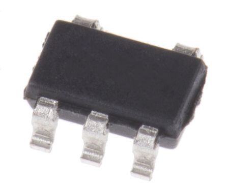
| 产品图片 |
|
| rohs | 符合RoHS无铅 / 符合限制有害物质指令(RoHS)规范要求 |
| 产品系列 | 放大器 IC,运算放大器 - 运放,Analog Devices AD8065ARTZ-REEL7FastFET™ |
| 数据手册 | |
| 产品型号 | AD8065ARTZ-REEL7 |
| 产品培训模块 | http://www.digikey.cn/PTM/IndividualPTM.page?site=cn&lang=zhs&ptm=30008http://www.digikey.cn/PTM/IndividualPTM.page?site=cn&lang=zhs&ptm=26202 |
| 产品目录页面 | |
| 产品种类 | 运算放大器 - 运放 |
| 供应商器件封装 | SOT-23-5 |
| 共模抑制比—最小值 | 100 dB |
| 关闭 | No Shutdown |
| 其它名称 | AD8065ARTZ-REEL7DKR |
| 包装 | Digi-Reel® |
| 压摆率 | 180 V/µs |
| 双重电源电压 | +/- 3 V, +/- 5 V, +/- 9 V |
| 商标 | Analog Devices |
| 增益带宽生成 | 60 MHz |
| 增益带宽积 | - |
| 安装类型 | 表面贴装 |
| 安装风格 | SMD/SMT |
| 封装 | Reel |
| 封装/外壳 | SC-74A,SOT-753 |
| 封装/箱体 | SOT-23-5 |
| 工作温度 | -40°C ~ 85°C |
| 工作电源电压 | 5 V to 24 V |
| 工厂包装数量 | 3000 |
| 技术 | FET |
| 放大器类型 | 电压反馈 |
| 最大双重电源电压 | +/- 12 V |
| 最大工作温度 | + 85 C |
| 最小双重电源电压 | +/- 2.5 V |
| 最小工作温度 | - 40 C |
| 标准包装 | 1 |
| 电压-电源,单/双 (±) | 5 V ~ 24 V, ±2.5 V ~ 12 V |
| 电压-输入失调 | 400µV |
| 电流-电源 | 6.6mA |
| 电流-输入偏置 | 3pA |
| 电流-输出/通道 | 30mA |
| 电源电流 | 7.4 mA |
| 电路数 | 1 |
| 系列 | AD8065 |
| 视频文件 | http://www.digikey.cn/classic/video.aspx?PlayerID=1364138032001&width=640&height=505&videoID=2245193153001 |
| 设计资源 | |
| 转换速度 | 180 V/us |
| 输入偏压电流—最大 | 6 pA |
| 输入参考电压噪声 | 7 nV |
| 输入补偿电压 | 400 uV |
| 输出电流 | 35 mA |
| 输出类型 | 满摆幅 |
| 通道数量 | 1 Channel |


- 商务部:美国ITC正式对集成电路等产品启动337调查
- 曝三星4nm工艺存在良率问题 高通将骁龙8 Gen1或转产台积电
- 太阳诱电将投资9.5亿元在常州建新厂生产MLCC 预计2023年完工
- 英特尔发布欧洲新工厂建设计划 深化IDM 2.0 战略
- 台积电先进制程称霸业界 有大客户加持明年业绩稳了
- 达到5530亿美元!SIA预计今年全球半导体销售额将创下新高
- 英特尔拟将自动驾驶子公司Mobileye上市 估值或超500亿美元
- 三星加码芯片和SET,合并消费电子和移动部门,撤换高东真等 CEO
- 三星电子宣布重大人事变动 还合并消费电子和移动部门
- 海关总署:前11个月进口集成电路产品价值2.52万亿元 增长14.8%


PDF Datasheet 数据手册内容提取
High Performance, 145 MHz FastFET Op Amps Data Sheet AD8065/AD8066 FEATURES APPLICATIONS Qualified for automotive applications Automotive driver assistance systems FET input amplifier Photodiode preamps 1 pA input bias current Filters A/D drivers Low cost Level shifting High speed: 145 MHz, −3 dB bandwidth (G = +1) Buffering 180 V/µs slew rate (G = +2) CONNECTION DIAGRAMS Low noise 7 nV/√Hz (f = 10 kHz) AD8065 AD8065 VOUT 1 5 +VS NC 1 8 NC 0.6 fA/√Hz (f = 10 kHz) Wide supply voltage range: 5 V to 24 V –VS 2 –IN 2 7 +VS Single-supply and rail-to-rail output +IN 3 4 –IN +IN 3 6 VOUT TOP VIEW Low offset voltage 1.5 mV maximum (Not to Scale) –VS 4 TOP VIEW 5 NC High common-mode rejection ratio: −100 dB (Not to Scale) Excellent distortion specifications SFDR −88 dBc @ 1 MHz AD8066 VOUT1 1 8 +VS Low power: 6.4 mA/amplifier typical supply current –IN1 2 7 VOUT2 No phase reversal +IN1 3 6 –IN2 Small packaging: SOIC-8, SOT-23-5, and MSOP-8 –VS 4 (NToOt Pto V SIEcaWle) 5 +IN2 02916-E-001 Figure 1. GENERAL DESCRIPTION The AD8065/AD8066 are high performance, high speed, FET input amplifiers available in small packages: SOIC-8, MSOP-8, The AD8065/AD80661 FastFET™ amplifiers are voltage feedback and SOT-23-5. They are rated to work over the industrial amplifiers with FET inputs offering high performance and ease temperature range of −40°C to +85°C. of use. The AD8065 is a single amplifier, and the AD8066 is a dual amplifier. These amplifiers are developed in the Analog The AD8065WARTZ-R7 is fully qualified for automotive Devices, Inc. proprietary XFCB process and allow exceptionally applications. It is rated to operate over the extended temperature low noise operation (7.0 nV/√Hz and 0.6 fA/√Hz) as well as range (−40°C to +105°C), up to a maximum supply voltage very high input impedance. range of ±5 V only. With a wide supply voltage range from 5 V to 24 V, the ability to 24 operate on single supplies, and a bandwidth of 145 MHz, the 21 G = +10 AD8065/AD8066 are designed to work in a variety of applications. 18 VO = 200mV p-p For added versatility, the amplifiers also contain rail-to-rail outputs. 15 G = +5 Despite the low cost, the amplifiers provide excellent overall B) 12 performance. The differential gain and phase errors of 0.02% N (d 9 and 0.02°, respectively, along with 0.1 dB flatness out to 7 MHz, AI G = +2 G 6 make these amplifiers ideal for video applications. Additionally, they offer a high slew rate of 180 V/µs, excellent distortion (SFDR 3 G = +1 of −88 dBc @ 1 MHz), extremely high common-mode rejection 0 of −100 dB, and a low input offset voltage of 1.5 mV maximum –3 under warmed up conditions. The AD8065/AD8066 operate ucaspinagb loen olyf dae 6li.v4e mrinAg/ aump ptoli f3ie0r mtyApi ocaf ll osuadp pcluyr cruenrrte. nt and are –60.1 1 FREQUE1N0CY (MHz) 100 1000 02916-E-002 Figure 2. Small Signal Frequency Response 1 Protected by U. S. Patent No. 6,262,633. Rev. L Document Feedback Information furnished by Analog Devices is believed to be accurate and reliable. However, no responsibility is assumed by Analog Devices for its use, nor for any infringements of patents or other One Technology Way, P.O. Box 9106, Norwood, MA 02062-9106, U.S.A. rights of third parties that may result from its use. Specifications subject to change without notice. No license is granted by implication or otherwise under any patent or patent rights of Analog Devices. Tel: 781.329.4700 ©2002–2019 Analog Devices, Inc. All rights reserved. Trademarks and registered trademarks are the property of their respective owners. Technical Support www.analog.com
AD8065/AD8066 Data Sheet TABLE OF CONTENTS Features .............................................................................................. 1 Wideband Operation ................................................................. 21 Applications ....................................................................................... 1 Input Protection ......................................................................... 21 Connection Diagrams ...................................................................... 1 Thermal Considerations ............................................................ 22 General Description ......................................................................... 1 Input and Output Overload Behavior ..................................... 22 Revision History ............................................................................... 3 Layout, Grounding, and Bypassing Considerations .................. 23 Specifications ±5 V ........................................................................... 4 Power Supply Bypassing ............................................................ 23 Specifications ±12 V ......................................................................... 6 Grounding ................................................................................... 23 Specifications +5 V ........................................................................... 7 Leakage Currents ........................................................................ 23 Absolute Maximum Ratings ............................................................ 9 Input Capacitance ...................................................................... 23 Maximum Power Dissipation ..................................................... 9 Output Capacitance ................................................................... 23 Output Short Circuit .................................................................... 9 Input-to-Output Coupling ........................................................ 24 ESD Caution .................................................................................. 9 Wideband Photodiode Preamp ................................................ 24 Typical Performance Characteristics ........................................... 10 High Speed JFET Input Instrumentation Amplifier.............. 25 Test Circuits ..................................................................................... 17 Video Buffer ................................................................................ 26 Theory of Operation ...................................................................... 20 Outline Dimensions ....................................................................... 27 Closed-Loop Frequency Response ........................................... 20 Ordering Guide .......................................................................... 28 Noninverting Closed-Loop Frequency Response .................. 20 Automotive Products ................................................................. 28 Inverting Closed-Loop Frequency Response ......................... 20 Rev. L | Page 2 of 28
Data Sheet AD8065/AD8066 REVISION HISTORY Changes to General Description ..................................................... 1 1/2019—Rev. K to Rev. L Changes to Figure 22 through Figure 27 ...................................... 11 Changed AD8065WARTZ-REEL7 to Updated Outline Dimensions ........................................................ 25 AD8065WARTZ-R7 ...................................................... Throughout Changes to Ordering Guide ........................................................... 26 8/2016—Rev. J to Rev. K Updated Outline Dimensions ........................................................ 27 2/2004—Rev. D to Rev. E. Changes to Ordering Guide ........................................................... 28 Updated Format ................................................................ Universal Updated Figure 56 ......................................................................... 21 Updated Outline Dimensions ...................................................... 25 8/2010—Rev. I to Rev. J Updated Ordering Guide ............................................................. 26 Changes to Features Section, Applications Section, and General Description Section ........................................................................... 1 Change to Table 1 .............................................................................. 4 11/2003—Rev. C to Rev. D. Change to Table 3 .............................................................................. 7 Changes to Features ......................................................................... 1 Changes to Table 4 ............................................................................ 9 Changes to Connection Diagrams ................................................. 1 Changes to Figure 9 ......................................................................... 10 Updated Ordering Guide ................................................................ 5 Changes to Inverting Closed-Loop Frequency Response Updated Outline Dimensions ...................................................... 22 Section .............................................................................................. 20 Moved Leakage Currents Section, Input Capacitance Section, and Output Capacitance Section ................................................... 23 4/2003—Rev. B to Rev. C. Moved Input-to-Input Coupling Section, Wideband Added SOIC-8 (R) for the AD8065 ............................................... 4 Photodiode Preamp Section, and Figure 59 ................................ 24 Changes to Table 5 .......................................................................... 25 2/2003—Rev. A to Rev. B. Moved Figure 60 and High Speed JFET Input Instrumentation Changes to Absolute Maximum Ratings....................................... 4 Amplifier Section ............................................................................ 25 Changes to Test Circuit 10 ........................................................... 14 Updated Outline Dimensions ........................................................ 27 Changes to Test Circuit 11 ........................................................... 15 Changes to Ordering Guide ........................................................... 28 Changes to Noninverting Closed-Loop Frequency Response 16 Added Automotive Products Section ........................................... 28 Changes to Inverting Closed-Loop Frequency Response ....... 16 Updated Figure 6 .......................................................................... 18 3/2009—Rev. H to Rev. I Changes to Figure 7 ...................................................................... 19 Changes to High Speed JFET Input Instrumentation Amplifier Changes to Figure 10 .................................................................... 21 Section .............................................................................................. 23 Changes to Figure 11 .................................................................... 22 Updated Outline Dimensions ........................................................ 24 Changes to High Speed JFET Instrumentation Amplifier ...... 22 Changes to Video Buffer .............................................................. 22 9/2008—Rev. G to Rev. H Deleted Usable Range Parameter, Table 1 ...................................... 3 Deleted Usable Range Parameter, Table 2 ...................................... 4 8/2002—Rev. 0 to Rev. A. Deleted Usable Range Parameter, Table 3 ...................................... 5 Added AD8066 .................................................................. Universal Changes to Layout ............................................................................. 6 Added SOIC-8 (R) and MSOP-8 (RM) ......................................... 1 Changes to Input and Output Overload Behavior Section ........ 19 Edits to General Description .......................................................... 1 Changes to Table 5 Expressions Column ..................................... 22 Edits to Specifications ...................................................................... 2 New Figure 2 ..................................................................................... 5 Changes to Ordering Guide ............................................................ 5 1/2006—Rev. F to Rev. G Edits to TPCs 18, 25, and 28 ........................................................... 8 Changes to Ordering Guide ........................................................... 26 New TPC 36 ................................................................................... 11 12/2005—Rev. E to Rev. F Added Test Circuits 10 and 11 .................................................... 14 Updated Format .................................................................. Universal MSOP (RM-8) Added .................................................................. 23 Changes to Features .......................................................................... 1 Rev. L | Page 3 of 28
AD8065/AD8066 Data Sheet SPECIFICATIONS ±5 V @ T = 25°C, V = ±5 V, R = 1 kΩ, unless otherwise noted. A S L Table 1. Parameter Conditions Min Typ Max Unit DYNAMIC PERFORMANCE −3 dB Bandwidth G = +1, V = 0.2 V p-p (AD8065) 100 145 MHz O AD8065WARTZ only: T − T 88 MHz MIN MAX G = +1, V = 0.2 V p-p (AD8066) 100 120 MHz O G = +2, V = 0.2 V p-p 50 MHz O G = +2, V = 2 V p-p 42 MHz O Bandwidth for 0.1 dB Flatness G = +2, V = 0.2 V p-p 7 MHz O Input Overdrive Recovery Time G = +1, −5.5 V to +5.5 V 175 ns Output Recovery Time G = −1, −5.5 V to +5.5 V 170 ns Slew Rate G = +2, V = 4 V step 130 180 V/µs O AD8065WARTZ only: T − T 155 V/µs MIN MAX Settling Time to 0.1% G = +2, V = 2 V step 55 ns O G = +2, V = 8 V step 205 ns O NOISE/HARMONIC PERFORMANCE SFDR f = 1 MHz, G = +2, V = 2 V p-p −88 dBc C O f = 5 MHz, G = +2, V = 2 V p-p −67 dBc C O f = 1 MHz, G = +2, V = 8 V p-p −73 dBc C O Third-Order Intercept f = 10 MHz, R = 100 Ω 24 dBm C L Input Voltage Noise f = 10 kHz 7 nV/√Hz Input Current Noise f = 10 kHz 0.6 fA/√Hz Differential Gain Error NTSC, G = +2, R = 150 Ω 0.02 % L Differential Phase Error NTSC, G = +2, R = 150 Ω 0.02 Degrees L DC PERFORMANCE Input Offset Voltage V = 0 V, SOIC package 0.4 1.5 mV CM AD8065WARTZ only: T − T 2.6 mV MIN MAX Input Offset Voltage Drift 1 17 µV/°C AD8065WARTZ only: T − T 17 µV/°C MIN MAX Input Bias Current SOIC package 2 6 pA T to T 25 125 pA MIN MAX Input Offset Current 1 10 pA T to T 1 125 pA MIN MAX Open-Loop Gain V = ±3 V, R = 1 kΩ 100 113 dB O L AD8065WARTZ only: T − T 100 dB MIN MAX INPUT CHARACTERISTICS Common-Mode Input Impedance 1000 || 2.1 GΩ || pF Differential Input Impedance 1000 || 4.5 GΩ || pF Input Common-Mode Voltage Range FET Input Range −5 to +1.7 −5.0 to +2.4 V AD8065WARTZ only: T − T −5 to +1.7 V MIN MAX Common-Mode Rejection Ratio V = −1 V to +1 V −85 −100 dB CM V = −1 V to +1 V (SOT-23) −82 −91 dB CM AD8065WARTZ only: T − T −82 dB MIN MAX Rev. L | Page 4 of 28
Data Sheet AD8065/AD8066 Parameter Conditions Min Typ Max Unit OUTPUT CHARACTERISTICS Output Voltage Swing R = 1 kΩ −4.88 to +4.90 −4.94 to +4.95 V L AD8065WARTZ only: T − T −4.88 to +4.90 V MIN MAX R = 150 Ω −4.8 to +4.7 V L Output Current V = 9 V p-p, SFDR ≥ −60 dBc, f = 500 kHz 35 mA O Short-Circuit Current 90 mA Capacitive Load Drive 30% overshoot G = +1 20 pF POWER SUPPLY Operating Range 5 24 V AD8065WARTZ only: T − T 5 10 V MIN MAX Quiescent Current per Amplifier 6.4 7.2 mA AD8065WARTZ only: T − T 7.2 mA MIN MAX Power Supply Rejection Ratio ±PSRR −85 −100 dB AD8065WARTZ only: T − T −85 dB MIN MAX Rev. L | Page 5 of 28
AD8065/AD8066 Data Sheet SPECIFICATIONS ±12 V @ T = 25°C, V = ±12 V, R = 1 kΩ, unless otherwise noted. A S L Table 2. Parameter Conditions Min Typ Max Unit DYNAMIC PERFORMANCE −3 dB Bandwidth G = +1, V = 0.2 V p-p (AD8065) 100 145 MHz O G = +1, V = 0.2 V p-p (AD8066) 100 115 MHz O G = +2, V = 0.2 V p-p 50 MHz O G = +2, V = 2 V p-p 40 MHz O Bandwidth for 0.1 dB Flatness G = +2, V = 0.2 V p-p 7 MHz O Input Overdrive Recovery G = +1, −12.5 V to +12.5 V 175 ns Output Overdrive Recovery G = −1, −12.5 V to +12.5 V 170 ns Slew Rate G = +2, V = 4 V step 130 180 V/µs O Settling Time to 0.1% G = +2, V = 2 V step 55 ns O G = +2, V = 10 V step 250 ns O NOISE/HARMONIC PERFORMANCE SFDR f = 1 MHz, G = +2, V = 2 V p-p −100 dBc C O f = 5 MHz, G = +2, V = 2 V p-p −67 dBc C O f = 1 MHz, G = +2, V = 10 V p-p −85 dBc C O Third-Order Intercept f = 10 MHz, R = 100 Ω 24 dBm C L Input Voltage Noise f = 10 kHz 7 nV/√Hz Input Current Noise f = 10 kHz 1 fA/√Hz Differential Gain Error NTSC, G = +2, R = 150 Ω 0.04 % L Differential Phase Error NTSC, G = +2, R = 150 Ω 0.03 Degrees L DC PERFORMANCE Input Offset Voltage V = 0 V, SOIC package 0.4 1.5 mV CM Input Offset Voltage Drift 1 17 µV/°C Input Bias Current SOIC package 3 7 pA T to T 25 pA MIN MAX Input Offset Current 2 10 pA T to T 2 pA MIN MAX Open-Loop Gain V = ±10 V, R = 1 kΩ 103 114 dB O L INPUT CHARACTERISTICS Common-Mode Input Impedance 1000 || 2.1 GΩ || pF Differential Input Impedance 1000 || 4.5 GΩ || pF Input Common-Mode Voltage Range FET Input Range −12 to +8.5 −12.0 to +9.5 V Common-Mode Rejection Ratio V = −1 V to +1 V −85 −100 dB CM V = −1 V to +1 V (SOT-23) −82 −91 dB CM OUTPUT CHARACTERISTICS Output Voltage Swing R = 1 kΩ −11.8 to +11.8 −11.9 to +11.9 V L R = 350 Ω −11.25 to +11.5 V L Output Current V = 22 V p-p, SFDR ≥ −60 dBc, f = 500 kHz 30 mA O Short-Circuit Current 120 mA Capacitive Load Drive 30% overshoot G = +1 25 pF POWER SUPPLY Operating Range 5 24 V Quiescent Current per Amplifier 6.6 7.4 mA Power Supply Rejection Ratio ±PSRR −84 −93 dB Rev. L | Page 6 of 28
Data Sheet AD8065/AD8066 SPECIFICATIONS +5 V @ T = 25°C, V = 5 V, R = 1 kΩ, unless otherwise noted. A S L Table 3. Parameter Conditions Min Typ Max Unit DYNAMIC PERFORMANCE −3 dB Bandwidth G = +1, V = 0.2 V p-p (AD8065) 125 155 MHz O AD8065WARTZ only: T − T 90 MHz MIN MAX G = +1, V = 0.2 V p-p (AD8066) 110 130 MHz O G = +2, V = 0.2 V p-p 50 MHz O G = +2, V = 2 V p-p 43 MHz O Bandwidth for 0.1 dB Flatness G = +2, V = 0.2 V p-p 6 MHz O Input Overdrive Recovery Time G = +1, −0.5 V to +5.5 V 175 ns Output Recovery Time G = −1, −0.5 V to +5.5 V 170 ns Slew Rate G = +2, V = 2 V step 105 160 V/µs O AD8065WARTZ only: T − T 123 V/µs MIN MAX Settling Time to 0.1% G = +2, V = 2 V step 60 ns O NOISE/HARMONIC PERFORMANCE SFDR f = 1 MHz, G = +2, V = 2 V p-p −65 dBc C O f = 5 MHz, G = +2, V = 2 V p-p −50 dBc C O Third-Order Intercept f = 10 MHz, R = 100 Ω 22 dBm C L Input Voltage Noise f = 10 kHz 7 nV/√Hz Input Current Noise f = 10 kHz 0.6 fA/√Hz Differential Gain Error NTSC, G = +2, R = 150 Ω 0.13 % L Differential Phase Error NTSC, G = +2, R = 150 Ω 0.16 Degrees L DC PERFORMANCE Input Offset Voltage V = 1.0 V, SOIC package 0.4 1.5 mV CM AD8065WARTZ only: T − T 2.6 mV MIN MAX Input Offset Voltage Drift 1 17 µV/ºC AD8065WARTZ only: T − T 17 µV/ºC MIN MAX Input Bias Current SOIC package 1 5 pA T to T 25 125 pA MIN MAX Input Offset Current 1 5 pA T to T 1 125 pA MIN MAX Open-Loop Gain V = 1 V to 4 V (AD8065) 100 113 dB O AD8065WARTZ only: T − T 100 dB MIN MAX V = 1 V to 4 V (AD8066) 90 103 dB O INPUT CHARACTERISTICS Common-Mode Input Impedance 1000 || 2.1 GΩ || pF Differential Input Impedance 1000 || 4.5 GΩ || pF Input Common-Mode Voltage Range FET Input Range 0 to 1.7 0 to 2.4 V AD8065WARTZ only: T − T 0 to 1.7 V MIN MAX Common-Mode Rejection Ratio V = 0.5 V to 1.5 V −74 −100 dB CM V = 1 V to 2 V (SOT-23) −78 −91 dB CM AD8065WARTZ only: T -T −76 dB MIN MAX OUTPUT CHARACTERISTICS Output Voltage Swing R = 1 kΩ 0.1 to 4.85 0.03 to 4.95 V L AD8065WARTZ only: T − T 0.1 to 4.85 V MIN MAX R = 150 Ω 0.07 to 4.83 V L Output Current V = 4 V p-p, SFDR ≥ −60 dBc, f = 500 kHz 35 mA O Short-Circuit Current 75 mA Capacitive Load Drive 30% overshoot G = +1 5 pF Rev. L | Page 7 of 28
AD8065/AD8066 Data Sheet Parameter Conditions Min Typ Max Unit POWER SUPPLY Operating Range 5 24 V AD8065WARTZ only: T − T 5 10 V MIN MAX Quiescent Current per Amplifier 5.8 6.4 7.0 mA AD8065WARTZ only: T − T 7.0 mA MIN MAX Power Supply Rejection Ratio ±PSRR −78 −100 dB AD8065WARTZ only: T − T −78 dB MIN MAX Rev. L | Page 8 of 28
Data Sheet AD8065/AD8066 ABSOLUTE MAXIMUM RATINGS Table 4. RMS output voltages should be considered. If RL is referenced to Parameter Rating VS−, as in single-supply operation, then the total drive power is Supply Voltage 26.4 V VS × IOUT. Power Dissipation See Figure 3 If the rms signal levels are indeterminate, then consider the Common-Mode Input Voltage VEE − 0.5 V to VCC + 0.5 V worst case, when VOUT = VS/4 for RL to midsupply. Differential Input Voltage 1.8 V ( ) Storage Temperature Range −65°C to +125°C P =(V ×I )+ VS/42 D S S R Operating Temperature Range −40°C to +85°C L AD8065WARTZ Only −40°C to +105°C In single-supply operation with R referenced to V−, worst case L S Lead Temperature 300°C is V = V/2. OUT S (Soldering, 10 sec) 2.0 Stresses at or above those listed under Absolute Maximum Ratings may cause permanent damage to the product. This is a W) N ( stress rating only; functional operation of the product at these O 1.5 TI or any other conditions above those indicated in the operational PA MSOP-8 SI section of this specification is not implied. Operation beyond S SOIC-8 DI the maximum operating conditions for extended periods may R 1.0 E W affect product reliability. O SOT-23-5 P M MAXIMUM POWER DISSIPATION U M 0.5 XI The maximum safe power dissipation in the AD8065/AD8066 A M packages is limited by the associated rise in junction temperature tg(hTlaeJ)s jsou tnnr actnthisoei ntdi oiteen.m Ttephmeer papetluraasrtetui.c rA eet,n tachpaepp rpsoulaxlasitmtiicna gcte htlhayn e1 gd5e0ise° iCltos, c pwarlholyipc reher aitsice htshe. es 0–60 –40 –2A0MBIEN0T TEM2P0ERATU4R0E (°C)60 80 100 02916-E-003 Figure 3. Maximum Power Dissipation vs. Temperature for a 4-Layer Board Even temporarily exceeding this temperature limit can change the stresses that the package exerts on the die, permanently Airflow increases heat dissipation, effectively reducing θ . Also, JA shifting the parametric performance of the AD8065/AD8066. more metal directly in contact with the package leads from Exceeding a junction temperature of 175°C for an extended metal traces, through holes, ground, and power planes reduce time can result in changes in the silicon devices, potentially the θ . Care must be taken to minimize parasitic capacitances JA causing failure. at the input leads of high speed op amps as discussed in the Layout, Grounding, and Bypassing Considerations section. The still air thermal properties of the package and PCB (θ ), JA ambient temperature (TA), and total power dissipated in the Figure 3 shows the maximum safe power dissipation in the package (PD) determine the junction temperature of the die. package vs. the ambient temperature for the SOIC (125°C/W), The junction temperature can be calculated by SOT-23 (180°C/W), and MSOP (150°C/W) packages on a JEDEC standard 4-layer board. θ values are approximations. T = T + (P × θ ) JA J A D JA OUTPUT SHORT CIRCUIT The power dissipated in the package (P ) is the sum of the D quiescent power dissipation and the power dissipated in the Shorting the output to ground or drawing excessive current for package due to the load drive for all outputs. The quiescent the AD8065/AD8066 will likely cause catastrophic failure. power is the voltage between the supply pins (V) times the S quiescent current (I). Assuming the load (R) is referenced to S L midsupply, then the total drive power is V /2 × I , some of ESD CAUTION S OUT which is dissipated in the package and some in the load (V × OUT I ). The difference between the total drive power and the load OUT power is the drive power dissipated in the package. ( ) P =QuiescentPower+ TotalDrivePower−LoadPower D P =(V ×I )+VS ×VOUT −VOUT2 D S S 2 R R L L Rev. L | Page 9 of 28
AD8065/AD8066 Data Sheet TYPICAL PERFORMANCE CHARACTERISTICS Default Conditions: ±5 V, C = 5 pF, R = 1 kΩ, V = 2 V p-p, Temperature = 25°C. L L OUT 24 6.9 RL = 150Ω 21 G = +10 6.8 G = +2 VO = 200mV p-p VOUT = 0.2V p-p 18 6.7 VOUT = 0.7V p-p 15 G = +5 6.6 B) 12 B) 6.5 VOUT = 1.4V p-p d d N ( 9 N ( 6.4 AI G = +2 AI G 6 G 6.3 3 6.2 G = +1 0 6.1 –3 6.0 –60.1 1 FREQUE1N0CY (MHz) 100 1000 02916-E-004 5.90.1 1FREQUENCY (MHz)10 100 02916-E-007 Figure 4. Small Signal Frequency Response for Various Gains Figure 7. 0.1 dB Flatness Frequency Response (See Figure 43) 6 9 VO = 200mV p-p VO = 200mV p-p G = +1 G = +2 4 8 VS = +5V VS = +5V 2 7 VS =±5V B) VS =±5V B) d d N ( 0 N ( 6 GAI VS =±12V GAI VS =±12V –2 5 –4 4 –60.1 1 FREQUE1N0CY (MHz) 100 1000 02916-E-005 30.1 1 FREQUE1N0CY (MHz) 100 1000 02916-E-008 Figure 5. Small Signal Frequency Response for Various Supplies Figure 8. Small Signal Frequency Response for Various Supplies (See Figure 42) (See Figure 43) 2 8 VO = 2V p-p VO = 2V p-p 1 G = +1 7 G = +2 VS = +5V VS = ±5V 6 0 VS = ±12V VS =±5V 5 GAIN (dB) ––21 VS =±12V GAIN (dB) 4 3 –3 2 –4 1 –50.1 1 FREQUE1N0CY (MHz) 100 1000 02916-E-006 00.1 1 FREQUE1N0CY (MHz) 100 1000 02916-009 Figure 6. Large Signal Frequency Response for Various Supplies Figure 9. Large Signal Frequency Response for Various Supplies (See Figure 42) (See Figure 43) Rev. L | Page 10 of 28
Data Sheet AD8065/AD8066 9 8 VO = 200mV p-p CL = 25pF G = +1 RSNUB = 20Ω 6 6 CL = 25pF CL = 5pF CL = 55pF 4 3 CL = 20pF CL = 25pF 2 GAIN (dB) 0 GAIN (dB) 0 CL = 5pF –2 –3 –4 –6 VO = 200mV p-p –6 G = +2 –90.1 1 FREQUE1N0CY (MHz) 100 1000 02916-E-010 –80.1 1 FREQUE1N0CY (MHz) 100 1000 02916-E-013 Figure 10. Small Signal Frequency Response for Various CLOAD (See Figure 42) Figure 13. Small Signal Frequency Response for Various CLOAD (See Figure 43) 8 8 VOUT = 0.2V p-p 6 7 RL = 100Ω G = +2 VOUT = 2V p-p 4 6 2 5 RL = 1kΩ B) B) N (d 0 VOUT = 4V p-p N (d 4 AI AI G G –2 3 –4 2 VO = 200mV p-p –6 1 G = +2 –80.1 1 FREQUE1N0CY (MHz) 100 1000 02916-E-011 00.1 1 FREQUE1N0CY (MHz) 100 1000 02916-E-014 Figure 11. Frequency Response for Various Output Amplitudes Figure 14. Small Signal Frequency Response for Various RLOAD (See Figure 43) (See Figure 43) 14 80 120 VO = 200mV p-p 12 G = +2 PHASE 10 RF = RG = 1kΩ, 60 60 RS = 500Ω B) GAIN (dB) 2468 RF =R RSG = = 5 010kΩΩ,, RRRRCFSFFS ===== RR222.55GG200 p==ΩΩF ,550000ΩΩ,, PEN-LOOP GAIN (d 2400 GAIN –060 PHASE (DEGREES) CF = 3.3pF O 0 0 –120 –2 –40.1 1 FREQUE1N0CY (MHz) 100 1000 02916-E-012 –200.01 0.1 FR1EQUENCY (M10Hz) 100 100–0180 02916-E-015 Figure 12. Small Signal Frequency Response for Various RF/CF (See Figure 43) Figure 15. Open-Loop Response Rev. L | Page 11 of 28
AD8065/AD8066 Data Sheet –30 –40 –40 G = +2 –50 –50 –60 Bc) –60 Bc) HD2 G = +2 ON (d –70 HD2 RL = 150Ω ON (d –70 HD3 G = +2 STORTI –80 HD2 RL = 1kΩ HD3 RL = 1kΩ STORTI –80 HD2 G = +1 DI –90 DI –100 HD3 RL = 150Ω –90 HD3 G = +1 –100 –110 –1200.1 1FREQUENCY (MHz)10 100 02916-E-016 –1100.1 1FREQUENCY (MHz)10 100 02916-E-019 Figure 16. Harmonic Distortion vs. Frequency for Various Loads Figure 19. Harmonic Distortion vs. Frequency for Various Gains (See Figure 43) (See Figure 42 and Figure 43) –30 –20 –40 G = +2 –30 VGS = = +±212V –50 VF S= =1M±1H2zV –40 HD2 VO = 20V p-p Bc) –60 Bc) –50 HD3 VO = 20V p-p ON (d –70 HD2 RL = 150Ω ON (d –60 HD2 VO = 10V p-p STORTI –80 HD3 RL = 150Ω STORTI ––8700 HD3 VO = 10V p-p DI –90 HD2 RL = 300Ω DI –90 –100 –100 HD2 VO = 2V p-p HD3 RL = 300Ω –110 –110 HD3 VO = 2V p-p –1200 1 2 3 4OUT5PUT6 AM7PLIT8UDE9 (V1 p0-p1)1 12 13 14 15 02916-E-017 –1200.1 FREQUE1N.0CY (MHz) 10.0 02916-E-020 Figure 17. Harmonic Distortion vs. Amplitude for Various Loads VS = ±12 V Figure 20. Harmonic Distortion vs. Frequency for Various Amplitudes (See Figure 43) (See Figure 43) 50 100 RL = 100Ω 45 VS =±12V m) 40 T (dB VS =±5V Hz) OIN 35 V/ RCEPT P 30 VS = +5V NOISE (n 10 E NT 25 I 20 151 FREQUENCY (MHz) 10 02916-E-018 110 100 1k 1F0RkEQU1E0N0kCY (H1zM) 10M 100M 1G 02916-E-021 Figure 18. Third-Order Intercept vs. Frequency and Supply Voltage Figure 21. Voltage Noise Rev. L | Page 12 of 28
Data Sheet AD8065/AD8066 G = +1 CL = 20pF G = +1 CL = 5pF 50mV/DIV 25ns/DIV 50mV/DIV 25ns/DIV 02916-022 02916-025 Figure 22. Small Signal Transient Response 5 V Supply (See Figure 42) Figure 25. Small Signal Transient Response ±5 V (See Figure 42) G = +1 G5 =µ +s2 VS =±12V VOUT = 10V p-p VOUT = 10V p-p VS =±12V VOUT = 4V p-p VOUT = 2V p-p VOUT = 2V p-p 2V/DIV 50ns/DIV 2V/DIV 50ns/DIV 02916-023 02916-026 Figure 23. Large Signal Transient Response (See Figure 42) Figure 26. Large Signal Transient Response (See Figure 43) G =–1 G = +1 VS =±5V VS =±5V 2.0V/DIV 100ns/DIV 2.0V/DIV 100ns/DIV 02916-024 02916-027 Figure 24. Output Overdrive Recovery (See Figure 44) Figure 27. Input Overdrive Recovery (See Figure 42) Rev. L | Page 13 of 28
AD8065/AD8066 Data Sheet VIN = 140mV/DIV VIN= 500mV/DIV VOUT– 2VIN +0.1% +0.1% –0.1% t =0 –0.1% t =0 VOUT– 2VIN 2mV/DIV 10ns/DIV 2mV/DIV 64µs/DIV 02916-E-028 02916-E-031 Figure 28. Long-Term Settling Time (See Figure 49) Figure 31. 0.1% Short-Term Settling Time (See Figure 49) 0 42 E 36 +Ib AG 30 T ENT (pA) –1–05 –Ib µI(A)b 21164820 –Ib BJT INPUT S R R 10 U S C –15 5 –Ib E INPUT BIA –20 +Ib I (pA)b ––1–15500 +Ib NPUT STAG –25 T I –20 E F –25 –3025 35 45TEMPERA55TURE (°C6)5 75 85 02916-E-029 –30–12 –10 –8 –6CO–M4MO–N2-MOD0EVO2LTAG4E (V)6 8 10 12 02916-E-032 Figure 29. Input Bias Current vs. Temperature Figure 32. Input Bias Current vs. Common-Mode Voltage Range (See the Input and Output Overload Behavior Section) 0.3 40 N = 299 35 SD = 0.388 0.2 MEAN =–0.069 V) 30 AGE (m 0.1 VS = +5V 25 T OL 0 VS =±5V 20 V T SE 15 FF –0.1 VS =±12V O 10 –0.2 5 –0.3–14–12–10 –8 C–O6MM–4ON–-M2OD0E VO2LTA4GE (6V) 8 10 12 14 02916-E-030 0–2.0 –1.5 –1I.N0PUT– 0O.F5FSET 0VOLTA0G.5E (mV1).0 1.5 2.0 02916-E-033 Figure 30. Input Offset Voltage vs. Common-Mode Voltage Figure 33. Input Offset Voltage Rev. L | Page 14 of 28
Data Sheet AD8065/AD8066 –30 100 –40 10 –50 ΩE () C dB) –60 DAN 1 G = +1 CMRR ( –70 VS =±12V UT IMPE 0.1 G = +2 P T –80 OU 0.01 –90 VS =±5V –1000.1 1FREQUENCY (MHz)10 100 02916-E-034 0100 1k 10kFREQU1E0N0kCY (Hz)1M 10M 100M 02916-E-037 Figure 34. CMRR vs. Frequency (See Figure 46) Figure 37. Output Impedance vs. Frequency (See Figure 45 and Figure 47) 0.30 80 OLTAGE (V) 00..2205 VCC– VOH OLTAGE (mV) 70 VCC– VOH ON V ON V 60 OUTPUT SATURATI 000...011505 VOL– VEE OUTPUT SATURATI 4500 VOL– VEE 00 10 ILOA2D0 (mA) 30 40 02916-E-035 3025 35 45TEMPERA55TURE (°C6)5 75 85 02916-E-038 Figure 35. Output Saturation Voltage vs. Output Load Current Figure 38. Output Saturation Voltage vs. Temperature 0 0 –10 –10 VGI N= =+ 12V p-p –20 –20 –30 –PSRR B) –30 d SRR (dB) ––5400 +PSRR SSTALK ( ––5400 P –60 O R C –60 B TO A –70 –70 –80 A TO B –90 –80 –1000.01 0.1 FR1EQUENCY (M10Hz) 100 1000 02916-E-036 –900.1 1 FREQUENCY (M1H0z) 100 02916-E-039 Figure 36. PSRR vs. Frequency (See Figure 48 and Figure 50) Figure 39. Crosstalk vs. Frequency (See Figure 51) Rev. L | Page 15 of 28
AD8065/AD8066 Data Sheet 6.60 125 VS =±12V 120 6.55 VS =±5V RENT (mA) 66..4550 GAIN (dB) 111011505 VS =±12V UR VS = +5V OP Y C 6.40 LO 100 VS = +5V SUPPL 6.35 OPEN- 95 VS =±5V 90 6.30 85 6.25–40 –20 0TEMPERA20TURE (°C4)0 60 80 02916-E-040 800 10 ILOA2D0 (mA) 30 40 02916-E-041 Figure 40. Quiescent Supply Current vs. Temperature for Various Figure 41. Open-Loop Gain vs. Load Current for Various Supply Voltages Supply Voltages Rev. L | Page 16 of 28
Data Sheet AD8065/AD8066 TEST CIRCUITS SOIC-8 Pinout +VCC +VCC 4.7µF 4.7µF 0.1µF 0.1µF 24.9Ω 2.2pF 499Ω 499Ω VIN 49.9Ω RSNUB FET PROBE FET PROBE AD8065 AD8065 VIN 49.9Ω 0.1µF 1kΩ CLOAD 249Ω 0.1µF 1kΩ –VEE 4.7µF 02916-E-042 –VEE 4.7µF 02916-E-044 Figure 42. G = +1 Figure 44. G = −1 +VCC +VCC 4.7µF 4.7µF 0.1µF 0.1µF 2.2pF 24.9Ω 499Ω 499Ω FET PROBE RSNUB AD8065 AD8065 VIN NETWORK ANALYZER S22 49.9Ω 249Ω 0.1µF 1kΩ CLOAD 0.1µF 4.7µF 4.7µF –VEE 02916-E-043 –VEE 02916-E-045 Figure 43. G = +2 Figure 45. Output Impedance G = +1 Rev. L | Page 17 of 28
AD8065/AD8066 Data Sheet +VCC VIN 4.7µF 1V p-p +VCC 49.9Ω 0.1µF 24.9Ω 499Ω 499Ω VIN FET PROBE FET PROBE AD8065 AD8065 49.9Ω 499Ω 499Ω 0.1µF 1kΩ 0.1µF 1kΩ 4.7µF 4.7µF –VEE 02916-E-046 –VEE 02916-E-048 Figure 46. CMRR Figure 48. Positive PSRR +VCC +VCC 4.7µF 4.7µF 0.1µF 0.1µF 2.2pF 499Ω 499Ω 499Ω 499Ω AD8065 249Ω NETWORKANALYZER 976Ω TO SCOPE S22 AD8065 249Ω 0.1µF VIN 0.1µF 49.9Ω 49.9Ω 4.7µF –VEE 02916-E-047 –VEE 4.7µF 02916-E-049 Figure 47. Output Impedance G = +2 Figure 49. Settling Time Rev. L | Page 18 of 28
Data Sheet AD8065/AD8066 +VCC 2.2pF 4.7µF 499Ω 499Ω 0.1µF 5V 24.9Ω 1.5V 4.7µF 0.1µF FET PROBE AD8065 FET PROBE 249Ω AD8065 VIN 1kΩ 1kΩ 49.9Ω 49.9Ω 1.5V 1.5V 02916-E-052 VIN 1V p-p –VEE 02916-E-050 Figure 50. Negative PSRR Figure 52. Single Supply 24.9Ω FET PROBE 24.9Ω AD8066 +5V 4.7µF 1kΩ 0.1µF RECEIVE SIDE AD8066 VIN 0.1µF 1kΩ 49.9Ω 4.7µF DR–I5VVE SIDE 02916-E-051 Figure 51. Crosstalk—AD8066 Rev. L | Page 19 of 28
AD8065/AD8066 Data Sheet THEORY OF OPERATION The AD8065/AD8066 are voltage feedback operational amplifiers NONINVERTING CLOSED-LOOP FREQUENCY that combine a laser-trimmed JFET input stage with the Analog RESPONSE Devices eXtra Fast Complementary Bipolar (XFCB) process, Solving for the transfer function resulting in an outstanding combination of precision and speed. Ta hpea tseunptepdly r vaoill-ttaog-er arial noguet pisu ftr sotmag e5 cVa ptoab 2le4 oVf. dTrhivei anmg pwliitfhieirns 0fe.5a tVur e VVOI =(RF2+πR×G)fscr+oss2ovπer×(RfGcro+ssoRverF×) RG of either power supply while sourcing or sinking up to 30 mA. where f is the frequency where the amplifier’s open-loop crossover Also featured is a single-supply input stage that handles common- gain equals 0 db mode signals from below the negative supply to within 3 V of the V R +R positive rail. Operation beyond the JFET input range is possible At dc O = F G V R because of an auxiliary bipolar input stage that functions with I G input voltages up to the positive supply. The amplifiers operate as Closed-loop −3 dB frequency if they have a rail-to-rail input and exhibit no phase reversal R behavior for common-mode voltages within the power supply. f = f × G −3dB crossover R +R F G With voltage noise of 7 nV/√Hz and −88 dBc distortion for INVERTING CLOSED-LOOP FREQUENCY 1 MHz, 2 V p-p signals, the AD8065/AD8066 are a great choice RESPONSE for high resolution data acquisition systems. Their low noise, sub-pA input current, precision offset, and high speed make VO = −2π× fcrossover×RF them superb preamps for fast photodiode applications. The VI s(RF +RG)+2π× fcrossover×RG speed and output drive capability of the AD8065/AD8066 also V R O =− F make them useful in video applications. V R At dc I G CLOSED-LOOP FREQUENCY RESPONSE Closed-loop −3 dB frequency The AD8065/AD8066 are classic voltage feedback amplifiers R with an open-loop frequency response that can be approximated as f = f × G the integrator response shown in Figure 53. Basic closed-loop −3dB crossover RF +RG frequency response for inverting and noninverting configurations can be derived from the schematics shown. RF RF RG VI RG VO VO VI VE A VE A 80 A = (2π×fcrossover)/s B)60 d A) ( N ( AI G P 40 O O L N- E OP20 fcrossover= 65MHz 0 0.01 0.1 1 10 100 02916-E-053 FREQUENCY (MHz) Figure 53. Open-Loop Gain vs. Frequency and Basic Connections Rev. L | Page 20 of 28
Data Sheet AD8065/AD8066 The closed-loop bandwidth is inversely proportional to the noise Actual distortion performance depends on a number of gain of the op amp circuit, (R + R )/R . This simple model is variables: F G G accurate for noise gains above 2. The actual bandwidth of circuits • The closed-loop gain of the application with noise gains at or below 2 is higher than those predicted • Whether it is inverting or noninverting with this model due to the influence of other poles in the • Amplifier loading frequency response of the real op amp. • Signal frequency and amplitude RF • Board layout RG +VOS– Also see Figure 16 to Figure 20. The lowest distortion is obtained with the AD8065 used in low gain inverting applications, VO VI RS Ib– A bloeocpa ugsaei nths irse esulilmt iinn awteosr sceo mdimstoornt-iomno pdeer efoffremctasn. Hcei.g her closed- Ib+ 02916-E-054 ITNhPe UinTpu PtsR oOf tThEe CATDI8O0N65 /AD8066 are protected with back-to- Figure 54. Voltage Feedback Amplifier DC Errors back diodes between the input terminals as well as ESD diodes Figure 54 shows a voltage feedback amplifier’s dc errors. For to either power supply. This results in an input stage with picoamps both inverting and noninverting configurations of input current that can withstand up to 1500 V ESD events (human body model) with no degradation. R +R R +R V (error)=I ×R G F −I ×R +V G F O b+ S RG b− F OS RG Excessive power dissipation through the protection devices destroys or degrades the performance of the amplifier. Differ- The voltage error due to I and I is minimized if R = R || R b+ b– S F G ential voltages greater than 0.7 V result in an input current of (though with the AD8065 input currents at typically less than approximately (|V − V | 0.7 V)/R, where R is the resistance in + − I I 20 pA over temperature, this is likely not a concern). To include series with the inputs. common-mode and power supply rejection effects, total V can be OS For input voltages beyond the positive supply, the input current modeled is approximately (V − V − 0.7)/R. Beyond the negative supply, I CC I ΔV ΔV V =V + S + CM the input current is about (VI − VEE + 0.7)/RI. If the inputs of the OS OSnom PSR CMR amplifier are to be subjected to sustained differential voltages V is the offset voltage specified at nominal conditions, greater than 0.7 V, or to input voltages beyond the amplifier OSnom power supply, input current should be limited to 30 mA by an ΔV is the change in power supply from nominal conditions, S appropriately sized input resistor (R), as shown in Figure 55. PSR is the power supply rejection, ΔV is the change in common- I CM mmooddee vroejlteacgteio fnro. m nominal conditions, and CMR is the common- RI>(|V+–V3–0 |m–A 0.7V) RI> (VI–3V0EmEA– 0.7V) WIDEBAND OPERATION FOR LARGE |V+–V–| RI> (VI–V3E0Em+A 0.7V) AD8065 FORVI BEYOND Figure 42 through Figure 44 show the circuits used for wideband RI SUPPLY VOLTAGES characterization for gains of +1, +2, and −1. Source impedance at VI VO trheesp sounmsme winigth ju tnhcet iaomn p(lRifFi |e|r R’s Gi)n fpourmt csa ap apcoiltea ninc eth oef a6m.6p pliFf.i eTrh’s ilso op 02916-E-055 can cause peaking and ringing if the time constant formed is too Figure 55. Current-Limiting Resistor low. Feedback resistances of 300 Ω to 1 kΩ are recommended, because they do not unduly load down the amplifier, and the time constant formed will not be too low. Peaking in the frequency response can be compensated for with a small capacitor (C) in parallel with the feedback resistor, as F illustrated in Figure 12. This shows the effect of different feedback capacitances on the peaking and bandwidth for a noninverting G = +2 amplifier. For the best settling times and the best distortion, the impedances at the AD8065/AD8066 input terminals should be matched. This minimizes nonlinear common-mode capacitive effects that can degrade ac performance. Rev. L | Page 21 of 28
AD8065/AD8066 Data Sheet THERMAL CONSIDERATIONS INPUT AND OUTPUT OVERLOAD BEHAVIOR With 24 V power supplies and 6.5 mA quiescent current, the A simplified schematic of the AD8065/AD8066 input stage is AD8065 dissipates 156 mW with no load. The AD8066 dissipates shown in Figure 56. This shows the cascoded N-channel JFET 312 mW. This can lead to noticeable thermal effects, especially input pair, the ESD and other protection diodes, and the in the small SOT-23-5 (thermal resistance of 160°C/W). V auxiliary NPN input stage that eliminates any phase inversion OS temperature drift is trimmed to guarantee a maximum drift of behavior. When the common-mode input voltage to the amplifier 17 µV/°C, so it can change up to 0.425 mV due to warm-up is driven to within approximately 3 V of the positive power supply, effects for an AD8065/AD8066 in a SOT-23-5 package on 24 V. the input JFET’s bias current turns off and the bias of the NPN pair turns on, taking over control of the amplifier. The NPN I increases by a factor of 1.7 for every 10°C rise in temperature. b differential pair now sets the amplifier’s offset, and the input I is close to five times higher at 24 V supplies as opposed to a b bias current is now in the range of several tens of microamps. single 5 V supply. This behavior is shown in Figure 32. Normal operation resumes Heavy loads increase power dissipation and raise the chip when the common-mode voltage goes below the 3 V from the junction temperature as described in the Maximum Power positive supply threshold. Dissipation section. Care should be taken not to exceed the The output transistors of the rail-to-rail output stage have rated power dissipation of the package. circuitry to limit the extent of their saturation when the output is overdriven. This helps output recovery time. Output recovery from a 0.5 V output overdrive on a ±5 V supply is shown in Figure 24. VCC R1 R5 TO REST OF AMP VTHRESHOLD Q2 Q5 VBIAS D1 R6 R3 Q1 Q6 VN D3 D2 D4 VP Q3 Q4 S R4 R7 S R2 R8 Q7 IT1 IT2 –VEE 02916-E-056 Figure 56. Simplified Input Stage Rev. L | Page 22 of 28
Data Sheet AD8065/AD8066 LAYOUT, GROUNDING, AND BYPASSING CONSIDERATIONS POWER SUPPLY BYPASSING inputs and surrounding area to set up any leakage currents. For the guard ring to be completely effective, it must be driven Power supply pins are actually inputs and care must be taken so by a relatively low impedance source and should completely that a noise-free stable dc voltage is applied. The purpose of bypass surround the input leads on all sides, above and below, using capacitors is to create low impedances from the supply to ground at a multilayer board. all frequencies, thereby shunting or filtering most of the noise. Another effect that can cause leakage currents is the charge Decoupling schemes are designed to minimize the bypassing absorption of the insulator material itself. Minimizing the impedance at all frequencies with a parallel combination of amount of material between the input leads and the guard ring capacitors. 0.1 µF (X7R or NPO) chip capacitors are critical helps to reduce the absorption. Also, low absorption materials, and should be as close as possible to the amplifier package. such as Teflon® or ceramic, could be necessary in some instances. The 4.7 µF tantalum capacitor is less critical for high frequency INPUT CAPACITANCE bypassing, and, in most cases, only one is needed per board at the supply inputs. Along with bypassing and ground, high speed amplifiers can be GROUNDING sensitive to parasitic capacitance between the inputs and ground. A few pF of capacitance reduces the input impedance at high A ground plane layer is important in densely packed PC boards frequencies, in turn increasing the amplifier’s gain, causing peaking to spread the current minimizing parasitic inductances. However, of the frequency response or even oscillations, if severe enough. an understanding of where the current flows in a circuit is critical It is recommended that the external passive components connected to implementing effective high speed circuit design. The length to the input pins be placed as close as possible to the inputs to of the current path is directly proportional to the magnitude of avoid parasitic capacitance. The ground and power planes must parasitic inductances and, therefore, the high frequency impedance be kept at a small distance from the input pins on all layers of of the path. High speed currents in an inductive ground return the board. create unwanted voltage noise. OUTPUT CAPACITANCE The length of the high frequency bypass capacitor leads is most To a lesser extent, parasitic capacitances on the output can cause critical. A parasitic inductance in the bypass grounding works against the low impedance created by the bypass capacitor. Place peaking and ringing of the frequency response. There are two the ground leads of the bypass capacitors at the same physical methods to effectively minimize their effect: location. Because load currents flow from the supplies as well, • As shown in Figure 57, put a small value resistor (R) in S the ground for the load impedance should be at the same physical series with the output to isolate the load capacitor from the location as the bypass capacitor grounds. For the larger value amp’s output stage. A good value to choose is 20 Ω (see capacitors, which are effective at lower frequencies, the current Figure 10). return path distance is less critical. • Increase the phase margin with higher noise gains or add LEAKAGE CURRENTS a pole with a parallel resistor and capacitor from −IN to the output. Poor PC board layout, contaminants, and the board insulator material can create leakage currents that are much larger than the input bias current of the AD8065/AD8066. Any voltage differential between the inputs and nearby runs sets up leakage RS= 20Ω currents through the PC board insulator, for example, 1 V/100 GΩ AD8065 VO = 10 pA. Similarly, any contaminants on the board can create VI CL sleigankaifgicea snigt nleifaikcaagnet l(ys, kpiunt oai lgsu aarred a r cinogm (mshoienl dp)r oabroleumnd). tThoe riendpuuctes 02916-E-057 and input leads that are driven to the same voltage potential as Figure 57. Output Isolation Resistor the inputs. This way there is no voltage potential between the Rev. L | Page 23 of 28
AD8065/AD8066 Data Sheet CF RF IPHOTO RSH= 1011Ω CM CS CD CM VO VB CF+CS RF 02916-E-058 Figure 58. Wideband Photodiode Preamp INPUT-TO-OUTPUT COUPLING The frequency response in this case shows about 2 dB of peaking and 15% overshoot. Doubling C and cutting the F To minimize capacitive coupling between the inputs and output, bandwidth in half results in a flat frequency response with the output signal traces should not be parallel with the inputs. about 5% transient overshoot. WIDEBAND PHOTODIODE PREAMP The preamp’s output noise over frequency is shown in Figure 59. Figure 58 shows an I/V converter with an electrical model of a photodiode. The basic transfer function is 1 I ×R f1= 2πRF(CF+CS+CM+2CD) V = PHOTO F wpahrearlele OIl PUcHToOmTO bisi1n t+ahtesiCo onFu RtopFf uRtF c aunrdre CntF osef ttsh teh pe hsoigtnoadli obdaen,d awnidd tthh.e E (nV/Hz) ff32== 2π(CR1SF+CFCM+2fCCRD+CF)/CF S The stable bandwidth attainable with this preamp is a function NOI E of RF, the gain bandwidth product of the amplifier, and the total TAG RF NOISE L caanpda tchitea namcep alitf itehre ianmpuptl icfiaepra’sc situamncme.i nRgF jaunndc tthioen t,o itnacl lcuadpinacgi tCanS ce VO f2 VEN (CF+CS+CM+ 2CD)/CF f3 produce a pole in the amplifier’s loop transmission that can f1 result in peaking and instability. Adding C creates a 0 in the F lroeodpu ctersa nthsme sisigsinoanl bthaantd cwoimdtphe.n Ist actaens fboer sthhoew pno lteh’sa et ftfhecet s aignnda l VEN NOISE DUE TO AFMRPELQIFUIEENRCY (Hz) 02916-E-059 bandwidth resulting in a 45° phase margin (f ) is defined by Figure 59. Photodiode Voltage Noise Contributions (45) f f = CR The pole in the loop transmission translates to a 0 in the (45) 2π×R ×C F S amplifier’s noise gain, leading to an amplification of the input voltage noise over frequency. The loop transmission 0 where f is the amplifier crossover frequency, R is the feedback CR F introduced by C limits the amplification. The noise gain resistor, and C is the total capacitance at the amplifier summing F S bandwidth extends past the preamp signal bandwidth and is junction (amplifier + photodiode + board parasitics). eventually rolled off by the decreasing loop gain of the The value of C that produces f can be shown to be F (45) amplifier. Keeping the input terminal impedances matched is C recommended to eliminate common-mode noise peaking C = S F 2π×R ×f effects, which adds to the output noise. F CR Integrating the square of the output voltage noise spectral density over frequency and then taking the square root allows users to obtain the total rms output noise of the preamp. Table 5 summarizes approximations for the amplifier and feedback and source resistances. Noise components for an example preamp with R = 50 kΩ, C = 15 pF, and C = 2 pF (bandwidth of about F S F 1.6 MHz) are also listed. Rev. L | Page 24 of 28
Data Sheet AD8065/AD8066 Table 5. RMS Noise Contributions of Photodiode Preamp Contributor Expression RMS Noise with R = 50 kΩ, C = 15 pF, C = 2 pF F S F R (×2) 64.5 µV F 2×4kT×R × f ×1.57 F 2 Amp to f 2.4 µV 1 VEN× f 1 Amp (f – f) 31 µV 2 1 C +C +C +2C VEN× S M F D × f −f C 2 1 F Amp to (past f) 260 µV 2 C +C +2C +C VEN× S M D F × f ×1.57 C 3 F 270 µV (Total) VCC 0.1µF 4.7µF RS1 1/2 VN AD8066 2.2pF 0.1µF 4.7µF R2 500Ω VEE VCC R1 0.1µF 4.7µF 500Ω RF = 500Ω AD8065 VO RG 0.1µF 4.7µF R3 RF = 500Ω 500Ω VEE VCC 0.1µF 4.7µF R4 500Ω 2.2pF 1/2 RS2 AD8066 VP VEE0.1µF 4.7µF 02916-E-060 Figure 60. High Speed Instrumentation Amplifier HIGH SPEED JFET INPUT INSTRUMENTATION Common-mode rejection of the in-amp is primarily AMPLIFIER determined by the match of the resistor ratios R1:R2 to R3:R4. It can be estimated Figure 60 shows an example of a high speed instrumentation V (δ1−δ2) amplifier with high input impedance using the O = AD8065/AD8066. The dc transfer function is VCM (1+δ1)δ2 VOUT =(VN −VP)1+1R000 TRhF e|| s0u.5m(RmGi)n. gT jhuins cisti tohne ivmaplueed taon cbee fuosre tdh efo pr rmeaamtcphsi nisg epquurapl otsoe s. G For G = +1, it is recommended that the feedback resistors for the two preamps be set to a low value (for instance 50 Ω for 50 Ω source impedance). The bandwidth for G = +1 is 50 MHz. For higher gains, the bandwidth is set by the preamp, equaling ( ) ( ) Inamp = f ×R / 2×R −3dB CR G F Rev. L | Page 25 of 28
AD8065/AD8066 Data Sheet VIDEO BUFFER +VS The output current capability and speed of the AD8065 make it 0.1µF 4.7µF useful as a video buffer, shown in Figure 61. 249Ω + 75Ω The G = +2 configuration compensates for the voltage division VI AD8065 + of the signal due to the signal termination. This buffer maintains – 75Ω VO 0.1µF 4.7µF – 0.1 dB flatness for signals up to 7 MHz, from low amplitudes up to 2 V p-p (see Figure 7). Differential gain and phase have been –VS 2.2pF measured to be 0.02% and 0.028°, respectively, at ±5 V supplies. 499Ω 499Ω 02916-E-061 Figure 61. Video Buffer Rev. L | Page 26 of 28
Data Sheet AD8065/AD8066 OUTLINE DIMENSIONS 5.00(0.1968) 4.80(0.1890) 8 5 4.00(0.1574) 6.20(0.2441) 3.80(0.1497) 1 4 5.80(0.2284) 1.27B(0S.C0500) 1.75(0.0688) 00..5205((00..00109969)) 45° 0.25(0.0098) 1.35(0.0532) 8° 0.10(0.0040) 0° COPLANARITY 0.51(0.0201) 0.10 SEATING 0.31(0.0122) 0.25(0.0098) 10..2470((00..00510507)) PLANE 0.17(0.0067) COMPLIANTTOJEDECSTANDARDSMS-012-AA C(RINOEFNPEATRRREOENNLCLTEIHNEOGSNDELISYM)AEANNRDSEIAORRNOESUNANORDETEDAIN-POMPFRIFLOLMPIMIRLELIATIMTEEERTFSEO;RIRNECUQHSUEDIVIINMAELDENENSSTIIOGSNNFS.OR 012407-A Figure 62. 8-Lead Standard Small Outline Package [SOIC_N] Narrow Body (R-8) Dimensions shown in millimeters and (inches) 3.00 2.90 2.80 1.70 5 4 3.00 1.60 2.80 1.50 2.60 1 2 3 0.95BSC 1.90 BSC 1.30 1.15 0.90 1.45MAX 0.20MAX 0.95MIN 0.08MIN 0.55 0.15MAX 10° 0.45 0.05MIN 0.50MAX SPELAATNIENG 5° B0S.6C0 0.35 0.35MIN 0° COMPLIANTTOJEDECSTANDARDSMO-178-AA 11-01-2010-A Figure 63. 5-Lead Small Outline Transistor Package [SOT-23] (RJ-5) Dimensions shown in millimeters 3.20 3.00 2.80 8 5 5.15 3.20 4.90 3.00 4.65 2.80 1 4 PIN 1 IDENTIFIER 0.65 BSC 0.95 15° MAX 0.85 1.10 MAX 0.75 0.80 0.15 0.40 6° 0.23 0.55 CO0P.0L50A.1N0ARICTOYMPLIANT0. 2T5O JEDEC STA0°NDARDS 0M.0O9-187-AA 0.40 10-07-2009-B Figure 64. 8-Lead Mini Small Outline Package [MSOP] (RM-8) Dimensions shown in millimeters Rev. L | Page 27 of 28
AD8065/AD8066 Data Sheet ORDERING GUIDE Model1, 2 Temperature Range Package Description Package Option Marking Code AD8065ARZ −40°C to +85°C 8-Lead SOIC_N R-8 AD8065ARZ-REEL −40°C to +85°C 8-Lead SOIC_N R-8 AD8065ARZ-REEL7 −40°C to +85°C 8-Lead SOIC_N R-8 AD8065ART-R2 −40°C to +85°C 5-Lead SOT-23 RJ-5 HRA AD8065ART-REEL7 −40°C to +85°C 5-Lead SOT-23 RJ-5 HRA AD8065ARTZ-R2 −40°C to +85°C 5-Lead SOT-23 RJ-5 HRA# AD8065ARTZ-REEL −40°C to +85°C 5-Lead SOT-23 RJ-5 HRA# AD8065ARTZ-REEL7 −40°C to +85°C 5-Lead SOT-23 RJ-5 HRA# AD8065WARTZ-R7 −40°C to +105°C 5-Lead SOT-23 RJ-5 H2F# AD8066ARZ −40°C to +85°C 8-Lead SOIC_N R-8 AD8066ARZ-RL −40°C to +85°C 8-Lead SOIC_N R-8 AD8066ARZ-R7 −40°C to +85°C 8-Lead SOIC_N R-8 AD8066ARMZ −40°C to +85°C 8-Lead MSOP RM-8 H7C AD8066ARMZ-REEL7 −40°C to +85°C 8-Lead MSOP RM-8 H7C 1 Z = RoHS Compliant Part, # denotes RoHS compliant product may be top or bottom marked. 2 W = Qualified for Automotive Applications. AUTOMOTIVE PRODUCTS The AD8065W model is available with controlled manufacturing to support the quality and reliability requirements of automotive applications. Note that these automotive models may have specifications that differ from the commercial models; therefore, designers should review the Specifications ±5 V section of this data sheet carefully. Only the automotive grade products shown are available for use in automotive applications. Contact your local Analog Devices account representative for specific product ordering information and to obtain the specific Automotive Reliability reports for these models. ©2002–2019 Analog Devices, Inc. All rights reserved. Trademarks and registered trademarks are the property of their respective owners. D02916-0-1/19(L) Rev. L | Page 28 of 28
Mouser Electronics Authorized Distributor Click to View Pricing, Inventory, Delivery & Lifecycle Information: A nalog Devices Inc.: AD8065ARTZ-REEL7 AD8065ARZ AD8065ARZ-REEL7 AD8066ARMZ AD8066ARZ AD8066ARM AD8065AR AD8065ART-REEL7 AD8065ARTZ-REEL AD8065ARZ-REEL AD8065WARTZ-R7 AD8066ARMZ-REEL7 AD8066ARZ-R7 AD8066ARZ-RL AD8065ARTZ-R2 AD8065ART-R2