ICGOO在线商城 > 集成电路(IC) > 线性 - 放大器 - 仪表,运算放大器,缓冲器放大器 > OPA2336PAG4

 Datasheet下载
- 型号: OPA2336PAG4
- 制造商: Texas Instruments
- 库位|库存: xxxx|xxxx
- 要求:
| 数量阶梯 | 香港交货 | 国内含税 |
| +xxxx | $xxxx | ¥xxxx |
查看当月历史价格
查看今年历史价格
OPA2336PAG4产品简介:
ICGOO电子元器件商城为您提供OPA2336PAG4由Texas Instruments设计生产,在icgoo商城现货销售,并且可以通过原厂、代理商等渠道进行代购。 OPA2336PAG4价格参考。Texas InstrumentsOPA2336PAG4封装/规格:线性 - 放大器 - 仪表,运算放大器,缓冲器放大器, 通用 放大器 2 电路 满摆幅 8-PDIP。您可以下载OPA2336PAG4参考资料、Datasheet数据手册功能说明书,资料中有OPA2336PAG4 详细功能的应用电路图电压和使用方法及教程。
Texas Instruments 的 OPA2336PAG4 是一款高性能、低功耗的双路运算放大器,属于线性放大器中的运算放大器类别。它具有轨到轨输入输出特性、低输入偏置电流和高带宽,适用于多种模拟信号处理场景。

主要应用场景包括:

1. 传感器信号调理:适用于压力、温度、光等传感器信号的放大与处理,尤其适合低功耗、高精度的工业控制系统。

2. 便携式电子设备:由于其低功耗特性,常用于电池供电设备,如手持仪表、医疗设备和无线传感器节点。

3. 音频与模拟前端电路:可用于音频信号放大、滤波及前置放大器电路,提供清晰的信号传输。

4. 数据采集系统:在数据采集系统中作为缓冲器或增益放大器,用于提高信号完整性与系统精度。

5. 测试与测量仪器:适用于高精度测量设备中的信号放大与处理模块。

6. 电机控制与电源管理:用于电机驱动电路中的反馈放大与控制环路设计。

OPA2336PAG4 采用 8 引脚 SSOP 封装,工作温度范围宽,适合工业级应用,是一款通用性强、性能稳定的运算放大器。
| 参数 | 数值 |
| -3db带宽 | - |
| 产品目录 | 集成电路 (IC)半导体 |
| 描述 | IC OPAMP GP 100KHZ RRO 8DIP运算放大器 - 运放 Sgl-Supply MicroPwr CMOS Op Amp |
| 产品分类 | Linear - Amplifiers - Instrumentation, OP Amps, Buffer Amps集成电路 - IC |
| 品牌 | Texas Instruments |
| 产品手册 | |
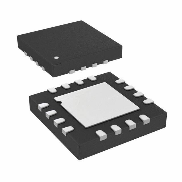
| 产品图片 |
|
| rohs | 符合RoHS无铅 / 符合限制有害物质指令(RoHS)规范要求 |
| 产品系列 | 放大器 IC,运算放大器 - 运放,Texas Instruments OPA2336PAG4MicroAmplifier™ |
| 数据手册 | |
| 产品型号 | OPA2336PAG4 |
| PCN组件/产地 | |
| 产品种类 | 运算放大器 - 运放 |
| 供应商器件封装 | 8-PDIP |
| 共模抑制比—最小值 | 76 dB |
| 关闭 | No Shutdown |
| 包装 | 管件 |
| 单位重量 | 523.200 mg |
| 压摆率 | 0.03 V/µs |
| 商标 | Texas Instruments |
| 增益带宽生成 | 0.1 MHz |
| 增益带宽积 | 100kHz |
| 安装类型 | 通孔 |
| 安装风格 | Through Hole |
| 封装 | Tube |
| 封装/外壳 | 8-DIP(0.300",7.62mm) |
| 封装/箱体 | PDIP-8 |
| 工作温度 | -40°C ~ 85°C |
| 工作电源电压 | 2.3 V to 5.5 V |
| 工厂包装数量 | 50 |
| 技术 | CMOS |
| 放大器类型 | Low Offset Voltage Amplifier |
| 最大工作温度 | + 85 C |
| 最小工作温度 | - 40 C |
| 标准包装 | 50 |
| 电压-电源,单/双 (±) | 2.3 V ~ 5.5 V |
| 电压-输入失调 | 60µV |
| 电流-电源 | 20µA |
| 电流-输入偏置 | 1pA |
| 电流-输出/通道 | 5mA |
| 电源电流 | 0.064 mA |
| 电路数 | 2 |
| 系列 | OPA2336 |
| 设计资源 | http://www.digikey.com/product-highlights/cn/zh/texas-instruments-webench-design-center/3176 |
| 转换速度 | 0.03 V/us |
| 输入偏压电流—最大 | 10 pA |
| 输入参考电压噪声 | 40 nV |
| 输入补偿电压 | 500 uV |
| 输出类型 | 满摆幅 |
| 通道数量 | 2 Channel |


- 商务部:美国ITC正式对集成电路等产品启动337调查
- 曝三星4nm工艺存在良率问题 高通将骁龙8 Gen1或转产台积电
- 太阳诱电将投资9.5亿元在常州建新厂生产MLCC 预计2023年完工
- 英特尔发布欧洲新工厂建设计划 深化IDM 2.0 战略
- 台积电先进制程称霸业界 有大客户加持明年业绩稳了
- 达到5530亿美元!SIA预计今年全球半导体销售额将创下新高
- 英特尔拟将自动驾驶子公司Mobileye上市 估值或超500亿美元
- 三星加码芯片和SET,合并消费电子和移动部门,撤换高东真等 CEO
- 三星电子宣布重大人事变动 还合并消费电子和移动部门
- 海关总署:前11个月进口集成电路产品价值2.52万亿元 增长14.8%


PDF Datasheet 数据手册内容提取
OPA336 OPA4336 OPA2336 OPA336 OPA2336 OPA4336 SBOS068C – JANUARY 1997 – REVISED JANUARY 2005 SINGLE-SUPPLY, Power micro CMOS OPERATIONAL AMPLIFIERS Amplifier Series micro ™ FEATURES DESCRIPTION (cid:1) SINGLE-SUPPLY OPERATION OPA336 series microPower CMOS operational amplifiers (cid:1) RAIL-TO-RAIL OUTPUT (within 3mV) are designed for battery-powered applications. They (cid:1) microPOWER: I = 20µA/Amplifier operate on a single supply with operation as low as 2.1V. Q The output is rail-to-rail and swings to within 3mV of the (cid:1) microSIZE PACKAGES supplies with a 100kΩ load. The common-mode range (cid:1) LOW OFFSET VOLTAGE: 125µV max extends to the negative supply—ideal for single-supply (cid:1) SPECIFIED FROM V = 2.3V to 5.5V applications. Single, dual, and quad versions have identical S specifications for maximum design flexibility. (cid:1) SINGLE, DUAL, AND QUAD VERSIONS In addition to small size and low quiescent current (20µA/amplifier), they feature low offset voltage APPLICATIONS (125µV max), low input bias current (1pA), and high open- loop gain (115dB). Dual and quad designs feature (cid:1) BATTERY-POWERED INSTRUMENTS completely independent circuitry for lowest crosstalk and (cid:1) PORTABLE DEVICES freedom from interaction. (cid:1) HIGH-IMPEDANCE APPLICATIONS OPA336 packages are the tiny SOT23-5 surface mount (cid:1) PHOTODIODE PRE-AMPS and SO-8 surface-mount. OPA2336 come in the miniature MSOP-8 surface-mount, SO-8 surface-mount, and DIP-8 (cid:1) PRECISION INTEGRATORS packages. The OPA4336 package is the space-saving (cid:1) MEDICAL INSTRUMENTS SSOP-16 surface-mount. All are specified from (cid:1) TEST EQUIPMENT –40°C to +85°C and operate from –55°C to +125°C. A macromodel is available for download (at www.ti.com) OPA336 for design analysis. Out 1 5 V+ OPA4336 V– 2 Out A 1 16 Out D +In 3 4 –In –In A 2 15 –In D A D SOT23-5 +In A 3 14 +In D OPA336 OPA2336 V+ 4 13 V– NC 1 8 NC Out A 1 8 V+ +In B 5 12 +In C A B C –In 2 7 V+ –In A 2 7 Out B –In B 6 11 –In C +In 3 6 Output +In A 3 B 6 –In B Out B 7 10 Out C V– 4 5 NC V– 4 5 +In B NC 8 9 NC SO-8 DIP-8, SO-8, MSOP-8 SSOP-16 NC = No Connection NC = No Connection Please be aware that an important notice concerning availability, standard warranty, and use in critical applications of Texas Instruments semiconductor products and disclaimers thereto appears at the end of this data sheet. All trademarks are the property of their respective owners. PRODUCTION DATA information is current as of publication date. Copyright © 1997-2005, Texas Instruments Incorporated Products conform to specifications per the terms of Texas Instruments standard warranty. Production processing does not necessarily include testing of all parameters. www.ti.com
PACKAGE/ORDERING INFORMATION(1) PACKAGE DRAWING PACKAGE PRODUCT PACKAGE-LEAD DESIGNATOR MARKING Single OPA336N SOT23-5 DBV A36(2) OPA336NA SOT23-5 DBV A36(2) OPA336NJ SOT23-5 DBV J36 OPA336U SO-8 Surface-Mount D OPA336U OPA336UA SO-8 Surface-Mount D OPA336UA OPA336UJ SO-8 Surface-Mount D OPA336UJ Dual OPA2336E MSOP-8 Surface-Mount DGK B36(2) OPA2336EA MSOP-8 Surface-Mount DGK B36(2) OPA2336P DIP-8 P OPA2336P OPA2336PA DIP-8 P OPA2336PA OPA2336U SO-8 Surface-Mount D OPA2336U OPA2336UA SO-8 Surface-Mount D OPA2336UA Quad OPA4336EA SSOP-16 Surface-Mount DBQ OPA4336EA NOTES: (1) For the most current package and ordering information, see the package option addendum at the end of this data sheet. (2) Grade will be marked on the Reel. ABSOLUTE MAXIMUM RATINGS(1) ELECTROSTATIC Supply Voltage...................................................................................7.5V DISCHARGE SENSITIVITY Signal Input Terminals, Voltage(2).....................(V–) –0.3V to (V+) +0.3V Current(2)....................................................10mA This integrated circuit can be damaged by ESD. Texas Output Short-Circuit(3)..............................................................Continuous Operating Temperature..................................................–55°C to +125°C Instruments recommends that all integrated circuits be handled Storage Temperature.....................................................–55°C to +125°C with appropriate precautions. Failure to observe proper han- Junction Temperature......................................................................150°C dling and installation procedures can cause damage. Lead Temperature (soldering, 10s).................................................300°C ESD Rating: ESD damage can range from subtle performance degrada- Charged Device Model, OPA336 NJ and UJ only (CDM)(4).......1000V tion to complete device failure. Precision integrated circuits Human Body Model (HBM)(4).........................................................500V Machine Model (MM)(4)..................................................................100V may be more susceptible to damage because very small parametric changes could cause the device not to meet its NOTES: (1) Stresses above these ratings may cause permanent damage. Exposure to absolute maximum conditions for extended periods may published specifications. degrade device reliability. These are stress ratings only. Functional opera- tion of the device at these conditions, or beyond the specified operating conditions, is not implied. (2) Input terminals are diode-clamped to the power supply rails. Input signals that can swing more than 0.3V beyond the supply rails should be current-limited to 10mA or less. (3) Short-circuit to ground, one amplifier per package. (4) OPA336 NJ and UJ have been tested to CDM of 1000V. All other previous package versions have been tested using HBM and MM. Results are shown. OPA336, 2336, 4336 2 www.ti.com SBOS068C
ELECTRICAL CHARACTERISTICS: V = 2.3V to 5.5V S ° ° Boldface limits apply over the specified temperature range, T = –40 C to +85 C. A At T = +25°C, V = +5V, and R = 25kΩ connected to V /2, unless otherwise noted. A S L S OPA336NA, UA OPA336N, U OPA2336EA, PA, UA OPA2336E, P, U OPA4336EA OPA336NJ, UJ PARAMETER CONDITION MIN TYP(1) MAX MIN TYP MAX MIN TYP MAX UNITS OFFSET VOLTAGE Input Offset Voltage V ±60 ±125 ✻ ±500 ±500 ±2500 µV OS vs Temperature dV /dT ±1.5 ✻ ✻ µV/°C OS vs Power Supply PSRR V = 2.3V to 5.5V 25 100 ✻ ✻ ✻ ✻ ✻ µV/V S Over Temperature V = 2.3V to 5.5V 130 ✻ ✻ ✻ µV/V S Channel Separation, dc 0.1 ✻ ✻ µV/V INPUT BIAS CURRENT Input Bias Current I ±1 ±10 ✻ ✻ ✻ ✻ pA B Over Temperature ±60 ✻ ✻ pA Input Offset Current I ±1 ±10 ✻ ✻ ✻ ✻ pA OS NOISE Input Voltage Noise, f = 0.1 to 10Hz 3 ✻ ✻ µVp-p Input Voltage Noise Density, f = 1kHze 40 ✻ ✻ nV/√Hz n Current Noise Density, f = 1kHz i 30 ✻ ✻ fA/√Hz n INPUT VOLTAGE RANGE Common-Mode Voltage Range V –0.2 (V+) –1 ✻ ✻ ✻ ✻ V CM Common-Mode Rejection Ratio CMRR –0.2V < V < (V+) –1V 80 90 76 86 76 86 dB CM Over Temperature –0.2V < V < (V+) –1V 76 74 74 dB CM INPUT IMPEDANCE Differential 1013 || 2 ✻ ✻ Ω || pF Common-Mode 1013 || 4 ✻ ✻ Ω || pF OPEN-LOOP GAIN Open-Loop Voltage Gain A R = 25kΩ, 100mV < V < (V+) – 100mV 100 115 90 ✻ 90 ✻ dB OL L O Over Temperature R = 25kΩ, 100mV < V < (V+) – 100mV 100 90 90 dB L O R = 5kΩ, 500mV < V < (V+) – 500mV 90 106 ✻ ✻ ✻ ✻ dB L O Over Temperature R = 5kΩ, 500mV < V < (V+) – 500mV 90 ✻ ✻ dB L O FREQUENCY RESPONSE Gain-Bandwidth Product GBW V = 5V, G = 1 100 ✻ ✻ kHz S Slew Rate SR V = 5V, G = 1 0.03 ✻ ✻ V/µs S Overload Recovery Time V • G = V 100 ✻ ✻ µs IN S OUTPUT Voltage Output Swing from Rail(2) R = 100kΩ, A ≥ 70dB 3 ✻ ✻ mV L OL R = 25kΩ, A ≥ 90dB 20 100 ✻ ✻ ✻ ✻ mV L OL Over Temperature R = 25kΩ, A ≥ 90dB 100 ✻ ✻ mV L OL R = 5kΩ, A ≥ 90dB 70 500 ✻ ✻ ✻ ✻ mV L OL Over Temperature R = 5kΩ, A ≥ 90dB 500 ✻ ✻ mV L OL Short-Circuit Current I ±5 ✻ ✻ mA SC Capacitive Load Drive C See Text ✻ ✻ pF LOAD POWER SUPPLY Specified Voltage Range V 2.3 5.5 ✻ ✻ ✻ ✻ V S Minimum Operating Voltage 2.1 ✻ ✻ V Quiescent Current (per amplifier) I I = 0 20 32 ✻ ✻ 23 38 µA Q O Over Temperature I = 0 36 ✻ 42 µA O TEMPERATURE RANGE Specified Range –40 +85 ✻ ✻ ✻ ✻ °C Operating Range –55 +125 ✻ ✻ ✻ ✻ °C Storage Range –55 +125 ✻ ✻ ✻ ✻ °C Thermal Resistance θ JA SOT-23-5 Surface-Mount 200 ✻ ✻ °C/W MSOP-8 Surface-Mount 150 ✻ °C/W SO-8 Surface-Mount 150 ✻ ✻ °C/W DIP-8 100 ✻ °C/W SSOP-16 Surface-Mount 100 ✻ °C/W DIP-14 80 ✻ °C/W ✻ Specifications same as OPA2336E, P, U. NOTES: (1) V = +5V. (2) Output voltage swings are measured between the output and positive and negative power-supply rails. S OPA336, 2336, 4336 3 SBOS068C www.ti.com
TYPICAL CHARACTERISTICS At T = +25°C, V = +5V, and R = 25kΩ connected to V /2, unless otherwise noted. A S L S POWER-SUPPLY and COMMON-MODE OPEN-LOOP GAIN/PHASE vs FREQUENCY REJECTION RATIO vs FREQUENCY 100 100 CMRR G 80 0 80 B) 60 –45 B) age Gain (d 40 Φ –90 Phase (°) R, CMRR (d 6400 PSRR Volt 20 –135 PSR 20 0 –180 –20 0 1 10 100 1k 10k 100k 1M 1 10 100 1k 10k 100k Frequency (Hz) Frequency (Hz) QUIESCENT CURRENT vs SUPPLY VOLTAGE QUIESCENT CURRENT vs TEMPERATURE 30 30 Per Amplifier Per Amplifier V = +5V 25 S A) 25 A) µ µ nt ( nt ( 20 e e urr urr C 20 C 15 nt nt e e c c s s 10 V = +2.3V e e S Qui 15 Qui 5 10 0 2.0 2.5 3.0 3.5 4.0 4.5 5.0 5.5 6.0 –75 –50 –25 0 25 50 75 100 125 Supply Voltage (V) Temperature (°C) SHORT-CIRCUIT CURRENT vs SUPPLY VOLTAGE SHORT-CIRCUIT CURRENT vs TEMPERATURE ±6 8 7 ±5 V = +5V A) A) S m m 6 ent ( ±4 +ISC ent ( 5 –ISC urr urr Circuit C ±±32 Circuit C 43 +ISC +ISC hort- –ISC hort- 2 VS = +2.3V –ISC S ±1 S 1 0 0 2.0 2.5 3.0 3.5 4.0 4.5 5.0 5.5 6.0 –75 –50 –25 0 25 50 75 100 125 Supply Voltage (V) Temperature (°C) OPA336, 2336, 4336 4 www.ti.com SBOS068C
TYPICAL CHARACTERISTICS (Cont.) At T = +25°C, V = +5V, and R = 25kΩ connected to V /2, unless otherwise noted. A S L S INPUT VOLTAGE AND CURRENT NOISE SPECTRAL DENSITY vs FREQUENCY CHANNEL SEPARATION vs FREQUENCY 1k 1k 150 Voltage Noise √V/Hz) 100 100 √A/Hz) on (dB) 140 oise (n oise (f eparati 130 N N S Voltage 10 10 Current Channel 120 Dchuaanl naenlsd. QQuuaadd mdeeaviscuerse,d Gc h=an n1e, l aAll to D or B to C—other combinations Current Noise yield improved rejection. 1 110 1 10 100 1k 10k 100k 100 1k 10k 100k Frequency (Hz) Frequency (Hz) MAXIMUM OUTPUT VOLTAGE vs FREQUENCY A , CMRR, PSRR vs TEMPERATURE OL 6 120 A OL 5 VS = +5.5V 110 Vp-p) 4 R (dB) oltage ( 3 R, PSR 100 PSRR V V = +2.3V R 90 put 2 S CM CMRR Out , OL A 80 1 0 70 100 1k 10k 100k –75 –50 –25 0 25 50 75 100 125 Frequency (Hz) Temperature (°C) OFFSET VOLTAGE OFFSET VOLTAGE DRIFT MAGNITUDE PRODUCTION DISTRIBUTION PRODUCTION DISTRIBUTION 25 25 Typical production Typical production distribution of distribution of %) 20 packaged units. %) 20 packaged units. s ( s ( plifier 15 plifier 15 m m A A of 10 of 10 nt nt e e c c Per 5 Per 5 0.1% 0.3% 0.2% 0.1% 0 0 0 0 0 0 0 0 0 0 0 0 0 5 5 5 1 5 5 5 2 5 5 5 3 5 5 5 4 –50 –40 –30 –20 –10 10 20 30 40 50 0.2 0. 0.7 1.2 1. 1.7 2.2 2. 2.7 3.2 3. 3.7 Offset Voltage (µV) Offset Voltage Drift (µV/°C) OPA336, 2336, 4336 5 SBOS068C www.ti.com
TYPICAL CHARACTERISTICS (Cont.) At T = +25°C, V = +5V, and R = 25kΩ connected to V /2, unless otherwise noted. A S L S INPUT BIAS CURRENT INPUT BIAS CURRENT vs TEMPERATURE vs INPUT COMMON-MODE VOLTAGE 1k 4 A) 100 A) 3 p p nt ( nt ( VS = +5V e e Curr 10 Curr 2 s s a a Bi Bi ut ut p 1 p 1 n n I I 0.1 0 –75 –50 –25 0 25 50 75 100 125 0 1 2 3 4 5 Temperature (°C) Common-Mode Voltage (V) OUTPUT VOLTAGE SWING vs OUTPUT CURRENT OUTPUT VOLTAGE SWING vs OUTPUT CURRENT 5 –2.5 V = ±2.5V V = +5V S S 4 –2.0 V) SCouurrrceinntg –55°C +25°C +125°C V) CSiunrkreinngt ge ( 3 ge ( –1.5 a a Volt VS = +2.3V Volt +125°C ut 2 +125°C ut –1.0 p p ut ut O –55°C O –55°C 1 –0.5 +25°C +25°C 0 0 0 1 2 3 4 5 6 7 8 –0 –1 –2 –3 –4 –5 –6 –7 –8 Output Current (mA) Output Current (mA) SMALL-SIGNAL STEP RESPONSE LARGE-SIGNAL STEP RESPONSE G = 1, C = 200pF, V = +5V G = 1, C = 620pF, V = +5V L S L S v V/div mV/di m 0 0 0 2 5 50µs/div 200µs/div OPA336, 2336, 4336 6 www.ti.com SBOS068C
APPLICATIONS INFORMATION Normally, input bias current is approximately 1pA. How- ever, input voltages exceeding the power supplies can OPA336 series op amps are fabricated on a state-of-the-art cause excessive current to flow in or out of the input pins. 0.6 micron CMOS process. They are unity-gain stable and Momentary voltages greater than the power supply can be suitable for a wide range of general-purpose applications. tolerated as long as the current on the input pins is limited Power-supply pins should be bypassed with 0.01µF ceramic to 10mA. This is easily accomplished with an input resis- capacitors. OPA336 series op amps are protected against tor, as shown in Figure 2. reverse battery voltages. OPERATING VOLTAGE +5V OPA336 series op amps can operate from a +2.1V to +5.5V I single supply with excellent performance. Most behavior OVERLOAD 10mA max remains unchanged throughout the full operating voltage OPAx336 VOUT V range. Parameters which vary significantly with operating IN 5kΩ voltage are shown in the typical characteristics. OPA336 series op amps are fully specified for operation from +2.3V FIGURE 2. Input Current Protection for Voltages Exceeding to +5.5V; a single limit applies over the supply range. In the Supply Voltage. addition, many parameters are ensured over the specified temperature range, –40°C to +85°C. CAPACITIVE LOAD AND STABILITY OPA336 series op amps can drive a wide range of capaci- INPUT VOLTAGE tive loads. However, all op amps under certain conditions The input common-mode range of OPA336 series op amps may become unstable. Op-amp configuration, gain, and extends from (V–) – 0.2V to (V+) – 1V. For normal load value are just a few of the factors to consider when operation, inputs should be limited to this range. The determining stability. absolute maximum input voltage is 300mV beyond the When properly configured, OPA336 series op amps can supplies. Thus, inputs greater than the input drive approximately 10,000pF. An op amp in unity-gain common-mode range but less than maximum input volt- configuration is the most vulnerable to capacitive load. The age, while not valid, will not cause any damage to the op capacitive load reacts with the op amp’s output resistance, amp. Furthermore, the inputs may go beyond the power along with any additional load resistance, to create a pole in supplies without phase inversion, as shown in Figure 1, the response which degrades the phase margin. In unity gain, unlike some other op amps. OPA336 series op amps perform well with a pure capacitive load up to about 300pF. Increasing gain enhances the amplifier’s ability to drive loads beyond this level. One method of improving capacitive load drive in the unity-gain configuration is to insert a 50Ω to 100Ω resistor 6V inside the feedback loop, as shown in Figure 3. This reduces ringing with large capacitive loads while maintaining DC V OUT R S 100Ω OPAx336 V OUT 0V V IN C R L L FIGURE 1. No Phase Inversion with Inputs Greater than the Power-Supply Voltage. FIGURE 3. Series Resistor in Unity-Gain Configuration Improves Capacitive Load Drive. OPA336, 2336, 4336 7 SBOS068C www.ti.com
accuracy. For example, with R = 25kΩ, OPA336 series op Direct Current (DC) error at the output; however, this error L amps perform well with capacitive loads in excess of 1000pF, may be insignificant. For instance, with R = 100kΩ and L as shown in Figure 4. Without R , capacitive load drive is R = 100Ω, there is only about a 0.1% error at the output. S S typically 350pF for these conditions, as shown in Figure 5. Figure 5 shows the recommended operating regions for the OPA336. Decreasing the load resistance generally improves capacitive load drive. Figure 5 also illustrates how stability R = 100Ω, Load = 2kΩ || 1000pF, V = +5V differs depending on where the resistive load is connected. S S With G = +1 and R = 10kΩ connected to V /2, the OPA336 L S can typically drive 500pF. Connecting the same load to ground improves capacitive load drive to 1000pF. v di V/ m 10k 0 2 Operation Above Selected Gain Curve Not Recommended pF) G = +1 R Gto =G r+o2und ad ( RL to Ground L o 50µs/div e L 1k v citi FIGURE 4. Small-Signal Step Response Using Series Re- pa a sistor to Improve Capacitive Load Drive. C G = +1 Alternatively, the resistor may be connected in series with RL to VS/2 VS = +5V, VO = VS/2 100 the output outside of the feedback loop. However, if there is 5 10 100 a resistive load parallel to the capacitive load, it and the Resistive Load (kΩ) series resistor create a voltage divider. This introduces a FIGURE 5. Stability—Capacitive Load vs Resistive Load. OPA336, 2336, 4336 8 www.ti.com SBOS068C
PACKAGE OPTION ADDENDUM www.ti.com 6-Feb-2020 PACKAGING INFORMATION Orderable Device Status Package Type Package Pins Package Eco Plan Lead/Ball Finish MSL Peak Temp Op Temp (°C) Device Marking Samples (1) Drawing Qty (2) (6) (3) (4/5) HPA00779NA/3K ACTIVE SOT-23 DBV 5 3000 Green (RoHS NIPDAU Level-1-260C-UNLIM A36 & no Sb/Br) OPA2336E/250 ACTIVE VSSOP DGK 8 250 Green (RoHS NIPDAUAG Level-2-260C-1 YEAR -40 to 85 B36 & no Sb/Br) OPA2336E/2K5 ACTIVE VSSOP DGK 8 2500 Green (RoHS NIPDAUAG Level-2-260C-1 YEAR -40 to 85 B36 & no Sb/Br) OPA2336E/2K5G4 ACTIVE VSSOP DGK 8 2500 Green (RoHS NIPDAUAG Level-2-260C-1 YEAR -40 to 85 B36 & no Sb/Br) OPA2336EA/250 ACTIVE VSSOP DGK 8 250 Green (RoHS NIPDAUAG Level-2-260C-1 YEAR -40 to 85 B36 & no Sb/Br) OPA2336EA/250G4 ACTIVE VSSOP DGK 8 250 Green (RoHS NIPDAUAG Level-2-260C-1 YEAR -40 to 85 B36 & no Sb/Br) OPA2336EA/2K5 ACTIVE VSSOP DGK 8 2500 Green (RoHS NIPDAUAG Level-2-260C-1 YEAR -40 to 85 B36 & no Sb/Br) OPA2336P ACTIVE PDIP P 8 50 Green (RoHS NIPDAU N / A for Pkg Type -40 to 85 OPA2336P & no Sb/Br) OPA2336PA ACTIVE PDIP P 8 50 Green (RoHS NIPDAU N / A for Pkg Type -40 to 85 OPA2336P & no Sb/Br) A OPA2336U ACTIVE SOIC D 8 75 Green (RoHS NIPDAU Level-2-260C-1 YEAR -40 to 85 OPA & no Sb/Br) 2336U OPA2336U/2K5 ACTIVE SOIC D 8 2500 Green (RoHS NIPDAU Level-2-260C-1 YEAR -40 to 85 OPA & no Sb/Br) 2336U OPA2336U/2K5G4 ACTIVE SOIC D 8 2500 Green (RoHS NIPDAU Level-2-260C-1 YEAR -40 to 85 OPA & no Sb/Br) 2336U OPA2336UA ACTIVE SOIC D 8 75 Green (RoHS NIPDAU Level-2-260C-1 YEAR -40 to 85 OPA & no Sb/Br) 2336U A OPA2336UA/2K5 ACTIVE SOIC D 8 2500 Green (RoHS NIPDAU Level-2-260C-1 YEAR -40 to 85 OPA & no Sb/Br) 2336U A OPA2336UA/2K5G4 ACTIVE SOIC D 8 2500 Green (RoHS NIPDAU Level-2-260C-1 YEAR -40 to 85 OPA & no Sb/Br) 2336U A OPA2336UG4 ACTIVE SOIC D 8 75 Green (RoHS NIPDAU Level-2-260C-1 YEAR -40 to 85 OPA & no Sb/Br) 2336U Addendum-Page 1
PACKAGE OPTION ADDENDUM www.ti.com 6-Feb-2020 Orderable Device Status Package Type Package Pins Package Eco Plan Lead/Ball Finish MSL Peak Temp Op Temp (°C) Device Marking Samples (1) Drawing Qty (2) (6) (3) (4/5) OPA336N/250 ACTIVE SOT-23 DBV 5 250 Green (RoHS NIPDAU Level-1-260C-UNLIM A36 & no Sb/Br) OPA336N/250G4 ACTIVE SOT-23 DBV 5 250 Green (RoHS NIPDAU Level-1-260C-UNLIM A36 & no Sb/Br) OPA336N/3K ACTIVE SOT-23 DBV 5 3000 Green (RoHS NIPDAU Level-1-260C-UNLIM A36 & no Sb/Br) OPA336N/3KG4 ACTIVE SOT-23 DBV 5 3000 Green (RoHS NIPDAU Level-1-260C-UNLIM A36 & no Sb/Br) OPA336NA/250 ACTIVE SOT-23 DBV 5 250 Green (RoHS NIPDAU Level-1-260C-UNLIM A36 & no Sb/Br) OPA336NA/250G4 ACTIVE SOT-23 DBV 5 250 Green (RoHS NIPDAU Level-1-260C-UNLIM A36 & no Sb/Br) OPA336NA/3K ACTIVE SOT-23 DBV 5 3000 Green (RoHS NIPDAU Level-1-260C-UNLIM A36 & no Sb/Br) OPA336NA/3KG4 ACTIVE SOT-23 DBV 5 3000 Green (RoHS NIPDAU Level-1-260C-UNLIM A36 & no Sb/Br) OPA336NJ/250 ACTIVE SOT-23 DBV 5 250 Green (RoHS NIPDAU Level-1-260C-UNLIM -40 to 85 J36 & no Sb/Br) OPA336NJ/3K ACTIVE SOT-23 DBV 5 3000 Green (RoHS NIPDAU Level-1-260C-UNLIM -40 to 85 J36 & no Sb/Br) OPA336NJ/3KG4 ACTIVE SOT-23 DBV 5 3000 Green (RoHS NIPDAU Level-1-260C-UNLIM -40 to 85 J36 & no Sb/Br) OPA336U ACTIVE SOIC D 8 75 Green (RoHS NIPDAU Level-2-260C-1 YEAR OPA & no Sb/Br) 336U OPA336U/2K5 ACTIVE SOIC D 8 2500 Green (RoHS NIPDAU Level-2-260C-1 YEAR OPA & no Sb/Br) 336U OPA336UA ACTIVE SOIC D 8 75 Green (RoHS NIPDAU Level-2-260C-1 YEAR OPA & no Sb/Br) 336U A OPA336UA/2K5 ACTIVE SOIC D 8 2500 Green (RoHS NIPDAU Level-2-260C-1 YEAR OPA & no Sb/Br) 336U A OPA4336EA/250 ACTIVE SSOP DBQ 16 250 Green (RoHS NIPDAU Level-2-260C-1 YEAR -40 to 85 OPA & no Sb/Br) 4336EA OPA4336EA/250G4 ACTIVE SSOP DBQ 16 250 Green (RoHS NIPDAU Level-2-260C-1 YEAR -40 to 85 OPA & no Sb/Br) 4336EA Addendum-Page 2
PACKAGE OPTION ADDENDUM www.ti.com 6-Feb-2020 Orderable Device Status Package Type Package Pins Package Eco Plan Lead/Ball Finish MSL Peak Temp Op Temp (°C) Device Marking Samples (1) Drawing Qty (2) (6) (3) (4/5) OPA4336EA/2K5 ACTIVE SSOP DBQ 16 2500 Green (RoHS NIPDAU Level-2-260C-1 YEAR -40 to 85 OPA & no Sb/Br) 4336EA OPA4336EA/2K5G4 ACTIVE SSOP DBQ 16 2500 Green (RoHS NIPDAU Level-2-260C-1 YEAR -40 to 85 OPA & no Sb/Br) 4336EA (1) The marketing status values are defined as follows: ACTIVE: Product device recommended for new designs. LIFEBUY: TI has announced that the device will be discontinued, and a lifetime-buy period is in effect. NRND: Not recommended for new designs. Device is in production to support existing customers, but TI does not recommend using this part in a new design. PREVIEW: Device has been announced but is not in production. Samples may or may not be available. OBSOLETE: TI has discontinued the production of the device. (2) RoHS: TI defines "RoHS" to mean semiconductor products that are compliant with the current EU RoHS requirements for all 10 RoHS substances, including the requirement that RoHS substance do not exceed 0.1% by weight in homogeneous materials. Where designed to be soldered at high temperatures, "RoHS" products are suitable for use in specified lead-free processes. TI may reference these types of products as "Pb-Free". RoHS Exempt: TI defines "RoHS Exempt" to mean products that contain lead but are compliant with EU RoHS pursuant to a specific EU RoHS exemption. Green: TI defines "Green" to mean the content of Chlorine (Cl) and Bromine (Br) based flame retardants meet JS709B low halogen requirements of <=1000ppm threshold. Antimony trioxide based flame retardants must also meet the <=1000ppm threshold requirement. (3) MSL, Peak Temp. - The Moisture Sensitivity Level rating according to the JEDEC industry standard classifications, and peak solder temperature. (4) There may be additional marking, which relates to the logo, the lot trace code information, or the environmental category on the device. (5) Multiple Device Markings will be inside parentheses. Only one Device Marking contained in parentheses and separated by a "~" will appear on a device. If a line is indented then it is a continuation of the previous line and the two combined represent the entire Device Marking for that device. (6) Lead/Ball Finish - Orderable Devices may have multiple material finish options. Finish options are separated by a vertical ruled line. Lead/Ball Finish values may wrap to two lines if the finish value exceeds the maximum column width. Important Information and Disclaimer:The information provided on this page represents TI's knowledge and belief as of the date that it is provided. TI bases its knowledge and belief on information provided by third parties, and makes no representation or warranty as to the accuracy of such information. Efforts are underway to better integrate information from third parties. TI has taken and continues to take reasonable steps to provide representative and accurate information but may not have conducted destructive testing or chemical analysis on incoming materials and chemicals. TI and TI suppliers consider certain information to be proprietary, and thus CAS numbers and other limited information may not be available for release. In no event shall TI's liability arising out of such information exceed the total purchase price of the TI part(s) at issue in this document sold by TI to Customer on an annual basis. OTHER QUALIFIED VERSIONS OF OPA336 : Addendum-Page 3
PACKAGE OPTION ADDENDUM www.ti.com 6-Feb-2020 •Enhanced Product: OPA336-EP NOTE: Qualified Version Definitions: •Enhanced Product - Supports Defense, Aerospace and Medical Applications Addendum-Page 4
PACKAGE MATERIALS INFORMATION www.ti.com 24-Apr-2020 TAPE AND REEL INFORMATION *Alldimensionsarenominal Device Package Package Pins SPQ Reel Reel A0 B0 K0 P1 W Pin1 Type Drawing Diameter Width (mm) (mm) (mm) (mm) (mm) Quadrant (mm) W1(mm) OPA2336E/250 VSSOP DGK 8 250 180.0 12.4 5.3 3.4 1.4 8.0 12.0 Q1 OPA2336E/2K5 VSSOP DGK 8 2500 330.0 12.4 5.3 3.4 1.4 8.0 12.0 Q1 OPA2336EA/250 VSSOP DGK 8 250 180.0 12.4 5.3 3.4 1.4 8.0 12.0 Q1 OPA2336EA/2K5 VSSOP DGK 8 2500 330.0 12.4 5.3 3.4 1.4 8.0 12.0 Q1 OPA2336U/2K5 SOIC D 8 2500 330.0 12.4 6.4 5.2 2.1 8.0 12.0 Q1 OPA2336UA/2K5 SOIC D 8 2500 330.0 12.4 6.4 5.2 2.1 8.0 12.0 Q1 OPA336N/250 SOT-23 DBV 5 250 178.0 9.0 3.3 3.2 1.4 4.0 8.0 Q3 OPA336N/3K SOT-23 DBV 5 3000 178.0 9.0 3.23 3.17 1.37 4.0 8.0 Q3 OPA336N/3K SOT-23 DBV 5 3000 179.0 8.4 3.2 3.2 1.4 4.0 8.0 Q3 OPA336NA/250 SOT-23 DBV 5 250 178.0 9.0 3.3 3.2 1.4 4.0 8.0 Q3 OPA336NA/3K SOT-23 DBV 5 3000 178.0 9.0 3.3 3.2 1.4 4.0 8.0 Q3 OPA336NA/3K SOT-23 DBV 5 3000 179.0 8.4 3.2 3.2 1.4 4.0 8.0 Q3 OPA336NJ/250 SOT-23 DBV 5 250 178.0 9.0 3.23 3.17 1.37 4.0 8.0 Q3 OPA336NJ/3K SOT-23 DBV 5 3000 178.0 9.0 3.3 3.2 1.4 4.0 8.0 Q3 OPA336NJ/3K SOT-23 DBV 5 3000 179.0 8.4 3.2 3.2 1.4 4.0 8.0 Q3 OPA336U/2K5 SOIC D 8 2500 330.0 12.4 6.4 5.2 2.1 8.0 12.0 Q1 OPA336UA/2K5 SOIC D 8 2500 330.0 12.4 6.4 5.2 2.1 8.0 12.0 Q1 OPA4336EA/250 SSOP DBQ 16 250 180.0 12.4 6.4 5.2 2.1 8.0 12.0 Q1 PackMaterials-Page1
PACKAGE MATERIALS INFORMATION www.ti.com 24-Apr-2020 Device Package Package Pins SPQ Reel Reel A0 B0 K0 P1 W Pin1 Type Drawing Diameter Width (mm) (mm) (mm) (mm) (mm) Quadrant (mm) W1(mm) OPA4336EA/2K5 SSOP DBQ 16 2500 330.0 12.4 6.4 5.2 2.1 8.0 12.0 Q1 *Alldimensionsarenominal Device PackageType PackageDrawing Pins SPQ Length(mm) Width(mm) Height(mm) OPA2336E/250 VSSOP DGK 8 250 210.0 185.0 35.0 OPA2336E/2K5 VSSOP DGK 8 2500 367.0 367.0 35.0 OPA2336EA/250 VSSOP DGK 8 250 210.0 185.0 35.0 OPA2336EA/2K5 VSSOP DGK 8 2500 367.0 367.0 35.0 OPA2336U/2K5 SOIC D 8 2500 367.0 367.0 35.0 OPA2336UA/2K5 SOIC D 8 2500 367.0 367.0 35.0 OPA336N/250 SOT-23 DBV 5 250 180.0 180.0 18.0 OPA336N/3K SOT-23 DBV 5 3000 180.0 180.0 18.0 OPA336N/3K SOT-23 DBV 5 3000 203.0 203.0 35.0 OPA336NA/250 SOT-23 DBV 5 250 180.0 180.0 18.0 OPA336NA/3K SOT-23 DBV 5 3000 180.0 180.0 18.0 OPA336NA/3K SOT-23 DBV 5 3000 203.0 203.0 35.0 OPA336NJ/250 SOT-23 DBV 5 250 180.0 180.0 18.0 OPA336NJ/3K SOT-23 DBV 5 3000 180.0 180.0 18.0 OPA336NJ/3K SOT-23 DBV 5 3000 203.0 203.0 35.0 OPA336U/2K5 SOIC D 8 2500 367.0 367.0 35.0 PackMaterials-Page2
PACKAGE MATERIALS INFORMATION www.ti.com 24-Apr-2020 Device PackageType PackageDrawing Pins SPQ Length(mm) Width(mm) Height(mm) OPA336UA/2K5 SOIC D 8 2500 367.0 367.0 35.0 OPA4336EA/250 SSOP DBQ 16 250 210.0 185.0 35.0 OPA4336EA/2K5 SSOP DBQ 16 2500 367.0 367.0 35.0 PackMaterials-Page3
PACKAGE OUTLINE DBV0005A SOT-23 - 1.45 mm max height SCALE 4.000 SMALL OUTLINE TRANSISTOR C 3.0 2.6 0.1 C 1.75 1.45 1.45 B A 0.90 PIN 1 INDEX AREA 1 5 2X 0.95 3.05 2.75 1.9 1.9 2 4 3 0.5 5X 0.3 0.15 0.2 C A B (1.1) TYP 0.00 0.25 GAGE PLANE 0.22 TYP 0.08 8 TYP 0.6 0 0.3 TYP SEATING PLANE 4214839/E 09/2019 NOTES: 1. All linear dimensions are in millimeters. Any dimensions in parenthesis are for reference only. Dimensioning and tolerancing per ASME Y14.5M. 2. This drawing is subject to change without notice. 3. Refernce JEDEC MO-178. 4. Body dimensions do not include mold flash, protrusions, or gate burrs. Mold flash, protrusions, or gate burrs shall not exceed 0.15 mm per side. www.ti.com
EXAMPLE BOARD LAYOUT DBV0005A SOT-23 - 1.45 mm max height SMALL OUTLINE TRANSISTOR PKG 5X (1.1) 1 5 5X (0.6) SYMM (1.9) 2 2X (0.95) 3 4 (R0.05) TYP (2.6) LAND PATTERN EXAMPLE EXPOSED METAL SHOWN SCALE:15X SOLDER MASK SOLDER MASK METAL UNDER METAL OPENING OPENING SOLDER MASK EXPOSED METAL EXPOSED METAL 0.07 MAX 0.07 MIN ARROUND ARROUND NON SOLDER MASK SOLDER MASK DEFINED DEFINED (PREFERRED) SOLDER MASK DETAILS 4214839/E 09/2019 NOTES: (continued) 5. Publication IPC-7351 may have alternate designs. 6. Solder mask tolerances between and around signal pads can vary based on board fabrication site. www.ti.com
EXAMPLE STENCIL DESIGN DBV0005A SOT-23 - 1.45 mm max height SMALL OUTLINE TRANSISTOR PKG 5X (1.1) 1 5 5X (0.6) SYMM 2 (1.9) 2X(0.95) 3 4 (R0.05) TYP (2.6) SOLDER PASTE EXAMPLE BASED ON 0.125 mm THICK STENCIL SCALE:15X 4214839/E 09/2019 NOTES: (continued) 7. Laser cutting apertures with trapezoidal walls and rounded corners may offer better paste release. IPC-7525 may have alternate design recommendations. 8. Board assembly site may have different recommendations for stencil design. www.ti.com
PACKAGE OUTLINE D0008A SOIC - 1.75 mm max height SCALE 2.800 SMALL OUTLINE INTEGRATED CIRCUIT C SEATING PLANE .228-.244 TYP [5.80-6.19] .004 [0.1] C A PIN 1 ID AREA 6X .050 [1.27] 8 1 2X .189-.197 [4.81-5.00] .150 NOTE 3 [3.81] 4X (0 -15 ) 4 5 8X .012-.020 B .150-.157 [0.31-0.51] .069 MAX [3.81-3.98] .010 [0.25] C A B [1.75] NOTE 4 .005-.010 TYP [0.13-0.25] 4X (0 -15 ) SEE DETAIL A .010 [0.25] .004-.010 0 - 8 [0.11-0.25] .016-.050 [0.41-1.27] DETAIL A (.041) TYPICAL [1.04] 4214825/C 02/2019 NOTES: 1. Linear dimensions are in inches [millimeters]. Dimensions in parenthesis are for reference only. Controlling dimensions are in inches. Dimensioning and tolerancing per ASME Y14.5M. 2. This drawing is subject to change without notice. 3. This dimension does not include mold flash, protrusions, or gate burrs. Mold flash, protrusions, or gate burrs shall not exceed .006 [0.15] per side. 4. This dimension does not include interlead flash. 5. Reference JEDEC registration MS-012, variation AA. www.ti.com
EXAMPLE BOARD LAYOUT D0008A SOIC - 1.75 mm max height SMALL OUTLINE INTEGRATED CIRCUIT 8X (.061 ) [1.55] SYMM SEE DETAILS 1 8 8X (.024) [0.6] SYMM (R.002 ) TYP [0.05] 5 4 6X (.050 ) [1.27] (.213) [5.4] LAND PATTERN EXAMPLE EXPOSED METAL SHOWN SCALE:8X SOLDER MASK SOLDER MASK METAL OPENING OPENING METAL UNDER SOLDER MASK EXPOSED METAL EXPOSED METAL .0028 MAX .0028 MIN [0.07] [0.07] ALL AROUND ALL AROUND NON SOLDER MASK SOLDER MASK DEFINED DEFINED SOLDER MASK DETAILS 4214825/C 02/2019 NOTES: (continued) 6. Publication IPC-7351 may have alternate designs. 7. Solder mask tolerances between and around signal pads can vary based on board fabrication site. www.ti.com
EXAMPLE STENCIL DESIGN D0008A SOIC - 1.75 mm max height SMALL OUTLINE INTEGRATED CIRCUIT 8X (.061 ) [1.55] SYMM 1 8 8X (.024) [0.6] SYMM (R.002 ) TYP [0.05] 5 4 6X (.050 ) [1.27] (.213) [5.4] SOLDER PASTE EXAMPLE BASED ON .005 INCH [0.125 MM] THICK STENCIL SCALE:8X 4214825/C 02/2019 NOTES: (continued) 8. Laser cutting apertures with trapezoidal walls and rounded corners may offer better paste release. IPC-7525 may have alternate design recommendations. 9. Board assembly site may have different recommendations for stencil design. www.ti.com
None
PACKAGE OUTLINE DBQ0016A SSOP - 1.75 mm max height SCALE 2.800 SHRINK SMALL-OUTLINE PACKAGE C SEATING PLANE .228-.244 TYP [5.80-6.19] .004 [0.1] C A PIN 1 ID AREA 14X .0250 [0.635] 16 1 2X .189-.197 .175 [4.81-5.00] [4.45] NOTE 3 8 9 16X .008-.012 B .150-.157 [0.21-0.30] .069 MAX [3.81-3.98] [1.75] NOTE 4 .007 [0.17] C A B .005-.010 TYP [0.13-0.25] SEE DETAIL A .010 [0.25] GAGE PLANE .004-.010 0 - 8 [0.11-0.25] .016-.035 [0.41-0.88] DETAIL A (.041 ) TYPICAL [1.04] 4214846/A 03/2014 NOTES: 1. Linear dimensions are in inches [millimeters]. Dimensions in parenthesis are for reference only. Controlling dimensions are in inches. Dimensioning and tolerancing per ASME Y14.5M. 2. This drawing is subject to change without notice. 3. This dimension does not include mold flash, protrusions, or gate burrs. Mold flash, protrusions, or gate burrs shall not exceed .006 inch, per side. 4. This dimension does not include interlead flash. 5. Reference JEDEC registration MO-137, variation AB. www.ti.com
EXAMPLE BOARD LAYOUT DBQ0016A SSOP - 1.75 mm max height SHRINK SMALL-OUTLINE PACKAGE 16X (.063) [1.6] SYMM SEE DETAILS 1 16 16X (.016 ) [0.41] 14X (.0250 ) [0.635] 8 9 (.213) [5.4] LAND PATTERN EXAMPLE SCALE:8X SOLDER MASK SOLDER MASK METAL OPENING OPENING METAL .002 MAX .002 MIN [0.05] [0.05] ALL AROUND ALL AROUND NON SOLDER MASK SOLDER MASK DEFINED DEFINED SOLDER MASK DETAILS 4214846/A 03/2014 NOTES: (continued) 6. Publication IPC-7351 may have alternate designs. 7. Solder mask tolerances between and around signal pads can vary based on board fabrication site. www.ti.com
EXAMPLE STENCIL DESIGN DBQ0016A SSOP - 1.75 mm max height SHRINK SMALL-OUTLINE PACKAGE 16X (.063) [1.6] SYMM 1 16 16X (.016 ) [0.41] SYMM 14X (.0250 ) [0.635] 8 9 (.213) [5.4] SOLDER PASTE EXAMPLE BASED ON .005 INCH [0.127 MM] THICK STENCIL SCALE:8X 4214846/A 03/2014 NOTES: (continued) 8. Laser cutting apertures with trapezoidal walls and rounded corners may offer better paste release. IPC-7525 may have alternate design recommendations. 9. Board assembly site may have different recommendations for stencil design. www.ti.com
None
None
None
IMPORTANTNOTICEANDDISCLAIMER TI PROVIDES TECHNICAL AND RELIABILITY DATA (INCLUDING DATASHEETS), DESIGN RESOURCES (INCLUDING REFERENCE DESIGNS), APPLICATION OR OTHER DESIGN ADVICE, WEB TOOLS, SAFETY INFORMATION, AND OTHER RESOURCES “AS IS” AND WITH ALL FAULTS, AND DISCLAIMS ALL WARRANTIES, EXPRESS AND IMPLIED, INCLUDING WITHOUT LIMITATION ANY IMPLIED WARRANTIES OF MERCHANTABILITY, FITNESS FOR A PARTICULAR PURPOSE OR NON-INFRINGEMENT OF THIRD PARTY INTELLECTUAL PROPERTY RIGHTS. These resources are intended for skilled developers designing with TI products. You are solely responsible for (1) selecting the appropriate TI products for your application, (2) designing, validating and testing your application, and (3) ensuring your application meets applicable standards, and any other safety, security, or other requirements. These resources are subject to change without notice. TI grants you permission to use these resources only for development of an application that uses the TI products described in the resource. Other reproduction and display of these resources is prohibited. No license is granted to any other TI intellectual property right or to any third party intellectual property right. TI disclaims responsibility for, and you will fully indemnify TI and its representatives against, any claims, damages, costs, losses, and liabilities arising out of your use of these resources. TI’s products are provided subject to TI’s Terms of Sale (www.ti.com/legal/termsofsale.html) or other applicable terms available either on ti.com or provided in conjunction with such TI products. TI’s provision of these resources does not expand or otherwise alter TI’s applicable warranties or warranty disclaimers for TI products. Mailing Address: Texas Instruments, Post Office Box 655303, Dallas, Texas 75265 Copyright © 2020, Texas Instruments Incorporated