ICGOO在线商城 > 集成电路(IC) > 线性 - 放大器 - 仪表,运算放大器,缓冲器放大器 > ONET4201PARGTR
 Datasheet下载
- 型号: ONET4201PARGTR
- 制造商: Texas Instruments
- 库位|库存: xxxx|xxxx
- 要求:
| 数量阶梯 | 香港交货 | 国内含税 |
| +xxxx | $xxxx | ¥xxxx |
查看当月历史价格
查看今年历史价格
ONET4201PARGTR产品简介:
ICGOO电子元器件商城为您提供ONET4201PARGTR由Texas Instruments设计生产,在icgoo商城现货销售,并且可以通过原厂、代理商等渠道进行代购。 ONET4201PARGTR价格参考。Texas InstrumentsONET4201PARGTR封装/规格:线性 - 放大器 - 仪表,运算放大器,缓冲器放大器, 限制 放大器 1 电路 差分 16-QFN(3x3)。您可以下载ONET4201PARGTR参考资料、Datasheet数据手册功能说明书,资料中有ONET4201PARGTR 详细功能的应用电路图电压和使用方法及教程。
Texas Instruments(德州仪器)的ONET4201PARGTR是一款应用于高速光通信系统的集成电路,属于线性放大器类别中的限幅后置放大器(Limiting Post-Amplifier),常用于光纤通信接收端。其主要功能是对来自光电探测器的微弱信号进行放大和整形,以提供稳定的数字输出信号。

该器件广泛应用于以下场景:

1. 光纤通信系统:如1G到10Gbps的SFP(小型可插拔)光模块、XFP模块等,适用于短距离和中距离的数据传输。
2. 电信设备:包括接入网设备、以太网交换机、路由器等需要高速光信号处理的通信设备。
3. 数据中心与服务器网络接口:支持高速数据传输,满足高带宽需求。
4. 工业与测试设备:用于光信号的检测与处理,如光时域反射仪(OTDR)、光功率计等。

ONET4201PARGTR具备低功耗、高灵敏度、宽输入动态范围等特点,适合在复杂电磁环境中稳定工作,是构建高性能光通信链路的重要组件。
| 参数 | 数值 |
| -3db带宽 | 25kHz |
| 产品目录 | 集成电路 (IC) |
| 描述 | IC OPAMP LIMITING 25KHZ 16QFN |
| 产品分类 | Linear - Amplifiers - Instrumentation, OP Amps, Buffer Amps |
| 品牌 | Texas Instruments |
| 数据手册 | |
| 产品图片 |
|
| 产品型号 | ONET4201PARGTR |
| rohs | 无铅 / 符合限制有害物质指令(RoHS)规范要求 |
| 产品系列 | - |
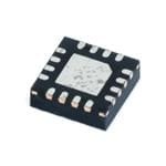
| 供应商器件封装 | 16-QFN(3x3) |
| 其它名称 | 296-19279-6 |
| 包装 | Digi-Reel® |
| 压摆率 | - |
| 增益带宽积 | - |
| 安装类型 | 表面贴装 |
| 封装/外壳 | 16-VFQFN 裸露焊盘 |
| 工作温度 | -40°C ~ 85°C |
| 放大器类型 | 限制 |
| 标准包装 | 1 |
| 电压-电源,单/双 (±) | 3 V ~ 3.6 V |
| 电压-输入失调 | - |
| 电流-电源 | 35mA |
| 电流-输入偏置 | - |
| 电流-输出/通道 | - |
| 电路数 | 1 |
| 输出类型 | 差分 |

.jpg)


PDF Datasheet 数据手册内容提取
ONET4201PA www.ti.com SLLS652–NOVEMBER2005 155 Mbps to 4.25 Gbps Limiting Amplifier With LOS and RSSI FEATURES DESCRIPTION • Multi-RateOperationfrom155Mbpsupto The ONET4201PA is a versatile high-speed, 3.3-V 4.25Gbps limiting amplifier for multiple fiber optic applications • 89mWPowerConsumption withdataratesupto4.25Gbps. • InputOffsetCancellation This device provides a gain of about 50 dB, which • HighInputDynamicRange ensures a fully differential output swing for input signalsaslowas3mV . • OutputDisable p-p • CMLDataOutputs The high input signal dynamic range ensures low jitter output signals even when overdriven with input • ReceiveSignalStrengthIndicator(RSSI) signalswingsashighas1200mV . p-p • LossofSignalDetection The ONET4201PA provides a loss of signal detection • PolaritySelect aswellasareceivedsignalstrengthindicator. • Single3.3-VSupply The part is available in a small footprint 3-mm · • SurfaceMountSmallFootprint3-mm· 3-mm 3-mm16-pinQFNpackageandispin-compatiblewith 16-PinQFNPackage theONET2501PAandONET3301PA. • Pin-CompatiblewiththeONET2501PAand This power efficient limiting amplifier typically ONET3301PA dissipates less than 89 mW and it is characterized for operationfrom–40(cid:176) Cto85(cid:176) C. APPLICATIONS • Multi-RateOC3toOC-48FECSONET/SDH TransmissionSystems • 1.0625Gbps,2.125Gbps,and4.25GbpsFibre ChannelReceivers • GigabitEthernetReceivers Pleasebeawarethatanimportantnoticeconcerningavailability,standardwarranty,anduseincriticalapplicationsofTexas Instrumentssemiconductorproductsanddisclaimerstheretoappearsattheendofthisdatasheet. PRODUCTIONDATAinformationiscurrentasofpublicationdate. Copyright©2005,TexasInstrumentsIncorporated Products conform to specifications per the terms of the Texas Instruments standard warranty. Production processing does not necessarilyincludetestingofallparameters.
ONET4201PA www.ti.com SLLS652–NOVEMBER2005 BLOCK DIAGRAM AsimplifiedblockdiagramoftheONET4201PAisshowninFigure1. This compact, low power 4.25 Gbps limiting amplifier consists of a high-speed data path with offset cancellation block, a loss of signal and RSSI detection block, and a bandgap voltage reference and bias current generation block. COC2 COC1 VCC GND Offset Cancellation OUTPOL DIN+ + + + + + DOUT+ DIN− − − − − − DOUT− Input Buffer Gain Stage Gain Stage Gain Stage CML Output Buffer DISABLE BRanedfegraepn cVeo altnadge Loss aonf dSignal LOS Bias Current RSSI Detection RSSI Generation TH B0052-01 Figure1.SimplifiedBlockDiagramoftheONET4201PA HIGH SPEED DATA PATH The high-speed data signal is applied to the data path by means of the input signal pins DIN+/DIN–. The data path consists of the input stage with 2 · 50-W on-chip line termination to VCC, three gain stages, which provide the required typical gain of about 50 dB, and a CML output stage. The amplified data output signal is available at theoutputpinsDOUT+/DOUT–,whichprovide2· 50-W back-terminationtoVCC.Theoutputstagealso includes a data polarity switching function, which is controlled by the OUTPOL input, and a disable function, controlled by thesignalappliedtotheDISABLEinputpin. Offset cancellation compensates for internal offset voltages and thus ensures proper operation even for very smallinputdatasignals. Thelowfrequencycutoffistypicallyaslowas25kHzwiththebuilt-infiltercapacitor. For applications which require even lower cutoff frequencies, an additional external filter capacitor may be connectedtotheCOC1/COC2pins. LOSS OF SIGNAL AND RSSI DETECTION Theoutputsignaloftheinputbufferismonitored by the loss of signal and RSSI detection circuitry. In this block a signal is generated that is linearly proportional to the input amplitude over a wide input voltage range. This signal isavailableattheRSSIoutputpin. Furthermore, this circuit block compares the input signal to a threshold which can be programmed by means of anexternalresistorconnectedtotheTHpin.Iftheinputsignalfallsbelowthespecifiedthreshold, a loss of signal isindicatedattheLOSpin. The relation between the LOS assert voltage V (in mV ) and the external resistor R (in kW ) connected to AST p-p TH theTHpincanbeapproximatedasgivenbelow: 2
ONET4201PA www.ti.com SLLS652–NOVEMBER2005 RTH(cid:3) 20.8k(cid:1) (cid:1)300(cid:1) (cid:5)VAST(cid:4)mVp(cid:2)p(cid:2)1(cid:6) (1) 20.8mV p(cid:2)p V (cid:3) (cid:1)1mV AST R (cid:4)k(cid:1)(cid:2)0.3 p(cid:2)p TH (2) BANDGAP VOLTAGE AND BIAS GENERATION The ONET4201PA limiting amplifier is supplied by a single 3.3-V– 10% supply voltage connected to the VCC pins.Thisvoltageisreferredtoground(GND). An on-chip bandgap voltage circuit generates a supply voltage independent reference from which all other internallyrequiredvoltagesandbiascurrentsarederived. PACKAGE For the ONET4201PA a small footprint 3-mm · 3-mm 16-pin QFN package, with a lead pitch of 0,5 mm, is used. ThepinoutisshowninFigure2. RGT PACKAGE (TOP VIEW) 2 1 D C C SI N O O S G C C R 16 15 14 13 VCC 1 12 VCC DIN+ 2 11 DOUT+ EP DIN− 3 10 DOUT− VCC 4 9 OUTPOL 5 6 7 8 H E S D T L O N B L G A S DI P0019-01 Figure2.PinoutofONET4201PAina3mmx3mm16PinQFNPackage(TopView) TERMINALFUNCTIONS TERMINAL TYPE DESCRIPTION NO. NAME 1,4,12 VCC supply 3.3-V– 10%supplyvoltage 2 DIN+ analog-in Non-inverteddatainput.On-chip50-W terminatedtoVCC. 3 DIN– analog-in Inverteddatainput.On-chip50-W terminatedtoVCC. 5 TH analog-in LOSthresholdadjustmentwithresistortoGND. 6 DISABLE CMOS-in DisablesCMLoutputstagewhensettohighlevel. 7 LOS CMOS-out Highlevelindicatesthattheinputsignalamplitudeisbelowtheprogrammedthresholdlevel. 8,16,EP GND supply Circuitground.Exposeddiepad(EP)mustbegrounded. Outputdatasignalpolarityselect(internallypulledhigh).Settingtoahighlevelorleavingthepin 9 OUTPOL CMOS-in openselectsnormalpolarity.Lowlevelselectsinvertedpolarity. 10 DOUT– CML-out Inverteddataoutput.On-chip50-W back-terminatedtoVCC. 11 DOUT+ CML-out Non-inverteddataoutput.On-chip50-W back-terminatedtoVCC. 3
ONET4201PA www.ti.com SLLS652–NOVEMBER2005 TERMINALFUNCTIONS(continued) TERMINAL TYPE DESCRIPTION NO. NAME Analogoutputvoltageproportionaltotheinputdataamplitude.Indicatesthestrengthofthe 13 RSSI analog-out receivedsignal(RSSI). Offsetcancellationfiltercapacitorterminal1.Connectanadditionalfiltercapacitorbetweenthispin 14 COC1 analog andCOC2(pin15). TodisabletheoffsetcancellationloopconnectCOC1andCOC2(pins14and15). Offsetcancellationfiltercapacitorterminal2.Connectanadditionalfiltercapacitorbetweenthispin 15 COC2 analog andCOC1(pin14). TodisabletheoffsetcancellationloopconnectCOC1andCOC2(pins14and15). ABSOLUTE MAXIMUM RATINGS overoperatingfree-airtemperaturerange(unlessotherwisenoted)(1) VALUE/UNIT V Supplyvoltage (2) –0.3Vto4.0V CC V ,V VoltageatDIN+,DIN–(2) 0.5Vto4.0V DIN+ DIN- V ,V ,V ,V ,V , VoltageatTH,DISABLE,LOS,OUTPOL,DOUT+,DOUT-,RSSI, –0.3Vto4.0V TH DISABLE LOS OUTPOL DOUT+ V ,V ,V ,V COC1,COC2 (2) DOUT– RSSI COC1 COC2 V DifferentialvoltagebetweenCOC1andCOC2 ±1V COC,DIFF V DifferentialvoltagebetweenDIN+andDIN– ±2.5V DIN,DIFF I CurrentintoLOS -1to9mA LOS I ,I ,I ,I Continuouscurrentatinputsandoutputs –25mAto25mA DIN+ DIN– DOUT+ DOUT– ESD ESDratingatallpins 2kV(HBM) T Maximumjunctiontemperature 125°C J(max) T Storagetemperaturerange –65to85°C STG T Characterizedfree-airoperatingtemperaturerange –40to85°C A T Leadtemperature1,6mm(1/16inch)fromcasefor10seconds 260°C LEAD (1) Stressesbeyondthoselistedunder“absolutemaximumratings”maycausepermanentdamagetothedevice.Thesearestressratings only,andfunctionaloperationofthedeviceattheseoranyotherconditionsbeyondthoseindicatedunder“recommendedoperating conditions”isnotimplied.Exposuretoabsolute-maximum-ratedconditionsforextendedperiodsmayaffectdevicereliability. (2) Allvoltagevaluesarewithrespecttonetworkgroundterminal. RECOMMENDED OPERATING CONDITIONS MIN TYP MAX UNIT V Supplyvoltage 3 3.3 3.6 V CC T Operatingfree-airtemperature –40 85 (cid:176) C A V CMOSinputhighvoltage 2.1 V IH V CMOSinputlowvoltage 0.6 V IL 4
ONET4201PA www.ti.com SLLS652–NOVEMBER2005 DC ELECTRICAL CHARACTERISTICS overrecommendedoperatingconditions(unlessotherwisenoted) PARAMETER TESTCONDITIONS MIN TYP MAX UNIT V Supplyvoltage 3 3.3 3.6 V CC DISABLE=low(includesCMLoutputcurrent) 35 45 I Supplycurrent mA VCC DISABLE=low(excludesCMLoutputcurrent) 27 35 DISABLE=high 0.25 10 V Differentialdataoutputvoltageswing mV OD DISABLE=low,5mV £ V £ 1200mV 520 760 1200 p-p p-p IN p-p R ,R Datainput/outputresistance Single-ended 50 W IN OUT Input=8mV ,R ‡ 10kW 200 p-p RSSI RSSIoutputvoltage mV Input=80mV ,R ‡ 10kW 1900 p-p RSSI RSSIlinearity 8mV £ V £ 80mV – 3% p-p IN p-p V Datainputsensitivity BER<10–10 3 5 mV IN(MIN) p-p V Datainputoverload 1200 mV IN(MAX) p-p LOShighvoltage I =30µA 2.4 V SOURCE LOSlowvoltage I =1mA 0.4 V SINK AC ELECTRICAL CHARACTERISTICS overrecommendedoperatingconditions,typicaloperatingconditionisatV =3.3VandT =25(cid:176) C(unlessotherwisenoted) CC A PARAMETER TESTCONDITIONS MIN TYP MAX UNIT C =open 25 OC Lowfrequency–3dBbandwidth kHz C =0.54µF 0.8 OC Datarate 4.25 Gb/s v Inputreferrednoise 230 µV NI RMS K28.5patternat4.25Gbps 3 19 DJ Deterministicjitter K28.5patternat2.125Gbps 4 35 ps p-p K28.5patternat1.0625Gbps 4 72 Input=5mVpp 9 RJ Randomjitter ps RMS Input=10mVpp 4 t Outputrisetime 20%to80% 45 85 ps R t Outputfalltime 20%to80% 45 85 ps F LOShysteresis K28.5patternat4.25Gbps,20log(V /V ) 2.5 4.5 dB DEA AST R LOSthresholdadjustmentresistor See (1) 1.2 6.8 kW TH range R =2.5kW ,K28.5patternat4.25Gbps(1) 10 TH V LOSassertvoltage mV AST R =6.8kW ,K28.5patternat4.25Gbps(1) 2 5 p-p TH R =2.5kW ,K28.5patternat4.25Gbps(1) 17 TH V LOSde-assertvoltage mV DEA R =6.8kW ,K28.5patternat4.25Gbps(1) 8 20 p-p TH T LOSassert/deasserttime 2 100 µs LOS T Disableresponsetime 20 ns DIS (1) ForagivenexternalresistorconnectedtotheTHpintheLOSassertvoltagevaluemayvaryduetopart-to-partvariations.Ifhigh precisionisrequired,adjustmentofthisresistorforeachdeviceismandatory. 5
ONET4201PA www.ti.com SLLS652–NOVEMBER2005 TYPICAL CHARACTERISTICS TypicaloperatingconditionisatV =3.3VandT =25(cid:176) C(unlessotherwisenoted). CC A TRANSFERFUNCTION RANDOMJITTER vsINPUTAMPLITUDE 800 14 P-P 700 12 V m − 600 ge S 10 a M olt 500 sR V p Output 400 Jitter − 8 al m 6 nti 300 do e n Differ 200 Ra 4 − D 2 O 100 V 0 0 0 1 2 3 4 5 6 0 5 10 15 20 25 30 35 40 VID − Differential Input Voltage − mVP-P VID − Differential Input Voltage − mVP-P G001 G002 Figure3. Figure4. BIT-ERRORRATIO FREQUENCYRESPONSE INPUTAMPLITUDE 100 60 55 10-2 50 10-4 45 B 10-6 − d 40 Ratio 10-8 Gain 35 or al 30 Bit Err 1100--1102 mall Sign 2205 S 15 10-14 10 10-16 5 10-18 0 1 2 3 4 5 6 7 0.01 0.1 1 10 VID − Differential Input Voltage − mVP-P f − Frequency − GHz G003 G004 Figure5. Figure6. 6
ONET4201PA www.ti.com SLLS652–NOVEMBER2005 TYPICAL CHARACTERISTICS (continued) TypicaloperatingconditionisatV =3.3VandT =25(cid:176) C(unlessotherwisenoted). CC A OUTPUTEYE-DIAGRAMAT4.25GBPS OUTPUTEYE-DIAGRAMAT4.25GBPS ANDMINIMUMINPUTVOLTAGE(5mV ) ANDMAXIMUMINPUTVOLTAGE(1200mV ) p-p p-p v v Di Di V/ V/ m m 0 0 6 6 1 1 − − e e g g a a olt olt V V ut ut p p ut ut O O al al nti nti e e er er Diff Diff − − D D O O V V t − Time − 50 ps/Div t − Time − 50 ps/Div G005 G006 Figure7. Figure8. OUTPUTEYE-DIAGRAMAT4.25GBPSAND85(cid:176) C ANDMINIMUMINPUTVOLTAGE(5mV ) p-p v Di V/ m 0 6 1 − e g a olt V ut p ut O al nti e er Diff − D O V t − Time − 50 ps/Div G007 Figure9. 7
ONET4201PA www.ti.com SLLS652–NOVEMBER2005 TYPICAL CHARACTERISTICS (continued) TypicaloperatingconditionisatV =3.3VandT =25(cid:176) C(unlessotherwisenoted). CC A OUTPUTEYE-DIAGRAMAT2.125GBPS OUTPUTEYE-DIAGRAMAT2.125GBPS ANDMINIMUMINPUTVOLTAGE(5mV ) ANDMAXIMUMINPUTVOLTAGE(1200mV ) p-p p-p v v Di Di V/ V/ m m 0 0 6 6 1 1 − − e e g g a a olt olt V V ut ut p p ut ut O O al al nti nti e e er er Diff Diff − − D D O O V V t − Time − 100 ps/Div t − Time − 100 ps/Div G008 G009 Figure10. Figure11. OUTPUTEYE-DIAGRAMAT1.0625GBPS OUTPUTEYE-DIAGRAMAT1.0625GBPS ANDMINIMUMINPUTVOLTAGE(5mV ) ANDMAXIMUMINPUTVOLTAGE(1200mV ) p-p p-p v v Di Di V/ V/ m m 0 0 6 6 1 1 − − e e g g a a olt olt V V ut ut p p ut ut O O al al nti nti e e er er Diff Diff − − D D O O V V t − Time − 200 ps/Div t − Time − 200 ps/Div G010 G011 Figure12. Figure13. 8
ONET4201PA www.ti.com SLLS652–NOVEMBER2005 TYPICAL CHARACTERISTICS (continued) TypicaloperatingconditionisatV =3.3VandT =25(cid:176) C(unlessotherwisenoted). CC A ASSERT/DEASSERTVOLTAGE DIFFERENTIALINPUTRETURNGAIN vsTHRESHOLDRESISTANCE vsFREQUENCY 40 0 B −5 35 d P-P n − −10 mV 30 Gai −15 ge − urn −20 ert Volta 2205 nput Ret −−3205 Deass 15 LOS Deassert Voltage ential I −35 rt/ er −40 sse 10 Diff −45 OS A LOS Assert Voltage 11 − −50 L 5 D D S −55 0 −60 0 1 2 3 4 5 6 7 10 100 1k 10k Rth − Threshold Resistance − kW f − Frequency − MHz G012 G013 Figure14. Figure15. DIFFERENTIALOUTPUTRETURNGAIN RSSIVOLTAGE vsFREQUENCY vsINPUTAMPLITUDE 0 V m 2400 B −5 − − d ge 2200 ain −10 olta 2000 G V Return −−2105 dicator 11680000 put −25 h In 1400 ut −30 gt O n 1200 rential −−4305 als Stre 1000 e n 800 Diff −45 Sig − e 600 22 −50 eiv 400 D c SD −55 − Re 200 −6010 100 1k 10k SSI 0 R 0 10 20 30 40 50 60 70 80 90 100 f − Frequency − MHz G014 VID − Differential Input Voltage − mVP-P G015 Figure16. Figure17. 9
ONET4201PA www.ti.com SLLS652–NOVEMBER2005 APPLICATION INFORMATION Figure 18 shows the ONET4201PA connected with an ac-coupled interface to the data signal source as well as totheoutputload. Besides the ac-coupling capacitors C through C in the input and output data signal lines, the only required 1 4 external component is the LOS threshold setting resistor R . In addition, an optional external filter capacitor th (C )maybeusedifalowercutofffrequencyisdesired. OC COC Optional RSSI GND OC2 OC1 RSSI C C VCC VCC VCC C1 C3 DIN+ DIN+ DOUT+ DOUT+ ONET4201PA DIN− C2 DIN− 16-Pin QFN DOUT− C4 DOUT− VCC E OUTPOL OUTPOL L B A S D TH DIS LO GN DISABLE LOS RTH S0072-01 Figure18.BasicApplicationCircuitWithAC-CoupledI/Os 10
PACKAGE OPTION ADDENDUM www.ti.com 6-Feb-2020 PACKAGING INFORMATION Orderable Device Status Package Type Package Pins Package Eco Plan Lead/Ball Finish MSL Peak Temp Op Temp (°C) Device Marking Samples (1) Drawing Qty (2) (6) (3) (4/5) ONET4201PARGTR ACTIVE VQFN RGT 16 3000 Green (RoHS NIPDAU Level-2-260C-1 YEAR -40 to 85 401P & no Sb/Br) ONET4201PARGTRG4 ACTIVE VQFN RGT 16 3000 Green (RoHS NIPDAU Level-2-260C-1 YEAR -40 to 85 401P & no Sb/Br) ONET4201PARGTT ACTIVE VQFN RGT 16 250 Green (RoHS NIPDAU Level-2-260C-1 YEAR -40 to 85 401P & no Sb/Br) ONET4201PARGTTG4 ACTIVE VQFN RGT 16 250 Green (RoHS NIPDAU Level-2-260C-1 YEAR -40 to 85 401P & no Sb/Br) (1) The marketing status values are defined as follows: ACTIVE: Product device recommended for new designs. LIFEBUY: TI has announced that the device will be discontinued, and a lifetime-buy period is in effect. NRND: Not recommended for new designs. Device is in production to support existing customers, but TI does not recommend using this part in a new design. PREVIEW: Device has been announced but is not in production. Samples may or may not be available. OBSOLETE: TI has discontinued the production of the device. (2) RoHS: TI defines "RoHS" to mean semiconductor products that are compliant with the current EU RoHS requirements for all 10 RoHS substances, including the requirement that RoHS substance do not exceed 0.1% by weight in homogeneous materials. Where designed to be soldered at high temperatures, "RoHS" products are suitable for use in specified lead-free processes. TI may reference these types of products as "Pb-Free". RoHS Exempt: TI defines "RoHS Exempt" to mean products that contain lead but are compliant with EU RoHS pursuant to a specific EU RoHS exemption. Green: TI defines "Green" to mean the content of Chlorine (Cl) and Bromine (Br) based flame retardants meet JS709B low halogen requirements of <=1000ppm threshold. Antimony trioxide based flame retardants must also meet the <=1000ppm threshold requirement. (3) MSL, Peak Temp. - The Moisture Sensitivity Level rating according to the JEDEC industry standard classifications, and peak solder temperature. (4) There may be additional marking, which relates to the logo, the lot trace code information, or the environmental category on the device. (5) Multiple Device Markings will be inside parentheses. Only one Device Marking contained in parentheses and separated by a "~" will appear on a device. If a line is indented then it is a continuation of the previous line and the two combined represent the entire Device Marking for that device. (6) Lead/Ball Finish - Orderable Devices may have multiple material finish options. Finish options are separated by a vertical ruled line. Lead/Ball Finish values may wrap to two lines if the finish value exceeds the maximum column width. Important Information and Disclaimer:The information provided on this page represents TI's knowledge and belief as of the date that it is provided. TI bases its knowledge and belief on information provided by third parties, and makes no representation or warranty as to the accuracy of such information. Efforts are underway to better integrate information from third parties. TI has taken and Addendum-Page 1
PACKAGE OPTION ADDENDUM www.ti.com 6-Feb-2020 continues to take reasonable steps to provide representative and accurate information but may not have conducted destructive testing or chemical analysis on incoming materials and chemicals. TI and TI suppliers consider certain information to be proprietary, and thus CAS numbers and other limited information may not be available for release. In no event shall TI's liability arising out of such information exceed the total purchase price of the TI part(s) at issue in this document sold by TI to Customer on an annual basis. Addendum-Page 2
PACKAGE MATERIALS INFORMATION www.ti.com 12-Feb-2019 TAPE AND REEL INFORMATION *Alldimensionsarenominal Device Package Package Pins SPQ Reel Reel A0 B0 K0 P1 W Pin1 Type Drawing Diameter Width (mm) (mm) (mm) (mm) (mm) Quadrant (mm) W1(mm) ONET4201PARGTR VQFN RGT 16 3000 330.0 12.4 3.3 3.3 1.1 8.0 12.0 Q2 ONET4201PARGTT VQFN RGT 16 250 180.0 12.4 3.3 3.3 1.1 8.0 12.0 Q2 PackMaterials-Page1
PACKAGE MATERIALS INFORMATION www.ti.com 12-Feb-2019 *Alldimensionsarenominal Device PackageType PackageDrawing Pins SPQ Length(mm) Width(mm) Height(mm) ONET4201PARGTR VQFN RGT 16 3000 350.0 350.0 43.0 ONET4201PARGTT VQFN RGT 16 250 210.0 185.0 35.0 PackMaterials-Page2
None
PACKAGE OUTLINE RGT0016A VQFN - 1 mm max height SCALE 3.600 PLASTIC QUAD FLATPACK - NO LEAD A 3.1 B 2.9 PIN 1 INDEX AREA 3.1 2.9 1 MAX C SEATING PLANE 0.05 0.08 0.00 1.45 0.1 (0.2) TYP 5 8 EXPOSED THERMAL PAD 12X 0.5 4 9 4X 17 SYMM 1.5 1 12 0.30 16X 0.18 16 13 0.1 C A B PIN 1 ID SYMM (OPTIONAL) 0.05 0.5 16X 0.3 4219032/A 02/2017 NOTES: 1. All linear dimensions are in millimeters. Any dimensions in parenthesis are for reference only. Dimensioning and tolerancing per ASME Y14.5M. 2. This drawing is subject to change without notice. 3. The package thermal pad must be soldered to the printed circuit board for thermal and mechanical performance. 4. Reference JEDEC registration MO-220 www.ti.com
EXAMPLE BOARD LAYOUT RGT0016A VQFN - 1 mm max height PLASTIC QUAD FLATPACK - NO LEAD ( 1.45) SYMM 16 13 16X (0.6) 1 12 16X (0.24) 17 SYMM (0.475) (2.8) TYP 12X (0.5) 9 4 ( 0.2) TYP VIA 5 8 (R0.05) (0.475) TYP ALL PAD CORNERS (2.8) LAND PATTERN EXAMPLE EXPOSED METAL SHOWN SCALE:20X 0.07 MAX 0.07 MIN ALL AROUND ALL AROUND SOLDER MASK METAL OPENING EXPOSED METAL EXPOSED METAL SOLDER MASK METAL UNDER OPENING SOLDER MASK NON SOLDER MASK SOLDER MASK DEFINED DEFINED (PREFERRED) SOLDER MASK DETAILS 4219032/A 02/2017 NOTES: (continued) 5. This package is designed to be soldered to a thermal pad on the board. For more information, see Texas Instruments literature number SLUA271 (www.ti.com/lit/slua271). 6. Vias are optional depending on application, refer to device data sheet. If any vias are implemented, refer to their locations shown on this view. It is recommended that vias under paste be filled, plugged or tented. www.ti.com
EXAMPLE STENCIL DESIGN RGT0016A VQFN - 1 mm max height PLASTIC QUAD FLATPACK - NO LEAD ( 1.34) 16 13 16X (0.6) 1 12 16X (0.24) 17 SYMM (2.8) 12X (0.5) 9 4 METAL ALL AROUND 5 8 SYMM (R0.05) TYP (2.8) SOLDER PASTE EXAMPLE BASED ON 0.125 mm THICK STENCIL EXPOSED PAD 17: 86% PRINTED SOLDER COVERAGE BY AREA UNDER PACKAGE SCALE:25X 4219032/A 02/2017 NOTES: (continued) 7. Laser cutting apertures with trapezoidal walls and rounded corners may offer better paste release. IPC-7525 may have alternate design recommendations. www.ti.com
IMPORTANTNOTICEANDDISCLAIMER TI PROVIDES TECHNICAL AND RELIABILITY DATA (INCLUDING DATASHEETS), DESIGN RESOURCES (INCLUDING REFERENCE DESIGNS), APPLICATION OR OTHER DESIGN ADVICE, WEB TOOLS, SAFETY INFORMATION, AND OTHER RESOURCES “AS IS” AND WITH ALL FAULTS, AND DISCLAIMS ALL WARRANTIES, EXPRESS AND IMPLIED, INCLUDING WITHOUT LIMITATION ANY IMPLIED WARRANTIES OF MERCHANTABILITY, FITNESS FOR A PARTICULAR PURPOSE OR NON-INFRINGEMENT OF THIRD PARTY INTELLECTUAL PROPERTY RIGHTS. These resources are intended for skilled developers designing with TI products. You are solely responsible for (1) selecting the appropriate TI products for your application, (2) designing, validating and testing your application, and (3) ensuring your application meets applicable standards, and any other safety, security, or other requirements. These resources are subject to change without notice. TI grants you permission to use these resources only for development of an application that uses the TI products described in the resource. Other reproduction and display of these resources is prohibited. No license is granted to any other TI intellectual property right or to any third party intellectual property right. TI disclaims responsibility for, and you will fully indemnify TI and its representatives against, any claims, damages, costs, losses, and liabilities arising out of your use of these resources. TI’s products are provided subject to TI’s Terms of Sale (www.ti.com/legal/termsofsale.html) or other applicable terms available either on ti.com or provided in conjunction with such TI products. TI’s provision of these resources does not expand or otherwise alter TI’s applicable warranties or warranty disclaimers for TI products. Mailing Address: Texas Instruments, Post Office Box 655303, Dallas, Texas 75265 Copyright © 2020, Texas Instruments Incorporated