ICGOO在线商城 > 集成电路(IC) > 线性 - 放大器 - 仪表,运算放大器,缓冲器放大器 > AD711JR
 Datasheet下载
- 型号: AD711JR
- 制造商: Analog
- 库位|库存: xxxx|xxxx
- 要求:
| 数量阶梯 | 香港交货 | 国内含税 |
| +xxxx | $xxxx | ¥xxxx |
查看当月历史价格
查看今年历史价格
AD711JR产品简介:
ICGOO电子元器件商城为您提供AD711JR由Analog设计生产,在icgoo商城现货销售,并且可以通过原厂、代理商等渠道进行代购。 AD711JR价格参考¥8.94-¥8.94。AnalogAD711JR封装/规格:线性 - 放大器 - 仪表,运算放大器,缓冲器放大器, J-FET 放大器 1 电路 8-SOIC。您可以下载AD711JR参考资料、Datasheet数据手册功能说明书,资料中有AD711JR 详细功能的应用电路图电压和使用方法及教程。
AD711JR是由Analog Devices Inc.(亚德诺半导体公司)生产的一款高性能、低功耗的仪表放大器。它属于线性放大器系列,主要用于精密测量和信号调理应用中。以下是AD711JR的主要应用场景:

 1. 工业自动化与控制
   AD711JR在工业自动化领域有着广泛的应用,特别是在需要高精度传感器信号放大的场合。例如,在温度、压力、位移等传感器的信号调理电路中,AD711JR可以提供稳定的增益和低噪声性能,确保信号的准确传输。它还适用于电机控制系统中的电流和电压检测,帮助实现精确的闭环控制。

 2. 医疗设备
   在医疗电子设备中,如心电图(ECG)、脑电图(EEG)等生物医学信号采集系统,AD711JR能够有效放大微弱的生物电信号,同时保持极低的噪声水平。其高共模抑制比(CMRR)特性使得它能够在存在较大共模干扰的环境中稳定工作,确保测量结果的准确性。

 3. 测试与测量仪器
   AD711JR常用于各种高精度测试仪器中,如示波器、万用表等。它能够放大来自探头或其他传感器的微弱信号,确保测量结果的精度和可靠性。此外,AD711JR的低功耗特性使其适合便携式或电池供电的测试设备,延长了设备的工作时间。

 4. 音频处理
   在音频设备中,AD711JR可用于前置放大器,放大来自麦克风或其他音频源的微弱信号。它的低失真和低噪声特性有助于提高音频质量,特别适用于专业级音频设备和高保真音响系统。

 5. 数据采集系统
   在数据采集系统中,AD711JR可以作为前端信号调理模块,放大来自传感器的模拟信号,并将其传递给模数转换器(ADC)。其宽工作温度范围和良好的稳定性使其适合在恶劣环境下使用,如户外环境监测系统或工业现场的数据采集。

 总结
AD711JR凭借其高精度、低噪声、低功耗以及优异的共模抑制能力,广泛应用于工业、医疗、测试测量、音频处理和数据采集等领域。它能够有效提升系统的测量精度和可靠性,尤其适用于需要处理微弱信号的场合。
| 参数 | 数值 |
| -3db带宽 | 4MHz |
| 产品目录 | 集成电路 (IC)半导体 |
| 描述 | IC OPAMP JFET 4MHZ 8SOIC精密放大器 PREC HIGH Spd BIFET |
| 产品分类 | Linear - Amplifiers - Instrumentation, OP Amps, Buffer Amps集成电路 - IC |
| 品牌 | Analog Devices |
| 产品手册 | |
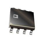
| 产品图片 |
|
| rohs | 否不符合限制有害物质指令(RoHS)规范要求 |
| 产品系列 | 放大器 IC,精密放大器,Analog Devices AD711JR- |
| 数据手册 | |
| 产品型号 | AD711JR |
| PCN过时产品 | |
| 产品培训模块 | http://www.digikey.cn/PTM/IndividualPTM.page?site=cn&lang=zhs&ptm=12927http://www.digikey.cn/PTM/IndividualPTM.page?site=cn&lang=zhs&ptm=30008http://www.digikey.cn/PTM/IndividualPTM.page?site=cn&lang=zhs&ptm=26202 |
| 产品种类 | 精密放大器 |
| 供应商器件封装 | 8-SOIC |
| 共模抑制比—最小值 | 88 dB |
| 关闭 | No |
| 包装 | 管件 |
| 压摆率 | 20 V/µs |
| 双重电源电压 | +/- 15 V |
| 商标 | Analog Devices |
| 增益带宽生成 | 4 MHz |
| 增益带宽积 | - |
| 安装类型 | 表面贴装 |
| 安装风格 | SMD/SMT |
| 封装 | Tube |
| 封装/外壳 | 8-SOIC(0.154",3.90mm 宽) |
| 封装/箱体 | SOIC-8 |
| 工作温度 | 0°C ~ 70°C |
| 工作电源电压 | 9 V to 36 V |
| 工厂包装数量 | 98 |
| 放大器类型 | J-FET |
| 最大功率耗散 | 500 mW |
| 最大双重电源电压 | +/- 18 V |
| 最大工作温度 | + 85 C |
| 最小双重电源电压 | +/- 4.5 V |
| 最小工作温度 | - 40 C |
| 标准包装 | 98 |
| 电压-电源,单/双 (±) | 9 V ~ 36 V, ±4.5 V ~ 18 V |
| 电压-输入失调 | 300µV |
| 电压增益dB | 112.04 dB |
| 电流-电源 | 2.5mA |
| 电流-输入偏置 | 15pA |
| 电流-输出/通道 | 25mA |
| 电源电压-最大 | 36 V |
| 电源电压-最小 | 9 V |
| 电源电流 | 2.8 mA |
| 电源类型 | Dual |
| 电路数 | 1 |
| 系列 | AD711 |
| 视频文件 | http://www.digikey.cn/classic/video.aspx?PlayerID=1364138032001&width=640&height=505&videoID=2245193153001http://www.digikey.cn/classic/video.aspx?PlayerID=1364138032001&width=640&height=505&videoID=2245193159001 |
| 转换速度 | 20 V/us at +/- 15 V |
| 输入偏压电流—最大 | 50 pA |
| 输入补偿电压 | 300 uV |
| 输出类型 | No |
| 通道数量 | 1 Channel |


- 商务部:美国ITC正式对集成电路等产品启动337调查
- 曝三星4nm工艺存在良率问题 高通将骁龙8 Gen1或转产台积电
- 太阳诱电将投资9.5亿元在常州建新厂生产MLCC 预计2023年完工
- 英特尔发布欧洲新工厂建设计划 深化IDM 2.0 战略
- 台积电先进制程称霸业界 有大客户加持明年业绩稳了
- 达到5530亿美元!SIA预计今年全球半导体销售额将创下新高
- 英特尔拟将自动驾驶子公司Mobileye上市 估值或超500亿美元
- 三星加码芯片和SET,合并消费电子和移动部门,撤换高东真等 CEO
- 三星电子宣布重大人事变动 还合并消费电子和移动部门
- 海关总署:前11个月进口集成电路产品价值2.52万亿元 增长14.8%


PDF Datasheet 数据手册内容提取
a Precision, Low Cost, High Speed, BiFET Op Amp AD711 FEATURES CONNECTION DIAGRAMS Enhanced Replacement for LF411 and TL081 AC PERFORMANCE NC S16e tVtl/e(cid:2)ss t om (cid:1)in0 S.0le1w% Rina 1te.0 ( A(cid:2)Ds711J) OFNFSUELTL +VS 3 MHz min Unity Gain Bandwidth (AD711J) INVERTING OUTPUT INPUT DC PERFORMANCE AD711 NON 0.25 mV max Offset Voltage: (AD711C) INVERTING OFFSET 3 (cid:2)V/(cid:3)C max Drift: (AD711C) INPUT –VS NULL 10k(cid:4) 200 V/mV min Open-Loop Gain (AD711K) NC = NO CONNECT 4 (cid:2)V p-p max Noise, 0.1 Hz to 10 Hz (AD711C) NPIONT 4E CONNECTED TO CASE VOS TRIM –15V Available in Plastic Mini-DIP, Plastic SOIC, Hermetic Cerdip, and Hermetic Metal Can Packages OFFSET MIL-STD-883B Parts Available NULL 1 8 NC Available in Tape and Reel in Accordance with INVERINTPINUGT 2 7 +VS EIA-481A Standard NONINVERINTPINUGT 3 6 OUTPUT Surface Mount (SOIC) –VS 4 AD711 5 ONUFFLSLET Dual Version: AD712 NC = NO CONNECT PRODUCT DESCRIPTION Extended reliability PLUS screening is available, specified over The AD711 is a high speed, precision monolithic operational the commercial and industrial temperature ranges. PLUS amplifier offering high performance at very modest prices. Its screening includes 168 hour burn-in, as well as other environ- very low offset voltage and offset voltage drift are the results of mental and physical tests. advanced laser wafer trimming technology. These performance The AD711 is available in an 8-pin plastic mini-DIP, small benefits allow the user to easily upgrade existing designs that use outline, cerdip, TO-99 metal can, or in chip form. older precision BiFETs and, in many cases, bipolar op amps. The superior ac and dc performance of this op amp makes it PRODUCT HIGHLIGHTS suitable for active filter applications. With a slew rate of 16 V/ms 1. The AD711 offers excellent overall performance at very and a settling time of 1 ms to ±0.01%, the AD711 is ideal as a competitive prices. buffer for 12-bit D/A and A/D Converters and as a high-speed 2. Analog Devices’ advanced processing technology and 100% integrator. The settling time is unmatched by any similar IC testing guarantee a low input offset voltage (0.25 mV max, amplifier. C grade, 2 mV max, J grade). Input offset voltage is specified The combination of excellent noise performance and low input in the warmed-up condition. Analog Devices’ laser wafer current also make the AD711 useful for photo diode preamps. drift trimming process reduces input offset voltage drifts to Common-mode rejection of 88 dB and open loop gain of 3 mV/∞C max on the AD711C. 400 V/mV ensure 12-bit performance even in high-speed unity 3. Along with precision dc performance, the AD711 offers gain buffer circuits. excellent dynamic response. It settles to ±0.01% in 1 ms and The AD711 is pinned out in a standard op amp configuration has a 100% tested minimum slew rate of 16 V/ms. Thus this and is available in seven performance grades. The AD711J and device is ideal for applications such as DAC and ADC AD711K are rated over the commercial temperature range of buffers which require a combination of superior ac and dc 0∞C to 70∞C. The AD711A, AD711B and AD711C are rated performance. over the industrial temperature range of –40∞C to +85∞C. The 4. The AD711 has a guaranteed and tested maximum voltage AD711S and AD711T are rated over the military temperature noise of 4 mV p-p, 0.1 to 10 Hz (AD711C). range of –40∞C to +125∞C and are available processed to MIL- 5. Analog Devices’ well-matched, ion-implanted JFETs ensure STD-883B, REV. E. a guaranteed input bias current (at either input) of 25 pA max (AD711C) and an input offset current of 10 pA max (AD711C). Both input bias current and input offset current are guaranteed in the warmed-up condition. REV.E Information furnished by Analog Devices is believed to be accurate and reliable. However, no responsibility is assumed by Analog Devices for its use, nor for any infringements of patents or other rights of third parties that One Technology Way, P.O. Box 9106, Norwood, MA 02062-9106, U.S.A. may result from its use. No license is granted by implication or otherwise Tel: 781/329-4700 www.analog.com under any patent or patent rights of Analog Devices. Fax: 781/326-8703 © Analog Devices, Inc., 2002
AD711–SPECIFICATIONS (V = (cid:1)15 V @ T = 25(cid:3)C, unless otherwise noted.) S A J/A/S K/B/T C Parameter Min Typ Max Min Typ Max Min Typ Max Unit INPUT OFFSET VOLTAGE1 Initial Offset 0.3 2/1/1 0.2 0.5 0.10 0.25 mV T to T 3/2/2 1.0 0.45 mV MIN MAX vs. Temp 7 20/20/20 5 10 2 5 mV/∞C vs. Supply 76 95 80 100 86 110 dB T to T 76/76/76 80 86 dB MIN MAX Long-Term Stability 15 15 15 mV/Month INPUT BIAS CURRENT2 V = 0 V 15 50 15 50 15 25 pA CM V = 0 V @ T 1.1/3.2/51 1.1/3.2/51 1.6 nA CM MAX VCM = ±10 V 20 100 20 100 20 50 pA INPUT OFFSET CURRENT V = 0 V 10 25 5 25 5 10 pA CM V = 0 V @ T 0.6/1.6/26 0.6/1.6/26 0.65 nA CM MAX FREQUENCY RESPONSE Small Signal Bandwidth 3.0 4.0 3.4 4.0 3.4 4.0 MHz Full Power Response 200 200 200 kHz Slew Rate 16 20 18 20 18 20 V/ms Settling Time to 0.01% 1.0 1.2 1.0 1.2 1.0 1.2 ms Total Harmonic Distortion 0.0003 0.0003 0.0003 % INPUT IMPEDANCE Differential 3 ¥ 1012(cid:1)5.5 3 ¥ 1012(cid:1)5.5 3 ¥ 1012(cid:1)5.5 W(cid:1)pF Common Mode 3 ¥ 1012(cid:1)5.5 3 ¥ 1012(cid:1)5.5 3 ¥ 1012(cid:1)5.5 W(cid:1)pF INPUT VOLTAGE RANGE Differential3 ±20 ±20 ±20 V Common-Mode Voltage4 +14.5, –11.5 +14.5, –11.5 +14.5, –11.5 T to T –V + 4 +V – 2 –V + 4 +V – 2 –V + 4 +V – 2 V MIN MAX S S S S S Common-Mode Rejection Ratio VCM = ±10 V 76 88 80 88 86 94 dB T to T 76/76/76 84 80 84 86 90 dB MIN MAX VCM = ±11 V 70 84 76 84 76 90 dB T to T 70/70/70 80 74 80 74 84 dB MIN MAX INPUT VOLTAGE NOISE 2 2 2 4 mV p-p 45 45 45 nV/÷Hz 22 22 22 nV/÷Hz 18 18 18 nV/÷Hz 16 16 16 nV/÷Hz INPUT CURRENT NOISE 0.01 0.01 0.01 pA/÷Hz OPEN-LOOP GAIN 150 400 200 400 200 400 V/mV 100/100/100 100 100 V/mV OUTPUT CHARACTERISTICS Voltage +13, –12.5 +13.9, –13.3 +13, –12.5 +13.9, –13.3 +13, –12.5 +13.9, –13.3 V ±12/±12/±12 +13.8, –13.1 ±12 +13.8, –13.1 ±12 +13.8, –13.1 V Current 25 25 25 mA POWER SUPPLY Rated Performance ±15 ±15 ±15 V Operating Range ±4.5 ±18 ±4.5 ±18 ±4.5 ±18 V Quiescent Current 2.5 3.4 2.5 3.0 2.5 2.8 mA NOTES 1Input Offset Voltage specifications are guaranteed after 5 minutes of operation at TA = 25∞C. 2Bias Current specifications are guaranteed maximum at either input after 5 minutes of operation at TA = 25∞C. For higher temperatures, the current doubles every 10∞C. 3Defined as voltage between inputs, such that neither exceeds ±10 V from ground. 4Typically exceeding –14.1 V negative common-mode voltage on either input results in an output phase reversal. Specifications subject to change without notice. –2– REV. E
AD711 ABSOLUTE MAXIMUM RATINGS1 ORDERING GUIDE Supply Voltage . . . . . . . . . . . . . . . . . . . . . . . . . . . . . . . . ±18 V Temperature Package Package Internal Power Dissipation2 . . . . . . . . . . . . . . . . . . . . .500 mW Model Range Description Option* Input Voltage3 . . . . . . . . . . . . . . . . . . . . . . . . . . . . . . . . ±18 V Output Short Circuit Duration . . . . . . . . . . . . . . . . .Indefinite *AD711AH –40∞C to +85∞C 8-Pin Metal Can H-08A Differential Input Voltage . . . . . . . . . . . . . . . . . . +V and –V AD711AQ –40∞C to +85∞C 8-Pin Ceramic DIP Q-8 S S *AD711BQ –40∞C to +85∞C 8-Pin Ceramic DIP Q-8 Storage Temperature Range (Q, H) . . . . . . .–65∞C to +150∞C *AD711CH –40∞C to +85∞C 8-Pin Metal Can H-08A Storage Temperature Range (N) . . . . . . . . . .–65∞C to +125∞C AD711JN 0∞C to 70∞C 8-Pin Plastic DIP N-8 Operating Temperature Range AD711JR 0∞C to 70∞C 8-Pin Plastic SOIC RN-8 AD711J/K . . . . . . . . . . . . . . . . . . . . . . . . . . . 0∞C to +70∞C AD711JR-REEL 0∞C to 70∞C 8-Pin Plastic SOIC RN-8 AD711A/B/C . . . . . . . . . . . . . . . . . . . . . . . .–40∞C to +85∞C AD711JR-REEL7 0∞C to 70∞C 8-Pin Plastic SOIC RN-8 AD711S/T . . . . . . . . . . . . . . . . . . . . . . . . .–55∞C to +125∞C AD711KN 0∞C to 70∞C 8-Pin Plastic DIP N-8 Lead Temperature Range (Soldering 60 sec) . . . . . . . . . 300∞C AD711KR 0∞C to 70∞C 8-Pin Plastic SOIC RN-8 AD711KR-REEL 0∞C to 70∞C 8-Pin Plastic SOIC RN-8 NOTES AD711KR-REEL7 0∞C to 70∞C 8-Pin Plastic SOIC RN-8 1Stresses above those listed under “Absolute Maximum Ratings” may cause *AD711SQ/883B –55∞C to +125∞C 8-Pin Ceramic DIP Q-8 permanent damage to the device. This is a stress rating only and functional operation of the device at these or any other conditions above those indicated in *AD711TQ/883B –55∞C to +125∞C 8-Pin Ceramic DIP Q-8 the operational section of this specification is not implied. Exposure to absolute *Not for new design, obsolete April 2002 maximum rating conditions for extended periods may affect device reliability. 2Thermal Characteristics: 8-Pin Plastic Package: qJC = 33∞C/Watt; qJA = 100∞C/Watt 8-Pin Cerdip Package: qJC = 22∞C/Watt; qJA = 110∞C/Watt 8-Pin Metal Can Package: qJC = 65∞C/Watt; qJA = 150∞C/Watt 8-Pin SOIC Package: qJC = 43∞C/Watt; qJA = 160∞C/Watt 3For supply voltages less than ±18 V, the absolute maximum input voltage is equal to the supply voltage. CAUTION ESD (electrostatic discharge) sensitive device. Electrostatic charges as high as 4000V readily WARNING! accumulate on the human body and test equipment and can discharge without detection. Although the AD711 features proprietary ESD protection circuitry, permanent damage may occur on devices subjected to high-energy electrostatic discharges. Therefore, proper ESD precautions are recommended to avoid performance degradation or loss of functionality. ESD SENSITIVE DEVICE REV. E –3–
AD711–Typical Performance Characteristics 20 20 30 p WING – Volts15 SWING – Volts15 +VOUT WING – Volts p-2205 (cid:1)15V SUPPLIES INPUT VOLTAGE S105 2R5L(cid:3) C= 2k(cid:4) OUTPUT VOLTAGE 105 –VOUT 2R5L(cid:3) C= 2k(cid:4) UTPUT VOLTAGE S11505 O 0 0 0 0 5 10 15 20 0 5 10 15 20 10 100 1k 10k SUPPLY VOLTAGE – (cid:1)Volts SUPPLY VOLTAGE – (cid:1)Volts LOAD RESISTANCE – (cid:4) TPC 1.Input Voltage Swing vs. TPC 2.Output Voltage Swing vs. TPC 3.Output Voltage Swing vs. Supply Voltage Supply Voltage Load Resistance 2.75 10–6 100 s mp AVCL = 1 NT – mA2.50 = 0) – AM1100––87 (cid:4)CE – 10 QUIESCENT CURRE22..0205 T BIAS CURRENT (VC111000––11–109 OUTPUT IMPEDAN0.011 U P N 1.75 I10–12 0.01 0 5 10 15 20 –60 –40–20 0 20 40 60 80 100120140 1k 10k 100k 1M 10M SUPPLY VOLTAGE – (cid:1)Volts TEMPERATURE – C FREQUENCY – Hz TPC 4.Quiescent Current vs. Sup- TPC 5.Input Bias Current vs. Tem- TPC 6.Output Impedance vs. Fre- ply Voltage perature quency 100 26 5.0 A A 2V5S(cid:3) C= (cid:1)15V T – m24 +OUTPUT CURRENT MHz NPUT BIAS CURRENT – p527055 MAX J GRADE LIMIT T CIRCUIT CURRENT LIMI1112246802 –OUTPUT CURRENT TY GAIN BANDWIDTHT – 344...505 I HOR12 UNI S 0 10 3.0 –10 –5 0 5 10 –60 –40 –20 0 20 40 60 80 100120140 –60 –40 –20 0 20 40 60 80 100120140 COMMON MODE VOLTAGE – Volts AMBIENT TEMPERATURE – C TEMPERATURE – C TPC 7.Input Bias Current vs. Com- TPC 8.Short Circuit Current Limit TPC 9.Unity Gain Bandwidth vs. mon Mode Voltage vs. Temperature Temperature –4– REV. E
AD711 100 100 125 110 2R5L(cid:3) C= 2k(cid:4) B100 OPEN LOOP GAIN – dB 246800000 CR L= = 1 20k0(cid:4)pF GAIN PHASE 246800000 PHASE MARGIN – Degrees OPEN-LOOP GAIN – dB111110011205050 POWER SUPPLY REJECTION – d 24680000 WVSIT –=HS (cid:1)U 11PV5P pLS-YUp PSPINLEIES +SUPPLY WAVE 25C –20 –20 95 0 10 100 1k 10k 100k 1M 10M 0 5 10 15 20 1 10 100 1k 10k 10k FREQUENCY – Hz SUPPLY VOLTAGE – (cid:1)Volts SUPPLY MODULATION FREQUENCY – Hz TPC 10.Open-Loop Gain and TPC 11.Open-Loop Gain vs. TPC 12.Power Supply Rejection Phase Margin vs. Frequency Supply Voltage vs. Frequency 100 30 2 80 VV2CS5 M=C =(cid:1) 11V5V p-p p-p 25 2RV5SL C== (cid:1)2k1(cid:4)5V (cid:1)Volts 68 CMR – dB246000 OUTPUT VOLTAGE – Volts 1120505 TPUT SWING FRIM 0V TO –––642024 ERROR 1%1%0.10%.1%0.001.0%1% U O –8 0 0 –10 10 100 1k 10k 100k 1M 100k 1M 10M 0.5 0.6 0.7 0.8 0.9 1.0 FREQUENCY – Hz INPUT FREQUENCY – Hz SETTLING TIME – (cid:2)s TPC 13.Common Mode Rejection TPC 14.Large Signal Frequency TPC 15.Output Swing and Error vs. Frequency Response vs. Settling Time –70 1k 25 3V RMS –80 RL = 2k(cid:4) Hz CL = 100pF V/ 20 n THD – dB–1–0900 SE VOLTAGE – 100 (cid:5)(cid:2)W RATE – Vs 1105 –110 UT NOI 10 SLE –120 NP 5 I –130 1 0 100 1k 10k 100k 1 10 100 1k 10k 100k 0 100 200 300 400 500 600 700 800 900 FREQUENCY – Hz FREQUENCY – Hz INPUT ERROR SIGNAL – mV (AT SUMMING JUNCTION) TPC 16.Total Harmonic Distor- TPC 17.Input Noise Voltage TPC 18.Slew Rate vs. Input tion vs. Frequency Spectral Density Error Signal REV. E –5–
AD711 25 24 23 (cid:2)– V/s2212 +VS0.1(cid:2)F 0.1(cid:2)F+V1S.3Mk(cid:4) +VS0.1(cid:2)F E AT20 10k(cid:4) R EW 19 INPUT AD711 OUTPUT AD711 SL18 0.1(cid:2)F 2k(cid:4) 100pF AD711 17 0.1(cid:2)F 0.1(cid:2)F 10k(cid:4) 16 –VS 15 –VS –VS –60 –40 –20 0 20 40 60 80 100120140 TEMPERATURE – C TPC 19.Slew Rate vs. Temperature TPC 20.T.H.D. Test Circuit TPC 21.Offset Null Configurations +VS0.1(cid:2)F AD711 VOUT VIN 0.1(cid:2)F RL CL 2k(cid:4) 100pF SQUARE WAVE –VS INPUT TPC 22b.Unity Gain Follower TPC 22c.Unity Gain Follower TPC 22a.Unity Gain Follower Pulse Response (Large Signal) Pulse Response (Small Signal) 5k(cid:4) +VS0.1(cid:2)F 5k(cid:4) VIN AD711 VOUT 0.1(cid:2)F RL CL 2k(cid:4) 100pF SQUARE WAVE –VS INPUT TPC 23b.Unity Gain Inverter TPC 23c.Unity Gain Inverter Pulse TPC 23a.Unity Gain Inverter Pulse Response (Large Signal) Response (Small Signal) –6– REV. E
AD711 OPTIMIZING SETTLING TIME In addition to a significant improvement in settling time, the Most bipolar high-speed D/A converters have current outputs; low offset voltage, low offset voltage drift, and high open-loop therefore, for most applications, an external op amp is required gain of the AD711 family assures 12-bit accuracy over the full for current-to-voltage conversion. The settling time of the operating temperature range. converter/op amp combination depends on the settling time of The excellent high-speed performance of the AD711 is shown the DAC and output amplifier. A good approximation is: in the oscilloscope photos of Figure 2. Measurements were taken using a low input capacitance amplifier connected directly to the t STotal = (tS DAC)2+(tS AMP)2 (1) summing junction of the AD711 – both photos show the worst case situation: a full-scale input transition. The DAC’s 4 kW The settling time of an op amp DAC buffer will vary with the [10 kW(cid:1)8 kW = 4.4 kW] output impedance together with a 10 kW noise gain of the circuit, the DAC output capacitance, and with feedback resistor produce an op amp noise gain of 3.25. The the amount of external compensation capacitance across the current output from the DAC produces a 10 V step at the op DAC output scaling resistor. amp output (0 to –10 V Figure 2a, –10 V to 0 V Figure 2b.) Settling time for a bipolar DAC is typically 100 ns to 500 ns. Therefore, with an ideal op amp, settling to ±1/2 LSB (±0.01%) Previously, conventional op amps have required much longer requires that 375 mV or less appears at the summing junction. settling times than have typical state-of-the-art DACs; therefore, This means that the error between the input and output (that the amplifier settling time has been the major limitation to a voltage which appears at the AD711 summing junction) must high-speed voltage-output D-to-A function. The introduction be less than 375 mV. As shown in Figure 2, the total settling time of the AD711/712 family of op amps with their 1 ms (to ±0.01% for the AD711/AD565 combination is 1.2 microseconds. of final value) settling time now permits the full high-speed capabilities of most modern DACs to be realized. 0.1(cid:2)F BIPOLAR OFFSET ADJUST ROEUFT VCC 10R01(cid:4) BIPOLOAFRF 20V R2 SPAN GAIN 100(cid:4) ADJUST 10V AD565A 9.95k(cid:4) 5k(cid:4) 10pF 10V +15V 19.95k(cid:4) 0.5mA SPAN 0.1(cid:2)F REF 5k(cid:4) DAC IN IREF DAC OUT GRNEFD 20k(cid:4) IIOREUFT (cid:6)= 4C (cid:6)ODE IO 5k(cid:4) AD711K –10OVU TTOP U+1T0V 0.1(cid:2)F –15V 0.1(cid:2)F –VEE POGWNDER MSB LSB Figure 1.±10 V Voltage Output Bipolar DAC a. (Full-Scale Negative Transition) b. (Full-Scale Positive Transition) Figure 2.Settling Characteristics for AD711 with AD565A REV. E –7–
AD711 OP AMP SETTLING TIME—A MATHEMATICAL MODEL op amp is being simulated or it is the combined capacitance of The design of the AD711 gives careful attention to optimizing the DAC output and the op amp input if the DAC buffer is individual circuit components; in addition, a careful tradeoff was being modeled. made: the gain bandwidth product (4 MHz) and slew rate (20 V/ms) were chosen to be high enough to provide very fast settling time but not too high to cause a significant reduction in phase margin (and therefore stability). Thus designed, the AD711 AD711 VOUT settles to ±0.01%, with a 10 V output step, in under 1 ms, while retaining the ability to drive a 100 pF load capacitance when CF RL CL operating as a unity gain follower. RIN R If an op amp is modeled as an ideal integrator with a unity gain crossover frequency of w /2p, Equation 1 will accurately describe VIN CX o the small signal behavior of the circuit of Figure 3a, consisting of an op amp connected as an I-to-V converter at the output of a Figure 3b.Simplified Model of the AD711 bipolar or CMOS DAC. This equation would completely describe Used as an Inverter the output of the system if not for the op amp’s finite slew rate and other nonlinear effects. In either case, the capacitance CX causes the system to go from a one-pole to a two-pole response; this additional pole increases V –R settling time by introducing peaking or ringing in the op amp O IIN = R(Cf =CX)s2+ÊÁGN +RCfˆ˜s+1 (3) oacuctupruatc. yS, inEcqeu tahtieo nva 2lu cea onf bCeX u csaend btoe cehstoiomsaet ead s mwaitlhl craepasaocnitaobr,le wo Ë wo ¯ C , to cancel the input pole and optimize amplifier response. F Figure 4 is a graphical solution of Equation 2 for the AD711 where: w with R = 4 kW. o=op amp’s unity gain frequency 2 p 60 GN = “noise” gain of circuit ÊÁ1+ RR ˆ˜ GN = 4.0 Ë O¯ 50 This equation may then be solved for C: GN = 3.0 f GN = 2.0 40 C f = 2R-wGoN +2 RCXwRow+o(1-GN) (3) CX30 In these equations, capacitor C is the total capacitor appearing GN = 1.5 X the inverting terminal of the op amp. When modeling a DAC 20 buffer application, the Norton equivalent circuit of Figure 3a GN = 1.0 can be used directly; capacitance C is the total capacitance of X 10 the output of the DAC plus the input capacitance of the op amp (since the two are in parallel). 0 0 10 20 30 40 50 60 CF Figure 4.Value of Capacitor C vs. Value of C F X AD711 VOUT The photos of Figures 5a and 5b show the dynamic response of CF RL CL the AD711 in the settling test circuit of Figure 6. The input of the settling time fixture is driven by a flat-top pulse R generator. The error signal output from the false summing node IO RO CX of A1 is clamped, amplified by A2 and then clamped again. The error signal is thus clamped twice: once to prevent overloading amplifier A2 and then a second time to avoid overloading the oscilloscope preamp. The Tektronix oscilloscope preamp type Figure 3a.Simplified Model of the AD711 Used as a 7A26 was carefully chosen because it does not overload with Current-Out DAC Buffer these input levels. Amplifier A2 needs to be a very high speed When R and I are replaced with their Thevenin V and R FET-input op amp; it provides a gain of 10, amplifying the error O O IN IN equivalents, the general purpose inverting amplifier of Figure 26b signal output of A1. is created. Note that when using this general model, capacitance C is either the input capacitance of the op amp if a simple inverting X –8– REV. E
AD711 current-to-voltage converters. The use of a guarding technique such as that shown in Figure 7, in printed circuit board layout and construction is critical to minimize leakage currents. The guard ring is connected to a low impedance potential at the same level as the inputs. High impedance signal lines should not be extended for any unnecessary length on the printed circuit board. 4 5 4 5 3 6 2 6 3 2 7 Figure 5a.Settling Characteristics 0 to +10 V Step 8 Upper Trace: Output of AD711 Under Test (5 V/Div) 1 7 1 Lower Trace: Amplified Error Voltage (0.01%/Div) 8 Figure 7.Board Layout for Guarding Inputs D/A CONVERTER APPLICATIONS The AD711 is an excellent output amplifier for CMOS DACs. It can be used to perform both 2-quadrant and 4-quadrant operation. The output impedance of a DAC using an inverted R-2R ladder approaches R for codes containing many 1s, 3R for codes containing a single 1, and for codes containing all zero, the output impedance is infinite. For example, the output resistance of the AD7545 will modu- late between 11 kW and 33 kW. Therefore, with the DAC’s internal feedback resistance of 11 kW, the noise gain will vary Figure 5b.Settling Characteristics 0 to –10 V Step from 2 to 4/3. This changing noise gain modulates the effect of Upper Trace: Output of AD711 Under Test (5 V/Div) the input offset voltage of the amplifier, resulting in nonlinear Lower Trace: Amplified Error Voltage (0.01%/Div) DAC amplifier performance. The AD711K with guaranteed 500 mV offset voltage minimizes GUARDING this effect to achieve 12-bit performance. The low input bias current (15 pA) and low noise characteristics of the AD711 BiFET op amp make it suitable for electrometer applications such as photo diode preamplifiers and picoampere 5pF TEXTRONIX 7A26 OSCILLOSCOPE 205(cid:4) VERROR (cid:6) 5 INPUPT RSEEALMECPTION AD3554 HP2835 HP2835 1M(cid:4) 20pF 0.47(cid:2)F 0.47(cid:2)F 4.99k(cid:4) 4.99k(cid:4) 200k(cid:4) –15V +15V DATA DYN5A10M9ICS 5-18pF 1.1k(cid:4) 10k(cid:4) (OR VIN 10k(cid:4) EQUIVALENT 0.2-0.0pF FPLUALTS TEOP 10k(cid:4) AD711 VOUT GENERATOR) 5k(cid:4) 10pF 0.1(cid:2)F 0.1(cid:2)F –15V +15V Figure 6.Settling Time Test Circuit REV. E –9–
AD711 Figures 8 and 9 show the AD711 and AD7545 (12-bit CMOS compared to a series of switched trial currents. The comparison DAC) configured for unipolar binary (2-quadrant multiplication) point is diode clamped but may deviate several hundred millivolts or bipolar (4-quadrant multiplication) operation. Capacitor C1 resulting in high frequency modulation of A/D input current. provides phase compensation to reduce overshoot and ringing. Figures 10a and 10b show the settling time characteristics of the AD711 when used as a DAC output buffer for the AD7545. R2* +15 VDD C1 0.1(cid:2)F 33pF GAIN ADJUST VDD RFB OUT1 VIN R1* VREF AD7545 AD711K VOUT DGND AGND CF 0.1(cid:2)F ANALOG DB11-DB0 COMMON *FOR VALUES R1 AND R2, –15 REFER TO TABLE 1 Figure 8.Unipolar Binary Operation a. Full-Scale Positive b. Full-Scale Negative Transition Transition R1 and R2 calibrate the zero offset and gain error of the DAC. Figure 10.Settling Characteristics for AD711 with AD7545 Specific values for these resistors depend upon the grade of compared to a series of switched trial currents. The comparison AD7545 and are shown below. point is diode clamped but may deviate several hundred milli- volts resulting in high frequency modulation of A/D input Table I. Recommended Trim Resistor Values vs. Grades current. The output impedance of a feedback amplifier is made of the AD7545 for V = 5 V DD artificially low by the loop gain. At high frequencies, where the loop gain is low, the amplifier output impedance can approach TRIM its open loop value. Most IC amplifiers exhibit a minimum open RESISTOR JN/AQ/SD KN/BQ/TD LN/CQ/UD GLN/GCQ/GUD loop output impedance of 25 W due to current limiting resistors. R1 500 W 200 W 100 W 20 W A few hundred microamps reflected from the change in con- R2 150 W 68 W 33 W 6.8 W verter loading can introduce errors in instantaneous input NOISE CHARACTERISTICS 12/8 STS The random nature of noise, particularly in the 1/f region, makes CS it difficult to specify in practical terms. At the same time, HIGH designers of precision instrumentation require certain guaranteed AO BITS maximum noise levels to realize the full accuracy of their equipment. R/C AD574 GAIN MIDDLE The AD711C grade is specified at a maximum level of 4.0 mV p-p, ADJUST CE BITS in a 0.1 Hz to 10 Hz bandwidth. Each AD711C receives a 100% REF IN noise test for two 10-second intervals; devices with any excursion 10R02(cid:4) REF OUT BLOITWS in excess of 4.0 mV are rejected. The screened lot is then submitted R1 +15V 100(cid:4) to Quality Control for verification on an AQL basis. 0.1(cid:2)F BIP OFF +5V All other grades of the AD711 are sample-tested on an AQL OFFSET 10VIN +15V ADJUST basis to a limit of 6 mV p-p, 0.1 to 10 Hz. (cid:1)10V AD711 20VIN –15V ANALOG INPUT 0.1(cid:2)F ANA COM DIG COM DRIVING THE ANALOG INPUT OF AN A/D CONVERTER An op amp driving the analog input of an A/D converter, such –15V as that shown in Figure 11, must be capable of maintaining a ANALOG COM constant output voltage under dynamically changing load conditions. Figure 11.AD711 as ADC Unity Gain Buffer In successive-approximation converters, the input current is R4 R5 R2* 20k(cid:4) 20k(cid:4) VDD 1% 1% +15V C1 0.1(cid:2)F +15V GAIN 33pF R3 0.1(cid:2)F ADJUST VDD RFB OUT1 101k%(cid:4) VIN VREF AD7545 AD711K R1* DGND AGND 0.1(cid:2)F AD711K VOUT DB11-DB0 0.1(cid:2)F 12 –15V *FOR VALUES R1 AND R2, DATA INPUT ANALOG –15V REFER TO TABLE 1 COMMON Figure 9.Bipolar Operation –10– REV. E
AD711 voltage. If the A/D conversion speed is not excessive and the large value input resistors, bias currents flowing through these bandwidth of the amplifier is sufficient, the amplifier’s output resistors will also generate an offset voltage. will return to the nominal value before the converter makes its In addition, at higher frequencies, an op amp’s dynamics must comparison. However, many amplifiers have relatively narrow be carefully considered. Here, slew rate, bandwidth, and open-loop bandwidth yielding slow recovery from output transients. The gain play a major role in op amp selection. The slew rate must AD711 is ideally suited to drive high speed A/D converters since be fast as well as symmetrical to minimize distortion. The amplifier’s it offers both wide bandwidth and high open-loop gain. bandwidth in conjunction with the filter’s gain will dictate the frequency response of the filter. The use of a high performance amplifier such a s the AD711 will minimize both dc and ac errors in all active filter applica- tions. SECOND ORDER LOW PASS FILTER Figure 15 depicts the AD711 configured as a second order Butterworth low pass filter. With the values as shown, the corner frequency will be 20 kHz; however, the wide bandwidth of the AD711 permits a corner frequency as high as several hundred a.Source Current = 2 mA b. Sink Current = 1 mA kilohertz. Equations for component selection are shown below. Figure 12.ADC Input Unity Gain Buffer Recovery Times R1 = R2 = user selected (typical values: 10 kW – 100 kW) (4) DRIVING A LARGE CAPACITIVE LOAD 1.414 0.707 The circuit in Figure 13 employs a 100 W isolation resistor which C 1=(2p)(fcutoff)(R1), C2=(2p)(fcutoff)(R1) (5) enables the amplifier to drive capacitive loads exceeding 1500 pF; the resistor effectively isolates the high frequency feedback from Where: the load and stabilizes the circuit. Low frequency feedback is C1 and C2 are in farads. returned to the amplifier summing junction via the low pass filter formed by the 100 W series resistor and the load capaci- C1 tance, C . Figure 14 shows a typical transient response for 560pF L this connection. +15V 0.1(cid:2)F R1 R2 4.99k(cid:4) 20k(cid:4) 20k(cid:4) 30pF +VS0.1(cid:2)F VIN 280CpF2 AD7110.1(cid:2)F VOUT INPUT 4.99k(cid:4) AD711 100(cid:4) OUTPUT –15V TYPICAL CAPACITANCE 0.1(cid:2)F CL RL LIMIT FOR VARIOUS Figure 15. Second Order Low Pass Filter LOAD RESISTORS RL CL UP TO –VS An important property of filters is their out-of-band rejection. 2k(cid:4) 1500pF The simple 20 kHz low pass filter shown in Figure 15, might be 10k(cid:4) 1500pF 20k(cid:4) 1000pF used to condition a signal contaminated with clock pulses or sampling glitches which have considerable energy content at Figure 13.Circuit for Driving a Large Capacitive Load high frequencies. The low output impedance and high bandwidth of the AD711 minimize high frequency feedthrough as shown in Figure 16. The upper trace is that of another low-cost BiFET op amp showing 17 dB more feedthrough at 5 MHz. Figure 14.Transient Response RL = 2 kW, CL = 500 pF ACTIVE FILTER APPLICATIONS In active filter applications using op amps, the dc accuracy of the amplifier is critical to optimal filter performance. The amplifier’s offset voltage and bias current contribute to output error. Offset voltage will be passed by the filter and may be amplified to produce excessive output offset. For low frequency applications requiring Figure 16. REV. E –11–
AD711 2-pole response; for a total of 8 poles. The 9th pole consists of a 9-POLE CHEBYCHEV FILTER Figure 17 shows the AD711 and its dual counterpart, the AD712, 0.001 mF capacitor and a 124 kW resistor at Pin 3 of amplifier A2. as a 9-pole Chebychev filter using active frequency dependent Figure 18 depicts the circuits for each FDNR with the proper negative resistors (FDNR). With a cutoff frequency of 50 kHz selection of R. To achieve optimal performance, the 0.001 mF and better than 90 dB rejection, it may be used as an anti-aliasing capacitors must be selected for 1% or better matching and all filter for a 12-bit data acquisition system with 100 kHz throughput. resistors should have 1% or better tolerance. As shown in Figure 17, the filter is comprised of four FDNRs (A, B, C, D) having values of 4.9395 (cid:1) 10–15 and 5.9276 (cid:1) 10–15 farad-seconds. Each FDNR active network provides a +15V 0.1(cid:2)F +15V 0.1(cid:2)F VIN A1 0.001(cid:2)F 2800(cid:4) 6190(cid:4) 6490(cid:4) 6190(cid:4) 2800(cid:4) AD711 4.9395E–15 5.9276E–15 5.9276E–15 4.9395E–15 ADA7211 VOUT 0.1(cid:2)F A B C D 0.1(cid:2)F 4.99k(cid:4) –15V * * * * 100k(cid:4) 0.0(cid:2)0F1 124k(cid:4) –15V *SEE TEXT 4.99k(cid:4) Figure 17.9-Pole Chebychev Filter +15V 0.1(cid:2)F 0.001(cid:2)F 1/2 AD712 R 0.1(cid:2)F 1/2 AD712 0.001(cid:2)F –15V 1k(cid:4) R: 24.9k(cid:4) FOR 4.9395E–15 4.99k(cid:4) 29.4k(cid:4) FOR 5.9276E–15 Figure 18.FDNR for 9-Pole Chebychev Filter Figure 19.High Frequency Response for 9-Pole Chebychev Filter –12– REV. E
AD711 OUTLINE DIMENSIONS 8-Lead Plastic Dual-in-Line Package [PDIP] 8-Lead Ceramic Dip – Glass Hermetic Seal [CERDIP] (N-8) (Q-8) Dimensions shown in inches and (millimeters) Dimensions shown in inches and (millimeters) 0.375 (9.53) 0.005 (0.13) 0.055 (1.40) 0.365 (9.27) MIN MAX 0.355 (9.02) 8 5 8 5 0.295 (7.49) 0.310 (7.87) 0.285 (7.24) PIN 1 0.220 (5.59) 1 4 0.275 (6.98) 1 4 0.325 (8.26) 0.310 (7.87) 0.100 (2.54) BSC 0.100 (2.54) 0.300 (7.62) 0.150 (3.81) 0.405 (10.29) MAX 0.320 (8.13) BSC 0.135 (3.43) 0.060 (1.52) 0.290 (7.37) 0.180 0.015 0.120 (3.05) 0.200 (5.08) 0.015 (0.38) (4.57) (0.38) MAX MAX MIN 0.015 (0.38) 0.200 (5.08) 0.150 (3.81) 0.150 (3.81) SEATING 0.010 (0.25) 0.125 (3.18) MIN 0.130 (3.30) PLANE 0.008 (0.20) 0.023 (0.58) SEATING 0.015 (0.38) 00.1.01202 ( 2(0.7.596)) 00..006500 ((11..5227)) 0.014 (0.36) 00..007300 ((10..7786)) PLANE 1 05 0.008 (0.20) 0.018 (0.46) 0.045 (1.14) CONTROLLING DIMENSIONS ARE IN INCH; MILLIMETERS DIMENSIONS 0.014 (0.36) (IN PARENTHESES) ARE ROUNDED-OFF MILLIMETER EQUIVALENTS FOR REFERENCE ONLY AND ARE NOT APPROPRIATE FOR USE IN DESIGN COMPLIANT TO JEDEC STANDARDS MO-095AA CONTROLLING DIMENSIONS ARE IN INCHES; MILLIMETERS DIMENSIONS (IN PARENTHESES) 8-Lead Standard Small Outline Package [SOIC] 8-Lead Metal Can [TO-99] Narrow Body (H-8) (RN-8) Dimensions shown in inches and (millimeters) Dimensions shown in millimeters and (inches) REFERENCE PLANE 5.00 (0.1968) 0.5000 (12.70) 4.80 (0.1890) 0.1850 (4.70) MIN 0.1650 (4.19) 0.2500 (6.35) MIN 0.1000 (2.54) BSC 8 5 0.0500 (1.27) MAX 0.1600 (4.06) 4.00 (0.1574) 6.20 (0.2440) 0.1400 (3.56) 3.80 (0.1497) 1 4 5.80 (0.2284) 5 0)1)1)5) 4 6 4557 0.0450 (1.14) 1.27B (0S.C0500) 1.75 (0.0688) 00..5205 ((00..00109969))(cid:1) 45(cid:2) 3700 (9.3350 (8.3350 (8.3050 (7. 0(B.52.S00C080) 3 7 0.0270 (0.69) 0.25 (0.0098) 1.35 (0.0532) 0.0.0.0. 2 8 1 0.10 (0.0040) 0.0190 (0.48) 0.1000 COPL0A.1N0ARITYSEPALTAINNGE 00..5313 ((00..00210310)) 00..2159 ((00..00009785))80(cid:2)(cid:2) 10..2471 ((00..00510600)) 0.04000 (.10.40020) M(1A.0X2) 0.0160 (000...00421116)00 ((00..5431)) (B2.S5C4) 00..00324800 ((00..8761)) 0.0100 (0.25) 45 BSC COMPLIANT TO JEDEC STANDARDS MS-012AA BASE & SEATING PLANE CONTROLLING DIMENSIONS ARE IN MILLIMETERS; INCH DIMENSIONS (IN PARENTHESES) ARE ROUNDED-OFF MILLIMETER EQUIVALENTS FOR COMPLIANT TO JEDEC STANDARDS MO-002AK REFERENCE ONLY AND ARE NOT APPROPRIATE FOR USE IN DESIGN CONTROLLING DIMENSIONS ARE IN INCHES; MILLIMETERS DIMENSIONS (IN PARENTHESES) ARE ROUNDED-OFF EQUIVALENTS FOR REFERENCE ONLY AND ARE NOT APPROPRIATE FOR USE IN DESIGN REV. E –13–
AD711 Revision History Location Page 10/02—Data Sheet changed from REV. D to REV. E. Edits to ABSOLUTE MAXIMUM RATINGS . . . . . . . . . . . . . . . . . . . . . . . . . . . . . . . . . . . . . . . . . . . . . . . . . . . . . . . . . . . . . . . . . 3 10/02—Data Sheet changed from REV. C to REV. D. Edits to CONNECTION DIAGRAMS . . . . . . . . . . . . . . . . . . . . . . . . . . . . . . . . . . . . . . . . . . . . . . . . . . . . . . . . . . . . . . . . . . . . . . .1 Updated OUTLINE DIMENSIONS . . . . . . . . . . . . . . . . . . . . . . . . . . . . . . . . . . . . . . . . . . . . . . . . . . . . . . . . . . . . . . . . . . . . . . . 13 5/02—Data Sheet changed from REV. B to REV. C. Change from Small Outline Package (R-8) . . . . . . . . . . . . . . . . . . . . . . . . . . . . . . . . . . . . . . . . . . . . . . . . . . . . . . . . . . . . . . . . . . . 13 Edits to ORDERING GUIDE . . . . . . . . . . . . . . . . . . . . . . . . . . . . . . . . . . . . . . . . . . . . . . . . . . . . . . . . . . . . . . . . . . . . . . . . . . . . . .3 Deleted METALLIZATION PHOTOGRAPH . . . . . . . . . . . . . . . . . . . . . . . . . . . . . . . . . . . . . . . . . . . . . . . . . . . . . . . . . . . . . . . . . 3 –14– REV. E
–15–
E) 2( 0 0/ 1 – 0 – 2 3 8 0 0 C A. S. U. N D I E T N RI P –16–
Mouser Electronics Authorized Distributor Click to View Pricing, Inventory, Delivery & Lifecycle Information: A nalog Devices Inc.: AD711JR AD711JR-REEL AD711JR-REEL7 AD711KR AD711KR-REEL7