ICGOO在线商城 > 集成电路(IC) > 线性 - 放大器 - 仪表,运算放大器,缓冲器放大器 > LM324ADT
 Datasheet下载
- 型号: LM324ADT
- 制造商: STMicroelectronics
- 库位|库存: xxxx|xxxx
- 要求:
| 数量阶梯 | 香港交货 | 国内含税 |
| +xxxx | $xxxx | ¥xxxx |
查看当月历史价格
查看今年历史价格
LM324ADT产品简介:
ICGOO电子元器件商城为您提供LM324ADT由STMicroelectronics设计生产,在icgoo商城现货销售,并且可以通过原厂、代理商等渠道进行代购。 LM324ADT价格参考¥0.57-¥0.57。STMicroelectronicsLM324ADT封装/规格:线性 - 放大器 - 仪表,运算放大器,缓冲器放大器, 通用 放大器 4 电路 14-SO。您可以下载LM324ADT参考资料、Datasheet数据手册功能说明书,资料中有LM324ADT 详细功能的应用电路图电压和使用方法及教程。
LM324ADT 是由STMicroelectronics(意法半导体)生产的一款四运放集成电路,属于线性放大器类别中的运算放大器。它具有低功耗、宽电源电压范围以及单电源供电能力等特性,适用于多种应用场景。

 1. 工业控制
在工业自动化和控制系统中,LM324ADT 可用于信号调理电路。例如,在传感器信号的放大与处理中,它可以将微弱的传感器输出信号进行放大,确保信号在传输过程中不失真,并且能够适应较宽的工作温度范围,适合工业环境下的应用。

 2. 消费电子
LM324ADT 在消费电子产品中也有广泛应用。例如,在音频设备中,它可以作为前置放大器,用于放大麦克风或线路输入信号。此外,它还可以用于电源监控电路,检测电池电压并触发报警或保护机制,确保设备的安全运行。

 3. 医疗设备
在医疗仪器中,LM324ADT 可以用于心电图(ECG)、血压监测仪等设备的信号处理。它能够放大生物电信号,并且由于其低功耗特性,非常适合便携式医疗设备的设计。同时,它的高输入阻抗特性有助于减少对被测对象的影响,保证测量结果的准确性。

 4. 汽车电子
在汽车电子系统中,LM324ADT 可用于车速传感器、温度传感器等信号的放大与处理。它能够在较宽的温度范围内稳定工作,满足汽车电子对可靠性的要求。此外,它还可以用于车载音响系统的音频信号处理,提供清晰的声音输出。

 5. 智能家居
在智能家居领域,LM324ADT 可用于环境传感器(如温湿度传感器、烟雾报警器等)的信号放大与处理。它能够将传感器采集到的微弱信号进行放大,确保数据的准确性和可靠性,从而实现智能控制和预警功能。

总之,LM324ADT 凭借其低功耗、宽电源电压范围和高性价比等优点,广泛应用于工业控制、消费电子、医疗设备、汽车电子和智能家居等多个领域。
| 参数 | 数值 |
| -3db带宽 | - |
| 产品目录 | 集成电路 (IC)半导体 |
| 描述 | IC OPAMP GP 1.3MHZ 14SO运算放大器 - 运放 Quad Low Power |
| 产品分类 | Linear - Amplifiers - Instrumentation, OP Amps, Buffer Amps集成电路 - IC |
| 品牌 | STMicroelectronics |
| 产品手册 | |
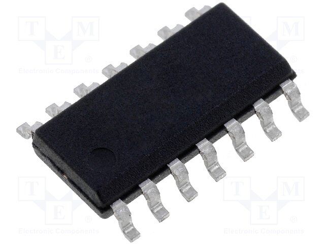
| 产品图片 |
|
| rohs | 符合RoHS无铅 / 符合限制有害物质指令(RoHS)规范要求 |
| 产品系列 | 放大器 IC,运算放大器 - 运放,STMicroelectronics LM324ADT- |
| 数据手册 | |
| 产品型号 | LM324ADT |
| 产品目录页面 | |
| 产品种类 | 运算放大器 - 运放 |
| 供应商器件封装 | 14-SO |
| 共模抑制比—最小值 | 70 dB |
| 关闭 | No Shutdown |
| 其它名称 | 497-1578-6 |
| 其它有关文件 | http://www.st.com/web/catalog/sense_power/FM123/SC61/SS1378/PF63710?referrer=70071840 |
| 包装 | Digi-Reel® |
| 压摆率 | 0.4 V/µs |
| 双重电源电压 | +/- 3 V, +/- 5 V, +/- 9 V, +/- 12 V |
| 商标 | STMicroelectronics |
| 增益带宽生成 | 1.3 MHz |
| 增益带宽积 | 1.3MHz |
| 安装类型 | 表面贴装 |
| 安装风格 | SMD/SMT |
| 封装 | Reel |
| 封装/外壳 | 14-SOIC(0.154",3.90mm 宽) |
| 封装/箱体 | SO-14 |
| 工作温度 | 0°C ~ 70°C |
| 工作电源电压 | 3 V to 30 V, +/- 1.5 V to +/- 15 V |
| 工厂包装数量 | 2500 |
| 技术 | Bipolar |
| 放大器类型 | 通用 |
| 最大双重电源电压 | +/- 15 V |
| 最大工作温度 | + 70 C |
| 最小双重电源电压 | +/- 1.5 V |
| 最小工作温度 | 0 C |
| 标准包装 | 1 |
| 电压-电源,单/双 (±) | 3 V ~ 30 V, ±1.5 V ~ 15 V |
| 电压-输入失调 | 2mV |
| 电流-电源 | 1.5mA |
| 电流-输入偏置 | 20nA |
| 电流-输出/通道 | 70mA |
| 电源电流 | 1.2 mA |
| 电路数 | 4 |
| 系列 | LM324A |
| 转换速度 | 0.4 V/us |
| 输入偏压电流—最大 | 150 nA |
| 输入参考电压噪声 | 40 nV |
| 输入补偿电压 | 7 mV |
| 输出电流 | 40 mA |
| 输出类型 | - |
| 通道数量 | 4 Channel |


- 商务部:美国ITC正式对集成电路等产品启动337调查
- 曝三星4nm工艺存在良率问题 高通将骁龙8 Gen1或转产台积电
- 太阳诱电将投资9.5亿元在常州建新厂生产MLCC 预计2023年完工
- 英特尔发布欧洲新工厂建设计划 深化IDM 2.0 战略
- 台积电先进制程称霸业界 有大客户加持明年业绩稳了
- 达到5530亿美元!SIA预计今年全球半导体销售额将创下新高
- 英特尔拟将自动驾驶子公司Mobileye上市 估值或超500亿美元
- 三星加码芯片和SET,合并消费电子和移动部门,撤换高东真等 CEO
- 三星电子宣布重大人事变动 还合并消费电子和移动部门
- 海关总署:前11个月进口集成电路产品价值2.52万亿元 增长14.8%


PDF Datasheet 数据手册内容提取
LM124, LM224x, LM324x Datasheet Low-power quad operational amplifiers Features • Wide gain bandwidth: 1.3 MHz • Input common mode voltage range includes ground QFN16 3x3 • Large voltage gain: 100 dB • Very low supply current/amplifier: 375 µA • Low input bias current: 20 nA • Low input voltage: 3 mV max. TSSOP14 • Low input offset current: 2 nA • Wide power supply range: – Single supply: 3 V to 30 V – Dual supplies: ±1.5 V to ±15 V SO14 Related products • See TSB572 and TSB611, 36 V newer technology devices, which have enhanced accuracy and ESD rating, reduced power consumption, and automotive grade qualification • See LM2902 and LM2902W for automotive grade applications Description The LM124, LM224x and LM324x consist of four independent, high gain operational amplifiers with frequency compensation implemented internally. They operate from a Product status link single power supply over a wide range of voltages. LM124, LM224x, LM324x Operation from split power supplies is also possible and the low-power supply current drain is independent of the magnitude of the power supply voltage. Product reference Part numbers LM124(1) LM124 LM224, LM224A(2), LM224x LM224W(3) LM324, LM324A, LM324x LM324W(3) 1. Prefixes: LM1, LM2, and LM3 refer to temperature range 2. Suffix A refers to enhanced Vio performance 3. Suffix W refers to enhanced ESD ratings. DS0985 - Rev 8 - September 2019 www.st.com For further information contact your local STMicroelectronics sales office.
LM124, LM224x, LM324x Pin connections and schematic diagram 1 Pin connections and schematic diagram Figure 1. Pin connections (top view) QFN16 3x3 Output 1 1 14 Output 4 Inverting input 1 2 - - 13 Inverting input 4 Non-inverting input 1 3 + + 12 Non-inverting input 4 V + 4 11 V - CC CC Non-inverting input 2 5 + + 10 Non-inverting input 3 Inverting input 2 6 - - 9 Inverting input 3 Output 2 7 8 Output 3 TSSOP14/SO14 1. The exposed pads of the QFN16 3x3 can be connected to VCC- or left floating DS0985 - Rev 8 page 2/22
LM124, LM224x, LM324x Pin connections and schematic diagram Figure 2. Schematic diagram (LM224A, LM324A, LM224W, LM324W, one channel) Figure 3. Schematic diagram (LM124, LM224, LM324, one channel) DS0985 - Rev 8 page 3/22
LM124, LM224x, LM324x Absolute maximum ratings and operating conditions 2 Absolute maximum ratings and operating conditions Table 1. Absolute maximum ratings Symbol Parameter Value Unit VCC Supply voltage ±16 or 32 Input voltage -0.3 to VCC + 0.3 LM224A, LM324A, LM224W, LM324W Vi V Input voltage -0.3 to 32 LM124, LM224, LM324 Vid Differential input voltage (1) 32 Ptot Power dissipation: D suffix 400 mW Output short-circuit duration (2) Infinite Iin Input current (3) 50 mA Tstg Storage temperature range -65 to 150 °C Tj Maximum junction temperature 150 QFN16 3x3 45 Rthja Thermal resistance junction to ambient (4) TSSOP14 100 SO14 103 °C/W QFN16 3x3 14 Rthjc Thermal resistance junction to case TSSOP14 32 SO14 31 LM224A, LM324A 800 HBM: human body model (5) LM224W, LM324W 700 ESD LM124, LM224, LM324 250 V MM: machine model (6) 100 CDM: charged device model 1500 1. Neither of the input voltages must exceed the magnitude of (VCC +) or (VCC -). 2. Short-circuits from the output to VCC can cause excessive heating if VCC > 15 V. The maximum output current is approximately 40 mA independent of the magnitude of VCC. Destructive dissipation can result from simultaneous short-circuits on all amplifiers. 3. This input current only exists when the voltage at any of the input leads is driven negative. It is due to the collector-base junction of the input PNP transistor becoming forward biased and thereby acting as an input diode clamp. In addition to this diode action, there is also an NPN parasitic action on the IC chip. This transistor action can cause the output voltages of the op amps to go to the VCC voltage level (or to ground for a large overdrive) for the time during which an input is driven negative. This is not destructive and normal output starts up again for input voltages higher than -0.3 V. 4. Short-circuits can cause excessive heating. Destructive dissipation can result from simultaneous short- circuits on all amplifiers. These are typical values given for a single layer board (except for TSSOP which is a two-layer board). 5. Human body model: 100 pF discharged through a 1.5 kΩ resistor between two pins of the device, done for all couples of pin combinations with other pins floating. 6. Machine model: a 200 pF cap is charged to the specified voltage, then discharged directly between two pins of the device with no external series resistor (internal resistor < 5 Ω), done for all couples of pin combinations with other pins floating. DS0985 - Rev 8 page 4/22
LM124, LM224x, LM324x Absolute maximum ratings and operating conditions Table 2. Operating conditions Symbol Parameter Value Unit Single supply 3 to 30 VCC Supply voltage Dual supply ±1.5 to ±15 Common-mode input voltage range 0 to VCC - 1.5 V Tamb= 25 °C VICM Common-mode input voltage range 0 to VCC -2 Tmin. ≤ Tamb ≤ Tmax. LM124 -55 to 125 TOper Operating temperature range LM224 -40 to 105 °C LM324 0 to 70 DS0985 - Rev 8 page 5/22
LM124, LM224x, LM324x Electrical characteristics 3 Electrical characteristics Table 3. V = 5 V, V = ground, V = 1.4 V, T = 25 °C (unless otherwise specified) CC+ CC- o amb Symbol Parameter Min. Typ. Max. Unit Vio Tamb = 25 °C 2 3 LM224A, LM324A, Tmin ≤ Tamb ≤ Tmax 5 LM224W, LM324W Input offset voltage (1) LM124 mV 2 5 Vio Tamb = 25 °C LM224 LM124, LM324 2 7 LM224, LM124 7 LM324 Tmin ≤ Tamb ≤ Tmax LM224 LM324 9 Tamb = 25 °C 2 20 Iio Input offset current Tmin ≤ Tamb ≤ Tmax 40 nA Tamb = 25 °C 20 100 Iib Input bias current (2) Tmin ≤ Tamb ≤ Tmax 200 Avd LRaLr =ge 2 s kigΩn, aVl ov o=l t1a.g4e V g atoin 1, 1V.4C CV += 15 V, TminT ≤am Tb a=m 2b5 ≤ ° CTmax 5205 100 V/mV Supply voltage rejection ratio, Tamb = 25 °C 65 110 SVR Rs ≤ 10 kΩ, dB VCC += 5 V to 30 V Tmin ≤ Tamb ≤ Tmax 65 Tamb = 25 °C, VCC = 5V 0.7 1.2 Tamb = 25 °C, VCC = 30 V 1.5 3 ICC Supply current, all amps, no load mA Tmin ≤ Tamb ≤ Tmax, VCC = 5 V 0.8 1.2 Tmin ≤ Tamb ≤ Tmax, VCC = 30 V 1.5 3 VCC = 30 V, Tamb = 25 °C 0 28.5 Vicm Input common mode voltage range (3) V VCC = 30 V, Tmin ≤ Tamb ≤ Tmax 0 28 Common mode rejection ratio, Tamb = 25 °C 70 80 CMR dB Rs ≤ 10 kΩ Tmin ≤ Tamb ≤ Tmax 60 Isource Output current source, Vid = 1 V VCC = 15 V, Vo = 2 V 20 40 70 mA VCC = 15 V, Vo = 2 V 10 20 Isink Output sink current, Vid = -1 V VCC = 15 V, Vo = 0.2 V 12 50 µA DS0985 - Rev 8 page 6/22
LM124, LM224x, LM324x Electrical characteristics Symbol Parameter Min. Typ. Max. Unit High level output voltage, VCC = 30 V, Tamb = 25 °C 26 27 RL = 2 kΩ Tmin ≤ Tamb ≤ Tmax 26 VOH RHLig =h 1le0v eklΩ output voltage, VCC = 30 V, TminT ≤am Tb a=m 2b5 ≤ ° CTmax 2277 28 V High level output voltage, VCC = 5 V, Tamb = 25 °C 3.5 RL = 2 kΩ Tmin ≤ Tamb ≤ Tmax 3 Tamb = 25 °C 5 20 VOL Low level output voltage, RL = 10 kΩ mV Tmin ≤ Tamb ≤ Tmax 20 VCC = 15 V, Vi = 0.5 to 3 V, SR Slew rate 0.4 V/µs RL = 2 kΩ, CL = 100 pF, unity gain VCC = 30 V, f = 100 kHz, GBP Gain bandwidth product 1.3 MHz Vin=10 mV, RL = 2 kΩ, CL=100 pF f = 1kHz, Av = 20 dB, RL = 2 kΩ, THD Total harmonic distortion 0.015 % Vo = 2 Vpp, CL = 100 pF, VCC=30 V en Equivalent input noise voltage f = 1 kHz, Rs = 100 Ω, VCC = 30 V 40 nV/√Hz DVio Input offset voltage drift 7 30 µV/°C DIio Input offset current drift 10 200 pA/°C Vo1/Vo2 Channel separation (4) 1 kHz ≤ f ≤ 20 kHZ 120 kHz 1. Vo = 1.4 V, Rs = 0 Ω, 5 V < VCC + < 30 V, 0 < Vic < VCC + - 1.5 V 2. The direction of the input current is out of the IC. This current is essentially constant, independent of the state of the output so there is no load change on the input lines. 3. The input common-mode voltage of either input signal voltage should not be allowed to go negative by more than 0.3 V. The upper end of the common-mode voltage range is (VCC +) - 1.5 V, but either or both inputs can go to 32 V without damage. 4. Due to the proximity of external components, ensure that there is no coupling originating from stray capacitance between these external parts. Typically, this can be detected at higher frequencies because this type of capacitance increases. DS0985 - Rev 8 page 7/22
LM124, LM224x, LM324x Electrical characteristic curves 4 Electrical characteristic curves Figure 4. Input bias current vs. temperature Figure 5. Output current limitation 24 21 18 A) m 15 NT ( nA) 12 RRE ( U B 9 C I T U 6 P T U 3 O 0 -55 -35 -15 5 25 45 65 85 105125 TEMPERATURE (°C) Figure 6. Input voltage range Figure 7. Supply current vs. supply voltage Figure 8. Gain bandwidth product vs. temperature Figure 9. Common-mode rejection ratio DS0985 - Rev 8 page 8/22
LM124, LM224x, LM324x Electrical characteristic curves Figure 10. Open loop frequency response Figure 11. Large signal frequency response Figure 12. Voltage follower pulse response Figure 13. Output characteristics (current sinking) Figure 14. Voltage follower pulse response (small signal) Figure 15. Output characteristics (current sourcing) DS0985 - Rev 8 page 9/22
LM124, LM224x, LM324x Electrical characteristic curves Figure 16. Input current vs. supply voltage Figure 17. Large signal voltage gain vs. temperature Figure 18. Power supply and common mode rejection Figure 19. Voltage gain vs. supply voltage ratio vs. temperature 160 R =20kΩ L B) 120 d N ( GAI 80 RL=2kΩ E G A T L 40 O V 0 10 20 30 POSITIVE SUPPLY VOLTAGE (V) DS0985 - Rev 8 page 10/22
LM124, LM224x, LM324x Typical single-supply applications 5 Typical single-supply applications Figure 21. High input Z adjustable gain DC Figure 20. AC coupled inverting amplifier instrumentation amplifier Rf 100 kΩ Rf R1 A = - 100 kΩ V R1 CI 10R 1kΩ (As shownAV =-10) R3 R4 Co 1/4 100 kΩ 100 kΩ LM11/244A eo0 2VPP e1 LM124A 1/4 eO RB RL R2 Gainadjust LM124A eI ~ R2 R63.2 kΩ 10 kΩ 2 kΩ 10R0 5kΩ VCC 100 kΩ 100 kΩ R6 R7 1/4 100 kΩ 100 kΩ LM124A C1 e2 10µF If R1 = R5 and R3 = R4 = R6 = R7 eo = [ 1 + 2 R 1 ] (e2 - e1) R2 As shown eo = 101 (e2 - e1) Figure 22. AC coupled non inverting amplifier Figure 23. DC summing amplifier R1 R2 e1 100 kΩ 100 kΩ 1 MΩ AV=1+RR21 C1 (as shown AV=11) 0.1 µF CI LM11/424A Co eo0 2 VPP e2 100 kΩ 100 kΩ LM11/424A eO RB RL 6.2 kΩ 10 kΩ e3 100 kΩ R3 eI ~ 1 MΩ R4 100 kΩ 100 kΩ VCC e4 100 kΩ C2 R5 10 µF 100 kΩ eo = e1 + e2 - e3 - e4 where (e1 + e2) ≥(e3 + e4) to keep eo ≥0 V Figure 24. Non-inverting DC gain Figure 25. Low drift peak detector AV=1+ RR21 IB 10 kΩ 1/4 eO +5 V(as shown AV=101) 1/4 IB LM11/244A eo LM124A eI LM124A 1 µF *C 2IB Zo ZI 2N929 0.001 µF R2 V) 2IB IB 1 MΩ ( 10R k1Ω eO 1 RMΩ 33 MRΩ LM11/244A IB Input current compensation 0 eI (mV) *Polycarbonate or polyethylene DS0985 - Rev 8 page 11/22
LM124, LM224x, LM324x Typical single-supply applications Figure 26. Active bandpass filter Figure 27. High input Z, DC differential amplifier R1 100 kΩ C1 For R1 = R4 CMRR depends on the following resistor ration match 330 pF R2 R3 LM11/424A 47R05 kΩ R2 R4 e1 10R M4Ω 1/4 R1 100 kΩ 100 kΩ LM124A 100 kΩ C2 R3 330 pF 100 kΩ R3 R6 1/4 10 kΩ 470 kΩ LM124A 1/4 eO +V1 LM124A Vo 1/4 LM124A R7 +V2 100 kΩ VCC R8 C3 Vo = (1 + R 4 ) (V2 - V1) 100 kΩ 10µF R3 Fo = 1 kHz Q = 50 As shown Vo = 2 * (V2 - V1) Av = 100 (40 dB) Figure 28. Using symmetrical amplifiers to reduce input current (general concept) 1/4 II IB LM124A eo eI I B 2N929 0.001µF I B I B 1/4 3 MΩ LM124A IB Aux. amplifier for 1.5 MΩ input current compensation DS0985 - Rev 8 page 12/22
LM124, LM224x, LM324x Package information 6 Package information In order to meet environmental requirements, ST offers these devices in different grades of ECOPACK packages, depending on their level of environmental compliance. ECOPACK specifications, grade definitions and product status are available at: www.st.com. ECOPACK is an ST trademark. 6.1 QFN16 3x3 package information Figure 29. QFN16 3x3 package outline DS0985 - Rev 8 page 13/22
LM124, LM224x, LM324x QFN16 3x3 package information Table 4. QFN16 3x3 mechanical data Dimensions Ref. Millimeters Inches Min. Typ. Max. Min. Typ. Max. A 0.80 0.90 1.00 0.031 0.035 0.039 A1 0 0.05 0 0.002 A3 0.20 0.008 b 0.18 0.30 0.007 0.012 D 2.90 3.00 3.10 0.114 0.118 0.122 D2 1.50 1.80 0.059 0.071 E 2.90 3.00 3.10 0.114 0.118 0.122 E2 1.50 1.80 0.059 0.071 e 0.50 0.020 L 0.30 0.50 0.012 0.020 Figure 30. QFN16 3x3 recommended footprint DS0985 - Rev 8 page 14/22
LM124, LM224x, LM324x TSSOP14 package information 6.2 TSSOP14 package information Figure 31. TSSOP14 package outline aaa Table 5. TSSOP14 package mechanical data Dimensions Ref. Millimeters Inches Min. Typ. Max. Min. Typ. Max. A 1.20 0.047 A1 0.05 0.15 0.002 0.004 0.006 A2 0.80 1.00 1.05 0.031 0.039 0.041 b 0.19 0.30 0.007 0.012 c 0.09 0.20 0.004 0.0089 D 4.90 5.00 5.10 0.193 0.197 0.201 E 6.20 6.40 6.60 0.244 0.252 0.260 E1 4.30 4.40 4.50 0.169 0.173 0.176 e 0.65 0.0256 L 0.45 0.60 0.75 0.018 0.024 0.030 L1 1.00 0.039 k 0° 8° 0° 8° aaa 0.10 0.004 DS0985 - Rev 8 page 15/22
LM124, LM224x, LM324x SO14 package information 6.3 SO14 package information Figure 32. SO14 package outline Table 6. SO14 package mechanical data Dimensions Ref. Millimeters Inches Min. Typ. Max. Min. Typ. Max. 1.75 0.069 A 1.35 1.75 0.05 0.068 A1 0.10 0.25 0.004 0.009 A2 1.10 1.65 0.04 0.06 B 0.33 0.51 0.01 0.02 C 0.19 0.25 0.007 0.009 D 8.55 8.75 0.33 0.34 E 3.80 4.0 0.15 0.15 e 1.27 0.05 H 5.80 6.20 0.22 0.24 h 0.25 0.50 0.009 0.02 L 0.40 1.27 0.015 0.05 k 8° (max.) ddd 0.10 0.004 DS0985 - Rev 8 page 16/22
LM124, LM224x, LM324x Ordering information 7 Ordering information Table 7. Order codes Order code Temperature range ESD (HBM, CDM) Vio max. @ 25 °C Package Marking LM124DT -55 °C to 125 °C 250 V, 1.5 kV 5 mV 124 SO14 LM224ADT 800 V, 1.5 kV 3 mV 224A LM224APT TSSOP14 LM224DT SO14 -40 °C to 105 °C 224 LM224PT 250 V, 1.5 kV 5 mV TSSOP14 LM224QT QFN16 3x3 K425 LM224WDT 700 V, 1.5 kV 224W SO14 LM324ADT 800 V, 1.5 kV 324A LM324APT TSSOP14 LM324AWDT 3 mV SO14 324AW LM324AWPT TSSOP14 700 V, 1.5 kV LM324WDT 0 °C to 70 °C SO14 324W LM324WPT TSSOP14 LM324DT SO14 324 LM324PT 250 V, 1.5 kV 5 mV TSSOP14 LM324QT QFN16 3x3 K427 DS0985 - Rev 8 page 17/22
LM124, LM224x, LM324x Revision history Table 8. Document revision history Date Revision Changes 1-Mar-2001 1 First release Added explanation of Vid and Vi limits in Table 2 on page 4. 1-Feb-2005 2 Updated macromodel. 1-Jun-2005 3 ESD protection inserted in Table 2 on page 4. 25-Sep-2006 4 Editorial update. Removed DIP package and all information pertaining to it Table 1: Device summary: Removed order codes LM224AN, LM224AD, LM324AN, and LM324AD; updated packaging. Table 2: Absolute maximum ratings: removed N suffix power dissipation data; updated footnotes 5 and 6. 22-Aug-2013 5 Renamed Figure 3, Figure 4, Figure 6, Figure 7, Figure 16, Figure 17, Figure 18, and Figure 19. Updated axes titles of Figure 4, Figure 5, Figure 7, and Figure 17. Removed duplicate figures. Removed Section 5: Macromodels 06-Dec-2013 6 Table 2: Absolute maximum ratings: updated ESD data for HBM and MM. LM124, LM224, LM324 and LM224W, LM324W datasheets merged with LM224A, LM324A datasheet. The following sections were reworked: Features, Description, Section 1: "Pin connections and schematic diagram", Section 2: "Absolute maximum ratings and operating conditions", and 10-Jun-2016 7 Section 3: "Electrical characteristics". The following sections were added: Related products and Section 7: "Ordering information". Packaged silhouettes, pin connections, and mechanical data were standardized and updated. Updated cover page, Section 2 Absolute maximum ratings and operating conditions and 09-Sep-2019 8 Table 3. VCC + = 5 V, VCC - = ground, Vo = 1.4 V, Tamb = 25 °C (unless otherwise specified). Updated Figure 2. Schematic diagram (LM224A, LM324A, LM224W, LM324W, one channel) and Figure 3. Schematic diagram (LM124, LM224, LM324, one channel). DS0985 - Rev 8 page 18/22
LM124, LM224x, LM324x Contents Contents 1 Pin connections and schematic diagram ...........................................2 2 Absolute maximum ratings and operating conditions ..............................4 3 Electrical characteristics...........................................................6 4 Electrical characteristic curves ....................................................8 5 Typical single-supply applications ................................................11 6 Package information..............................................................13 6.1 QFN16 3x3 package information.................................................13 6.2 TSSOP14 package information..................................................14 6.3 SO14 package information......................................................15 7 Ordering information .............................................................17 Revision history .......................................................................18 DS0985 - Rev 8 page 19/22
LM124, LM224x, LM324x List of tables List of tables Table 1. Absolute maximum ratings . . . . . . . . . . . . . . . . . . . . . . . . . . . . . . . . . . . . . . . . . . . . . . . . . . . . . . . . . . . . . 4 Table 2. Operating conditions . . . . . . . . . . . . . . . . . . . . . . . . . . . . . . . . . . . . . . . . . . . . . . . . . . . . . . . . . . . . . . . . . 5 Table 3. V = 5 V, V = ground, V = 1.4 V, T = 25 °C (unless otherwise specified) . . . . . . . . . . . . . . . . . . . . . . 6 CC+ CC- o amb Table 4. QFN16 3x3 mechanical data. . . . . . . . . . . . . . . . . . . . . . . . . . . . . . . . . . . . . . . . . . . . . . . . . . . . . . . . . . . 14 Table 5. TSSOP14 package mechanical data . . . . . . . . . . . . . . . . . . . . . . . . . . . . . . . . . . . . . . . . . . . . . . . . . . . . . 15 Table 6. SO14 package mechanical data . . . . . . . . . . . . . . . . . . . . . . . . . . . . . . . . . . . . . . . . . . . . . . . . . . . . . . . . 16 Table 7. Order codes . . . . . . . . . . . . . . . . . . . . . . . . . . . . . . . . . . . . . . . . . . . . . . . . . . . . . . . . . . . . . . . . . . . . . . 17 Table 8. Document revision history. . . . . . . . . . . . . . . . . . . . . . . . . . . . . . . . . . . . . . . . . . . . . . . . . . . . . . . . . . . . . 18 DS0985 - Rev 8 page 20/22
LM124, LM224x, LM324x List of figures List of figures Figure 1. Pin connections (top view). . . . . . . . . . . . . . . . . . . . . . . . . . . . . . . . . . . . . . . . . . . . . . . . . . . . . . . . . . . . 2 Figure 2. Schematic diagram (LM224A, LM324A, LM224W, LM324W, one channel). . . . . . . . . . . . . . . . . . . . . . . . . . . 3 Figure 3. Schematic diagram (LM124, LM224, LM324, one channel). . . . . . . . . . . . . . . . . . . . . . . . . . . . . . . . . . . . . . 3 Figure 4. Input bias current vs. temperature. . . . . . . . . . . . . . . . . . . . . . . . . . . . . . . . . . . . . . . . . . . . . . . . . . . . . . . 8 Figure 5. Output current limitation. . . . . . . . . . . . . . . . . . . . . . . . . . . . . . . . . . . . . . . . . . . . . . . . . . . . . . . . . . . . . . 8 Figure 6. Input voltage range. . . . . . . . . . . . . . . . . . . . . . . . . . . . . . . . . . . . . . . . . . . . . . . . . . . . . . . . . . . . . . . . . 8 Figure 7. Supply current vs. supply voltage . . . . . . . . . . . . . . . . . . . . . . . . . . . . . . . . . . . . . . . . . . . . . . . . . . . . . . . 8 Figure 8. Gain bandwidth product vs. temperature . . . . . . . . . . . . . . . . . . . . . . . . . . . . . . . . . . . . . . . . . . . . . . . . . . 8 Figure 9. Common-mode rejection ratio. . . . . . . . . . . . . . . . . . . . . . . . . . . . . . . . . . . . . . . . . . . . . . . . . . . . . . . . . . 8 Figure 10. Open loop frequency response. . . . . . . . . . . . . . . . . . . . . . . . . . . . . . . . . . . . . . . . . . . . . . . . . . . . . . . . . 9 Figure 11. Large signal frequency response . . . . . . . . . . . . . . . . . . . . . . . . . . . . . . . . . . . . . . . . . . . . . . . . . . . . . . . 9 Figure 12. Voltage follower pulse response . . . . . . . . . . . . . . . . . . . . . . . . . . . . . . . . . . . . . . . . . . . . . . . . . . . . . . . . 9 Figure 13. Output characteristics (current sinking) . . . . . . . . . . . . . . . . . . . . . . . . . . . . . . . . . . . . . . . . . . . . . . . . . . . 9 Figure 14. Voltage follower pulse response (small signal) . . . . . . . . . . . . . . . . . . . . . . . . . . . . . . . . . . . . . . . . . . . . . . 9 Figure 15. Output characteristics (current sourcing) . . . . . . . . . . . . . . . . . . . . . . . . . . . . . . . . . . . . . . . . . . . . . . . . . . 9 Figure 16. Input current vs. supply voltage. . . . . . . . . . . . . . . . . . . . . . . . . . . . . . . . . . . . . . . . . . . . . . . . . . . . . . . . 10 Figure 17. Large signal voltage gain vs. temperature . . . . . . . . . . . . . . . . . . . . . . . . . . . . . . . . . . . . . . . . . . . . . . . . 10 Figure 18. Power supply and common mode rejection ratio vs. temperature . . . . . . . . . . . . . . . . . . . . . . . . . . . . . . . . 10 Figure 19. Voltage gain vs. supply voltage. . . . . . . . . . . . . . . . . . . . . . . . . . . . . . . . . . . . . . . . . . . . . . . . . . . . . . . . 10 Figure 20. AC coupled inverting amplifier . . . . . . . . . . . . . . . . . . . . . . . . . . . . . . . . . . . . . . . . . . . . . . . . . . . . . . . . 11 Figure 21. High input Z adjustable gain DC instrumentation amplifier . . . . . . . . . . . . . . . . . . . . . . . . . . . . . . . . . . . . . 11 Figure 22. AC coupled non inverting amplifier . . . . . . . . . . . . . . . . . . . . . . . . . . . . . . . . . . . . . . . . . . . . . . . . . . . . . 11 Figure 23. DC summing amplifier. . . . . . . . . . . . . . . . . . . . . . . . . . . . . . . . . . . . . . . . . . . . . . . . . . . . . . . . . . . . . . 11 Figure 24. Non-inverting DC gain. . . . . . . . . . . . . . . . . . . . . . . . . . . . . . . . . . . . . . . . . . . . . . . . . . . . . . . . . . . . . . 11 Figure 25. Low drift peak detector . . . . . . . . . . . . . . . . . . . . . . . . . . . . . . . . . . . . . . . . . . . . . . . . . . . . . . . . . . . . . 11 Figure 26. Active bandpass filter . . . . . . . . . . . . . . . . . . . . . . . . . . . . . . . . . . . . . . . . . . . . . . . . . . . . . . . . . . . . . . 12 Figure 27. High input Z, DC differential amplifier. . . . . . . . . . . . . . . . . . . . . . . . . . . . . . . . . . . . . . . . . . . . . . . . . . . . 12 Figure 28. Using symmetrical amplifiers to reduce input current (general concept) . . . . . . . . . . . . . . . . . . . . . . . . . . . . 12 Figure 29. QFN16 3x3 package outline. . . . . . . . . . . . . . . . . . . . . . . . . . . . . . . . . . . . . . . . . . . . . . . . . . . . . . . . . . 13 Figure 30. QFN16 3x3 recommended footprint. . . . . . . . . . . . . . . . . . . . . . . . . . . . . . . . . . . . . . . . . . . . . . . . . . . . . 14 Figure 31. TSSOP14 package outline. . . . . . . . . . . . . . . . . . . . . . . . . . . . . . . . . . . . . . . . . . . . . . . . . . . . . . . . . . . 15 Figure 32. SO14 package outline. . . . . . . . . . . . . . . . . . . . . . . . . . . . . . . . . . . . . . . . . . . . . . . . . . . . . . . . . . . . . . 16 DS0985 - Rev 8 page 21/22
LM124, LM224x, LM324x IMPORTANT NOTICE – PLEASE READ CAREFULLY STMicroelectronics NV and its subsidiaries (“ST”) reserve the right to make changes, corrections, enhancements, modifications, and improvements to ST products and/or to this document at any time without notice. Purchasers should obtain the latest relevant information on ST products before placing orders. ST products are sold pursuant to ST’s terms and conditions of sale in place at the time of order acknowledgement. Purchasers are solely responsible for the choice, selection, and use of ST products and ST assumes no liability for application assistance or the design of Purchasers’ products. No license, express or implied, to any intellectual property right is granted by ST herein. Resale of ST products with provisions different from the information set forth herein shall void any warranty granted by ST for such product. ST and the ST logo are trademarks of ST. For additional information about ST trademarks, please refer to www.st.com/trademarks. All other product or service names are the property of their respective owners. Information in this document supersedes and replaces information previously supplied in any prior versions of this document. © 2019 STMicroelectronics – All rights reserved DS0985 - Rev 8 page 22/22