ICGOO在线商城 > 集成电路(IC) > 逻辑 - 缓冲器,驱动器,接收器,收发器 > NL37WZ07USG
 Datasheet下载
- 型号: NL37WZ07USG
- 制造商: ON Semiconductor
- 库位|库存: xxxx|xxxx
- 要求:
| 数量阶梯 | 香港交货 | 国内含税 |
| +xxxx | $xxxx | ¥xxxx |
查看当月历史价格
查看今年历史价格
NL37WZ07USG产品简介:
ICGOO电子元器件商城为您提供NL37WZ07USG由ON Semiconductor设计生产,在icgoo商城现货销售,并且可以通过原厂、代理商等渠道进行代购。 NL37WZ07USG价格参考。ON SemiconductorNL37WZ07USG封装/规格:逻辑 - 缓冲器,驱动器,接收器,收发器, Buffer, Non-Inverting 3 Element 1 Bit per Element Open Drain Output US8。您可以下载NL37WZ07USG参考资料、Datasheet数据手册功能说明书,资料中有NL37WZ07USG 详细功能的应用电路图电压和使用方法及教程。
ON Semiconductor的NL37WZ07USG是一款逻辑缓冲器,广泛应用于需要信号调理、电平转换和驱动能力增强的电路中。以下是该型号的主要应用场景:

1. 信号调理与传输:NL37WZ07USG可以用于提高信号的质量和完整性,尤其是在长距离传输或噪声环境中。它能够将微弱的输入信号放大并保持其完整性,确保信号在传输过程中不失真。

2. 电平转换:该器件可以在不同电压电平之间进行转换,例如将低电压信号(如TTL电平)转换为高电压信号(如CMOS电平),或者反之。这种特性使其适用于接口电路设计,特别是在不同标准的系统之间进行通信时。

3. 驱动能力增强:当负载较重或需要驱动多个设备时,普通的逻辑门可能无法提供足够的电流驱动能力。NL37WZ07USG具有较强的驱动能力,可以有效地驱动LED、继电器、小型电机等负载,确保这些设备正常工作。

4. 总线接口应用:在多点通信系统中,如I2C、SPI等总线接口,NL37WZ07USG可以用作缓冲器,以减少信号反射和干扰,提高通信的可靠性和稳定性。

5. 工业控制与自动化:在工业环境中,信号的可靠传输至关重要。NL37WZ07USG可以用于PLC(可编程逻辑控制器)、传感器接口等场合,确保信号在恶劣环境下的稳定传输。

6. 消费电子与家电:在消费电子产品中,如电视、音响、智能家居设备等,NL37WZ07USG可以用于内部信号处理和外部接口,提升产品的性能和用户体验。

7. 汽车电子:在汽车电子系统中,如车载娱乐系统、车身控制系统等,NL37WZ07USG可以用于信号调理和驱动,确保各个子系统的正常通信和操作。

总之,NL37WZ07USG凭借其出色的信号调理、电平转换和驱动能力,在各种电子系统中扮演着重要的角色,广泛应用于工业、消费电子、汽车等多个领域。
| 参数 | 数值 |
| 产品目录 | 集成电路 (IC)半导体 |
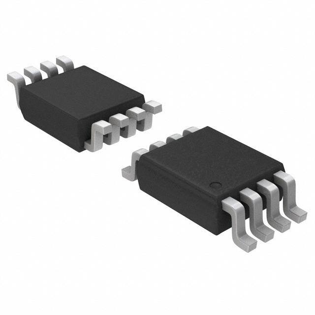
| 描述 | IC BUFF/DVR TRPL N-INV OD US8缓冲器和线路驱动器 1.65-5.5V Triple w/Open Drain |
| 产品分类 | |
| 品牌 | ON Semiconductor |
| 产品手册 | |
| 产品图片 |
|
| rohs | 符合RoHS无铅 / 符合限制有害物质指令(RoHS)规范要求 |
| 产品系列 | 逻辑集成电路,缓冲器和线路驱动器,ON Semiconductor NL37WZ07USG37WZ |
| 数据手册 | |
| 产品型号 | NL37WZ07USG |
| 产品种类 | 缓冲器和线路驱动器 |
| 传播延迟时间 | 3.7 ns |
| 低电平输出电流 | 32 mA |
| 供应商器件封装 | US8 |
| 元件数 | 3 |
| 其它名称 | NL37WZ07USGOSCT |
| 包装 | 剪切带 (CT) |
| 商标 | ON Semiconductor |
| 安装类型 | 表面贴装 |
| 安装风格 | SMD/SMT |
| 封装 | Reel |
| 封装/外壳 | 8-VFSOP(0.091",2.30mm 宽) |
| 封装/箱体 | US8-8 |
| 工作温度 | -55°C ~ 125°C |
| 工厂包装数量 | 3000 |
| 最大功率耗散 | 250 mW |
| 最大工作温度 | + 125 C |
| 最小工作温度 | - 55 C |
| 极性 | Non-Inverting |
| 标准包装 | 1 |
| 每元件位数 | 1 |
| 每芯片的通道数量 | 3 |
| 电压-电源 | 1.65 V ~ 5.5 V |
| 电流-输出高,低 | -,32mA |
| 电源电压-最大 | 5.5 V |
| 电源电压-最小 | 1.65 V |
| 电源电流 | 1 uA |
| 系列 | NL37WZ07 |
| 输入线路数量 | 3 |
| 输出类型 | Open Drain |
| 输出线路数量 | 3 |
| 逻辑类型 | CMOS |
| 逻辑系列 | LCX |
| 高电平输出电流 | - 32 mA |


PDF Datasheet 数据手册内容提取
NL37WZ07 Triple Buffer with Open Drain Outputs The NL37WZ07 is a high performance triple buffer with open drain outputs operating from a 1.65 V to 5.5 V supply. The internal circuit is composed of multiple stages, including an http://onsemi.com open drain output which provides the capability to set output switching level. This allows the NL37WZ07 to be used to interface 5 V circuits to circuits of any voltage between V and 7 V using an MARKING CC DIAGRAM external resistor and power supply. Features 8 • Extremely High Speed: tPD 2.5 ns (typical) at VCC = 5 V L7 M(cid:2) • Designed for 1.65 V to 5.5 V V Operation US8 (cid:2) CC US SUFFIX • Overvoltage Tolerant Inputs CASE 493 • 1 LVTTL Compatible − Interface Capability with 5 V TTL Logic with V = 3 V CC • L7 = Device Code LVCMOS Compatible M = Date Code* • 24 mA Output Sink Capability @ 3.0 V (cid:2) = Pb−Free Package • Near Zero Static Supply Current Substantially Reduces System (Note: Microdot may be in either location) Power Requirements *Date Code orientation may vary depending upon • manufacturing location. Chip Complexity: FET = 72 • These Devices are Pb−Free and are RoHS Compliant PIN ASSIGNMENT • NLV Prefix for Automotive and Other Applications Requiring Pin Function Unique Site and Control Change Requirements; AEC−Q100 1 IN A1 Qualified and PPAP Capable 2 OUT Y3 3 IN A2 4 GND IN A1 1 8 VCC 5 OUT Y2 6 IN A3 7 OUT Y1 OUT Y3 2 7 OUT Y1 8 VCC IN A2 3 6 IN A3 FUNCTION TABLE A Input Y Output L L GND 4 5 OUT Y2 H Z Figure 1. Pinout ORDERING INFORMATION See detailed ordering and shipping information in the package IN A1 1 OUT Y1 dimensions section on page 4 of this data sheet. IN A2 1 OUT Y2 IN A3 1 OUT Y3 Figure 2. Logic Symbol © Semiconductor Components Industries, LLC, 2012 1 Publication Order Number: April, 2012 − Rev. 8 NL37WZ07/D
NL37WZ07 MAXIMUM RATINGS Symbol Parameter Value Units VCC DC Supply Voltage −0.5 to +7.0 V VI DC Input Voltage −0.5 to +7.0 V VO DC Output Voltage −0.5 to +7.0 V IIK DC Input Diode Current mA VI < GND −50 IOK DC Output Diode Current mA VO < GND −50 IO DC Output Sink Current ±50 mA ICC DC Supply Current per Supply Pin ±100 mA IGND DC Ground Current per Ground Pin ±100 mA TSTG Storage Temperature Range −65 to +150 °C TL Lead Temperature, 1 mm from Case for 10 Seconds 260 °C TJ Junction Temperature under Bias +150 °C (cid:2)JA Thermal Resistance (Note 1) 250 °C/W PD Power Dissipation in Still Air at 85°C 250 mW MSL Moisture Sensitivity Level 1 FR Flammability Rating Oxygen Index: 28 to 34 UL 94 V−0 @ 0.125 in VESD ESD Withstand Voltage V Human Body Model (Note 2) > 2000 Machine Model (Note 3) > 150 Charged Device Model (Note 4) N/A Stresses exceeding Maximum Ratings may damage the device. Maximum Ratings are stress ratings only. Functional operation above the Recommended Operating Conditions is not implied. Extended exposure to stresses above the Recommended Operating Conditions may affect device reliability. 1. Measured with minimum pad spacing on an FR4 board, using 10 mm−by−1 inch, 2−ounce copper trace with no air flow. 2. Tested to EIA/JESD22−A114−A. 3. Tested to EIA/JESD22−A115−A. 4. Tested to JESD22−C101−A. RECOMMENDED OPERATING CONDITIONS Symbol Parameter Min Max Units VCC Supply Voltage V Operating 1.65 5.5 Data Retention Only 1.5 5.5 VI Input Voltage (Note 5) 0 5.5 V VO Output Voltage (HIGH or LOW State) 0 5.5 V TA Operating Free−Air Temperature −55 +125 °C (cid:3)t/(cid:3)V Input Transition Rise or Fall Rate ns/V VCC = 2.5 V ±0.2 V 0 20 VCC = 3.0 V ±0.3 V 0 10 VCC = 5.0 V ±0.5 V 0 5 5. Unused inputs may not be left open. All inputs must be tied to a high− or low−logic input voltage level. http://onsemi.com 2
NL37WZ07 DC ELECTRICAL CHARACTERISTICS VCC TA = 25°C −55°C (cid:2)TA (cid:2) 125°C Symbol Parameter Condition (V) Min Typ Max Min Max Units VIH High−Level Input Voltage 1.65 to 1.95 0.75 VCC 0.75 VCC V 2.3 to 5.5 0.7 VCC 0.7 VCC VIL Low−Level Input Voltage 1.65 to 1.95 0.25 VCC 0.25 VCC V 2.3 to 5.5 0.3 VCC 0.3 VCC ILKG Z−State Output Leakage VIN = VIL 1.65 to 5.5 ±5.0 ±10.0 (cid:4)A Current VOUT = VCC or GND VOL Low−Level Output IOL = 100 (cid:4)A 1.65 to 5.5 0.0 0.1 0.1 V Voltage VIN = VIH or VIL IOL = 4 mA 1.65 0.08 0.24 0.24 IOL = 8 mA 2.3 0.20 0.3 0.3 IOL = 12 mA 2.7 0.22 0.4 0.4 IOL = 16 mA 3.0 0.28 0.4 0.4 IOL = 24 mA 3.0 0.38 0.55 0.55 IOL = 32 mA 4.5 0.42 0.55 0.55 IIN Input Leakage Current VIN = 5.5 V or GND 0 to 5.5 ±0.1 ±1.0 (cid:4)A IOFF Power Off VIN = 5.5 V or 0 1 10 (cid:4)A Leakage Current VOUT = 5.5 V ICC Quiescent Supply VIN = 5.5 V or GND 5.5 1 10 (cid:4)A Current ÎÎÎÎÎÎÎÎÎÎÎÎÎÎÎÎÎÎÎÎÎÎÎÎÎÎÎÎÎÎÎÎÎ ÎÎAÎÎC EÎÎLEÎÎÎCTRÎÎICAÎÎL CÎÎHAÎÎRACÎÎTEÎÎÎRISÎÎTICÎÎS tRÎÎ = tFÎÎ = 2.ÎÎ5 nsÎÎ; CL ÎÎÎ= 50ÎÎ pF;ÎÎ RL =ÎÎÎ 500ÎÎ (cid:5) ÎÎÎÎÎÎÎÎÎÎÎÎÎÎÎÎÎÎÎÎÎÎÎÎÎÎ ÎÎÎÎÎÎÎÎÎÎÎÎÎÎÎÎÎÎÎÎÎÎÎÎÎÎÎÎÎÎTAÎÎ = 2ÎÎÎ5°CÎÎÎÎÎÎ−ÎÎ55°ÎÎC (cid:2) TÎÎÎA (cid:2)ÎÎ 125ÎΰC ÎÎÎÎ ÎÎÎÎSymÎÎbolÎÎÎÎÎÎPÎÎaraÎÎmeteÎÎr ÎÎÎÎÎÎÎÎÎÎCÎÎondÎÎitionÎÎÎÎÎÎÎÎÎÎVCÎÎC (VÎÎÎÎ) ÎÎMinÎÎÎÎÎÎTypÎÎÎÎÎÎMaxÎÎÎÎÎÎMiÎÎn ÎÎÎÎÎÎMaxÎÎÎÎÎÎUnÎÎits ÎÎtPÎZL ÎÎPÎropaÎgatioÎn DÎelayÎÎÎÎRÎÎL = RÎÎ1 = ÎÎ500 ÎÎ(cid:5), CÎÎL = 5ÎÎ0 pFÎÎÎÎÎÎ1.8 Îα0.1ÎÎÎÎ5 ÎÎÎÎÎÎÎÎÎÎÎÎÎÎ7.8ÎÎÎÎÎÎÎÎÎÎÎÎÎÎ7.8ÎÎÎÎÎnÎs (Figure 3 and 4) ÎÎÎÎÎÎÎÎÎÎÎÎÎRÎÎL = RÎÎ1 = ÎÎ500 ÎÎ(cid:5), CÎÎL = 5ÎÎ0 pFÎÎÎÎÎÎ2.5ÎÎ ±0.ÎÎÎÎ2 ÎÎ1.2ÎÎÎÎÎÎ3.7ÎÎÎÎÎÎ5.8ÎÎÎÎÎÎ1.2ÎÎÎÎÎÎÎÎ6.4ÎÎÎÎÎÎ ÎÎÎÎÎÎÎÎÎÎÎÎÎRÎÎL = RÎÎ1 = ÎÎ500 ÎÎ(cid:5), CÎÎL = 5ÎÎ0 pFÎÎÎÎÎÎ3.3ÎÎ ±0.ÎÎÎÎ3 ÎÎ0.8ÎÎÎÎÎÎ2.9ÎÎÎÎÎÎ4.4ÎÎÎÎÎÎ0.8ÎÎÎÎÎÎÎÎ4.8ÎÎÎÎÎÎ ÎÎÎÎÎÎÎÎÎÎÎÎÎÎÎÎÎÎÎÎÎÎÎÎRÎÎL = RÎÎ1 = ÎÎ500 ÎÎ(cid:5), CÎÎL = 5ÎÎ0 pFÎÎÎÎÎÎ5.0ÎÎ ±0.ÎÎÎÎ5 ÎÎ0.5ÎÎÎÎÎÎ2.3ÎÎÎÎÎÎ3.5ÎÎÎÎÎÎ0.5ÎÎÎÎÎÎÎÎ3.9ÎÎÎÎÎÎÎÎ ÎÎtPÎLZ ÎÎPÎropaÎgatioÎn DÎelayÎÎÎÎRÎÎL = RÎÎ1 = ÎÎ500 ÎÎ(cid:5), CÎÎL = 5ÎÎ0 pFÎÎÎÎÎÎ1.8 Îα0.1ÎÎÎÎ5 ÎÎÎÎÎÎÎÎÎÎÎÎÎÎ7.8ÎÎÎÎÎÎÎÎÎÎÎÎÎÎ7.8ÎÎÎÎÎnÎs (Figure 3 and 4) ÎÎÎÎÎÎÎÎÎÎÎÎÎRÎÎL = RÎÎ1 = ÎÎ500 ÎÎ(cid:5), CÎÎL = 5ÎÎ0 pFÎÎÎÎÎÎ2.5ÎÎ ±0.ÎÎÎÎ2 ÎÎ1.2ÎÎÎÎÎÎ2.8ÎÎÎÎÎÎ5.8ÎÎÎÎÎÎ1.2ÎÎÎÎÎÎÎÎ6.4ÎÎÎÎÎÎ ÎÎÎÎÎÎÎÎÎÎÎÎÎRÎÎL = RÎÎ1 = ÎÎ500 ÎÎ(cid:5), CÎÎL = 5ÎÎ0 pFÎÎÎÎÎÎ3.3ÎÎ ±0.ÎÎÎÎ3 ÎÎ0.8ÎÎÎÎÎÎ2.1ÎÎÎÎÎÎ4.4ÎÎÎÎÎÎ0.8ÎÎÎÎÎÎÎÎ4.8ÎÎÎÎÎÎ ÎÎÎÎÎÎÎÎÎÎÎÎRÎL = RÎ1 = Î500 Î(cid:5), CÎL = 5Î0 pFÎÎÎ5.0Î ±0.ÎÎ5 Î0.5ÎÎÎ1.4ÎÎÎ3.5ÎÎÎ0.5ÎÎÎÎ3.9ÎÎÎÎ CAPACITIVE CHARACTERISTICS Symbol Parameter Condition Typical Units CIN Input Capacitance VCC = 5.5 V, VI = 0 V or VCC 2.5 pF COUT Output Capacitance VCC = 5.5 V, VI = 0 V or VCC 4.0 pF CPD Power Dissipation Capacitance (Note 6) 10 MHz, VCC = 5.5 V, VI = 0 V or VCC 4.0 pF 6. CPD is defined as the value of the internal equivalent capacitance which is calculated from the operating current consumption without load. Apovwerearg ceo onpseurmatpintigo nc;u PrrDe n=t cCaPnD b (cid:2)e VoCbCta2i n(cid:2)e fdin b(cid:2)y thICeC e (cid:2)q uVaCtCio.n: ICC(OPR) = CPD (cid:2) VCC (cid:2) fin (cid:2) ICC. CPD is used to determine the no−load dynamic http://onsemi.com 3
NL37WZ07 VCC A 50% GND tPZL tPLZ HIGH IMPEDANCE Y 50% VCC VOL +0.3 V Figure 3. Switching Waveforms VCC PULSE R1 VCC x 2 DUT GENERATOR RT CL RL RT = ZOUT of pulse generator (typically 50 (cid:5)) Figure 4. Test Circuit DEVICE ORDERING INFORMATION Device Order Number Package Shipping† NL37WZ07USG US8 3000 / Tape & Reel (Pb−Free) NLV37WZ07USG* US8 3000 / Tape & Reel (Pb−Free) †For information on tape and reel specifications, including part orientation and tape sizes, please refer to our Tape and Reel Packaging Specifications Brochure, BRD8011/D. *NLV Prefix for Automotive and Other Applications Requiring Unique Site and Control Change Requirements; AEC−Q100 Qualified and PPAP Capable. http://onsemi.com 4
NL37WZ07 PACKAGE DIMENSIONS US8 CASE 493−02 ISSUE B NOTES: 1. DIMENSIONING AND TOLERANCING PER −X− ANSI Y14.5M, 1982. A 2. CONTROLLING DIMENSION: MILLIMETERS. J 3. DIMENSION “A” DOES NOT INCLUDE MOLD 8 5 −Y− FLASH, PROTRUSION OR GATE BURR. MOLD FLASH. PROTRUSION AND GATE BURR SHALL NOT EXCEED 0.140 MM (0.0055”) PER SIDE. DETAIL E 4. DIMENSION “B” DOES NOT INCLUDE INTER−LEAD FLASH OR PROTRUSION. B L INTER−LEAD FLASH AND PROTRUSION SHALL NOT E3XCEED 0.140 (0.0055”) PER SIDE. 5. LEAD FINISH IS SOLDER PLATING WITH THICKNESS OF 0.0076−0.0203 MM. (300−800 “). 6. ALL TOLERANCE UNLESS OTHERWISE 1 4 R SPECIFIED ±0.0508 (0.0002 “). G S P U MILLIMETERS INCHES DIM MIN MAX MIN MAX A 1.90 2.10 0.075 0.083 B 2.20 2.40 0.087 0.094 C C 0.60 0.90 0.024 0.035 −T− K 0.10 (0.004) T H DF 00..1270 00..2355 00..000078 00..001140 SEATING D G 0.50 BSC 0.020 BSC PLANE N H 0.40 REF 0.016 REF 0.10 (0.004) M T X Y R 0.10 TYP J 0.10 0.18 0.004 0.007 K 0.00 0.10 0.000 0.004 L 3.00 3.20 0.118 0.126 V M MN 05 (cid:3)(cid:3) 106 (cid:3)(cid:3) 50 (cid:3)(cid:3) 106 (cid:3)(cid:3) P 0.23 0.34 0.010 0.013 R 0.23 0.33 0.009 0.013 S 0.37 0.47 0.015 0.019 U 0.60 0.80 0.024 0.031 F V 0.12 BSC 0.005 BSC DETAIL E SOLDERING FOOTPRINT* 3.8 0.15 0.50 1.8 0.0197 0.07 0.30 0.012 1.0 (cid:3) (cid:4) mm 0.0394 SCALE 8:1 inches *For additional information on our Pb−Free strategy and soldering details, please download the ON Semiconductor Soldering and Mounting Techniques Reference Manual, SOLDERRM/D. ON Semiconductor and are registered trademarks of Semiconductor Components Industries, LLC (SCILLC). SCILLC reserves the right to make changes without further notice to any products herein. SCILLC makes no warranty, representation or guarantee regarding the suitability of its products for any particular purpose, nor does SCILLC assume any liability arising out of the application or use of any product or circuit, and specifically disclaims any and all liability, including without limitation special, consequential or incidental damages. “Typical” parameters which may be provided in SCILLC data sheets and/or specifications can and do vary in different applications and actual performance may vary over time. All operating parameters, including “Typicals” must be validated for each customer application by customer’s technical experts. SCILLC does not convey any license under its patent rights nor the rights of others. SCILLC products are not designed, intended, or authorized for use as components in systems intended for surgical implant into the body, or other applications intended to support or sustain life, or for any other application in which the failure of the SCILLC product could create a situation where personal injury or death may occur. Should Buyer purchase or use SCILLC products for any such unintended or unauthorized application, Buyer shall indemnify and hold SCILLC and its officers, employees, subsidiaries, affiliates, and distributors harmless against all claims, costs, damages, and expenses, and reasonable attorney fees arising out of, directly or indirectly, any claim of personal injury or death associated with such unintended or unauthorized use, even if such claim alleges that SCILLC was negligent regarding the design or manufacture of the part. SCILLC is an Equal Opportunity/Affirmative Action Employer. This literature is subject to all applicable copyright laws and is not for resale in any manner. PUBLICATION ORDERING INFORMATION LITERATURE FULFILLMENT: N. American Technical Support: 800−282−9855 Toll Free ON Semiconductor Website: www.onsemi.com Literature Distribution Center for ON Semiconductor USA/Canada P.O. Box 5163, Denver, Colorado 80217 USA Europe, Middle East and Africa Technical Support: Order Literature: http://www.onsemi.com/orderlit Phone: 303−675−2175 or 800−344−3860 Toll Free USA/Canada Phone: 421 33 790 2910 Fax: 303−675−2176 or 800−344−3867 Toll Free USA/Canada Japan Customer Focus Center For additional information, please contact your local Email: orderlit@onsemi.com Phone: 81−3−5817−1050 Sales Representative http://onsemi.com NL37WZ07/D 5
Mouser Electronics Authorized Distributor Click to View Pricing, Inventory, Delivery & Lifecycle Information: O N Semiconductor: NL37WZ07USG