ICGOO在线商城 > 集成电路(IC) > 逻辑 - 缓冲器,驱动器,接收器,收发器 > 74VCX164245MTDX

 Datasheet下载
- 型号: 74VCX164245MTDX
- 制造商: Fairchild Semiconductor
- 库位|库存: xxxx|xxxx
- 要求:
| 数量阶梯 | 香港交货 | 国内含税 |
| +xxxx | $xxxx | ¥xxxx |
查看当月历史价格
查看今年历史价格
74VCX164245MTDX产品简介:
ICGOO电子元器件商城为您提供74VCX164245MTDX由Fairchild Semiconductor设计生产,在icgoo商城现货销售,并且可以通过原厂、代理商等渠道进行代购。 74VCX164245MTDX价格参考。Fairchild Semiconductor74VCX164245MTDX封装/规格:逻辑 - 缓冲器,驱动器,接收器,收发器, Transceiver, Non-Inverting 2 Element 8 Bit per Element 3-State Output 48-TSSOP。您可以下载74VCX164245MTDX参考资料、Datasheet数据手册功能说明书,资料中有74VCX164245MTDX 详细功能的应用电路图电压和使用方法及教程。
ON Semiconductor(现为安森美半导体)的型号 74VCX164245MTDX 是一款逻辑器件,属于缓冲器、驱动器、接收器和收发器类别。该器件广泛应用于需要高速数据传输和信号转换的场景。以下是其主要应用场景:

 1. 数据总线切换与扩展
   - 该芯片支持双向数据传输,适用于多路数据总线之间的切换和扩展。
   - 在嵌入式系统中,用于连接主处理器与外设(如存储器、显示器或通信模块),实现高效的数据交换。

 2. 工业自动化
   - 在工业控制领域,用于信号隔离和增强驱动能力,确保信号在长距离传输时不失真。
   - 支持多点通信协议,例如 CAN、SPI 或 I2C 总线,在复杂工业环境中实现可靠的数据传输。

 3. 消费电子
   - 应用于电视、音响、游戏机等消费电子产品中,用于管理内部数据流和外部接口。
   - 提供低功耗特性,适合便携式设备(如平板电脑或智能音箱)。

 4. 通信设备
   - 在网络路由器、交换机或调制解调器中,用于信号放大和缓冲,以提高数据传输速度和稳定性。
   - 其低传播延迟特性使其非常适合高速通信应用。

 5. 汽车电子
   - 用于车载娱乐系统、导航系统和驾驶辅助系统中的数据传输。
   - 满足汽车级可靠性要求,能够在极端温度和振动条件下正常工作。

 6. 医疗设备
   - 在医疗监测设备(如心率仪、血压计)中,用于处理传感器数据并将其传递到显示或存储单元。
   - 提供高精度和低噪声性能,确保数据准确性。

 特性总结:
- 低功耗:适合对能效要求较高的应用。
- 高速性能:支持高达 100 MHz 的工作频率。
- 宽电压范围:兼容多种电源电压(1.65V 至 3.6V),适应不同设计需求。
- 小型封装:节省电路板空间,适合紧凑型设计。

这款芯片凭借其高性能和灵活性,成为许多现代电子系统中不可或缺的关键组件。
| 参数 | 数值 |
| 产品目录 | 集成电路 (IC)半导体 |
| 描述 | IC TRANSCEIVER 16BIT 48TSSOP总线收发器 16-Bit Dual Translating Xceiver |
| 产品分类 | |
| 品牌 | Fairchild Semiconductor |
| 产品手册 | |
| 产品图片 |
|
| rohs | 符合RoHS无铅 / 符合限制有害物质指令(RoHS)规范要求 |
| 产品系列 | 逻辑集成电路,总线收发器,Fairchild Semiconductor 74VCX164245MTDX74VCX |
| 数据手册 | |
| 产品型号 | 74VCX164245MTDX |
| 产品培训模块 | http://www.digikey.cn/PTM/IndividualPTM.page?site=cn&lang=zhs&ptm=1340 |
| 产品种类 | 总线收发器 |
| 传播延迟时间 | 6.2 ns |
| 低电平输出电流 | 24 mA |
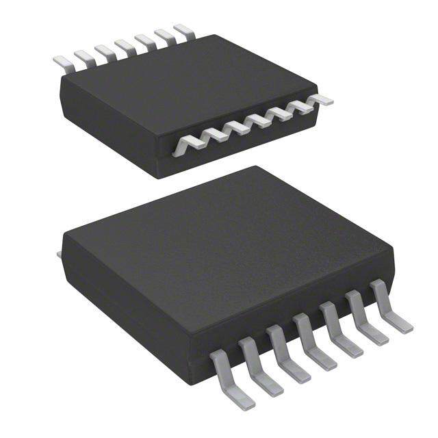
| 供应商器件封装 | 48-TSSOP |
| 元件数 | 2 |
| 其它名称 | 74VCX164245MTDXCT |
| 功能 | 16-Bit D Flip-Flop |
| 包装 | 剪切带 (CT) |
| 单位重量 | 421 mg |
| 商标 | Fairchild Semiconductor |
| 安装类型 | 表面贴装 |
| 安装风格 | SMD/SMT |
| 封装 | Reel |
| 封装/外壳 | 48-TFSOP(0.240",6.10mm 宽) |
| 封装/箱体 | TSSOP-48 |
| 工作温度 | -40°C ~ 85°C |
| 工厂包装数量 | 1000 |
| 最大工作温度 | + 85 C |
| 最小工作温度 | - 40 C |
| 极性 | Non-Inverting |
| 标准包装 | 1 |
| 每元件位数 | 8 |
| 每芯片的通道数量 | 16 |
| 电压-电源 | 1.65 V ~ 2.7 V,2.3 V ~ 3.6 V |
| 电流-输出高,低 | 18mA, 18mA; 24mA, 24mA |
| 电源电压-最大 | 2.7 V, 3.6 V |
| 电源电压-最小 | 1.65 V, 2.3 V |
| 电路数量 | 1 |
| 系列 | 74VCX164245 |
| 输入电平 | CMOS |
| 输出电平 | CMOS |
| 输出类型 | 3-State |
| 逻辑类型 | CMOS |
| 逻辑系列 | 74VC |
| 高电平输出电流 | - 24 mA |


- 商务部:美国ITC正式对集成电路等产品启动337调查
- 曝三星4nm工艺存在良率问题 高通将骁龙8 Gen1或转产台积电
- 太阳诱电将投资9.5亿元在常州建新厂生产MLCC 预计2023年完工
- 英特尔发布欧洲新工厂建设计划 深化IDM 2.0 战略
- 台积电先进制程称霸业界 有大客户加持明年业绩稳了
- 达到5530亿美元!SIA预计今年全球半导体销售额将创下新高
- 英特尔拟将自动驾驶子公司Mobileye上市 估值或超500亿美元
- 三星加码芯片和SET,合并消费电子和移动部门,撤换高东真等 CEO
- 三星电子宣布重大人事变动 还合并消费电子和移动部门
- 海关总署:前11个月进口集成电路产品价值2.52万亿元 增长14.8%


PDF Datasheet 数据手册内容提取
Is Now Part of To learn more about ON Semiconductor, please visit our website at www.onsemi.com Please note: As part of the Fairchild Semiconductor integration, some of the Fairchild orderable part numbers will need to change in order to meet ON Semiconductor’s system requirements. Since the ON Semiconductor product management systems do not have the ability to manage part nomenclature that utilizes an underscore (_), the underscore (_) in the Fairchild part numbers will be changed to a dash (-). This document may contain device numbers with an underscore (_). Please check the ON Semiconductor website to verify the updated device numbers. The most current and up-to-date ordering information can be found at www.onsemi.com. Please email any questions regarding the system integration to Fairchild_questions@onsemi.com. ON Semiconductor and the ON Semiconductor logo are trademarks of Semiconductor Components Industries, LLC dba ON Semiconductor or its subsidiaries in the United States and/or other countries. ON Semiconductor owns the rights to a number of patents, trademarks, copyrights, trade secrets, and other intellectual property. A listing of ON Semiconductor’s product/patent coverage may be accessed at www.onsemi.com/site/pdf/Patent-Marking.pdf. ON Semiconductor reserves the right to make changes without further notice to any products herein. ON Semiconductor makes no warranty, representation or guarantee regarding the suitability of its products for any particular purpose, nor does ON Semiconductor assume any liability arising out of the application or use of any product or circuit, and specifically disclaims any and all liability, including without limitation special, consequential or incidental damages. Buyer is responsible for its products and applications using ON Semiconductor products, including compliance with all laws, regulations and safety requirements or standards, regardless of any support or applications information provided by ON Semiconductor. “Typical” parameters which may be provided in ON Semiconductor data sheets and/or specifications can and do vary in different applications and actual performance may vary over time. All operating parameters, including “Typicals” must be validated for each customer application by customer’s technical experts. ON Semiconductor does not convey any license under its patent rights nor the rights of others. ON Semiconductor products are not designed, intended, or authorized for use as a critical component in life support systems or any FDA Class 3 medical devices or medical devices with a same or similar classification in a foreign jurisdiction or any devices intended for implantation in the human body. Should Buyer purchase or use ON Semiconductor products for any such unintended or unauthorized application, Buyer shall indemnify and hold ON Semiconductor and its officers, employees, subsidiaries, affiliates, and distributors harmless against all claims, costs, damages, and expenses, and reasonable attorney fees arising out of, directly or indirectly, any claim of personal injury or death associated with such unintended or unauthorized use, even if such claim alleges that ON Semiconductor was negligent regarding the design or manufacture of the part. ON Semiconductor is an Equal Opportunity/Affirmative Action Employer. This literature is subject to all applicable copyright laws and is not for resale in any manner.
7 4 March 2000 V Revised June 2005 C X 1 6 4 74VCX164245 2 4 5 Low Voltage 16-Bit Dual Supply Translating Transceiver L o with 3-STATE Outputs w V o General Description Features l t a The VCX164245 is a dual supply, 16-bit translating trans- (cid:1) Bidirectional interface between busses ranging from g ceiver that is designed for two way asynchronous commu- 1.65V to 3.6V e nication between busses at different supply voltages by (cid:1) Supports Live Insertion and Withdrawal (Note 1) 16 pV31..rC66oCV5vBVi da, inwntodgh 2iVtcr.Chu7C eVisA .s ,t( ihgwVenCh aiChclA ihgt r hmaisen utrsh slpeat o tblitooeewnn .lete iTars hlps re oat thsiela unonptpi paeollyrr ra aertaiiqln iuolgsap acle tort oan2 ts.iV3nisVCgt C aotoBtf (cid:1) Starrt21ic48 DmmriAAv e@@ (I O32H..03/VVIO LVV)CCCC -Bit Du faollro wpsro fpoer rtr adnesvlaicteio no fproemra t1io.8nV.) toT 2h.i5s Vd buuasl sessu ptop lbyu sdseessig ant (cid:1) Usre6s mprAo pr@iet a1r.y6 5nVo isVeC/CEMI reduction circuitry al S a higher potential, up to 3.3V. The Transmit/Receive (T/R) input determines the direction (cid:1) Functionally compatible with 74 series 16245 up of data flow. Transmit (active-HIGH) enables data from A (cid:1) Latchup performance exceeds 300 mA p l Ports to B Ports. Receive (active-LOW) enables data from (cid:1) ESD performance: y B Ports to A Ports. The Output Enable (OE) input, when Human Body Model !2000V T r HIGH, disables both A and B Ports by placing them in a Machine model !200V a High-Z condition. The A Port interfaces with the lower volt- n age bus (1.8V (cid:16) 2.5V). The B Port interfaces with the (cid:1) Also packaged in plastic Fine-Pitch Ball Grid Array s higher voltage bus (2.7V (cid:16) 3.3V). Also the VCX164245 is (FBGA) la t designed so that the control pins (T/Rn, OEn) are supplied in bTyh eV C7C4BV.CX164245 is suitable for mixed voltage applica- Note 1: To ensure the high impedance state during power up or power g Tr tions such as notebook computers using a 1.8V CPU and down, OEn should be tied to VCCB through a pull up resistor. The minimum a 3.3V peripheral components. It is fabricated with an value of the resistor is determined by the current sourcing capability of the n driver. s Advanced CMOS technology to achieve high speed opera- c tion while maintaining low CMOS power dissipation. e i v e r Ordering Code: w it h Order Number Package Number Package Description 3 74VCX164245G BGA54A 54-Ball Fine-Pitch Ball Grid Array (FBGA), JEDEC MO-205, 5.5mm Wide - S (Note 2)(Note 3) T 74VCX164245MTD MTD48 48-Lead Thin Shrink Small Outline Package (TSSOP), JEDEC MO-153, 6.1mm Wide A (Note 3) T E Note 2: Ordering Code “G” indicates Trays. O Note 3: Device also available in Tape and Reel. Specify by appending suffix letter “X” to the ordering code. u t Logic Diagram p u t s © 2005 Fairchild Semiconductor Corporation DS500159 www.fairchildsemi.com
5 4 Connection Diagrams Pin Descriptions 2 4 6 1 Pin Assignment for TSSOP Pin Names Description X C OEn Output Enable Input (Active LOW) V 4 T/Rn Transmit/Receive Input 7 A0–A15 Side A Inputs or 3-STATE Outputs B0–B15 Side B Inputs or 3-STATE Outputs NC No Connect FBGA Pin Assignments 1 2 3 4 5 6 A B0 NC T/R1 OE1 NC A0 B B2 B1 NC NC A1 A2 C B4 B3 VCCB VCCA A3 A4 D B6 B5 GND GND A5 A6 E B8 B7 GND GND A7 A8 F B10 B9 GND GND A9 A10 G B12 B11 VCCB VCCA A11 A12 H B14 B13 NC NC A13 A14 J B15 NC T/R2 OE2 NC A15 Truth Tables Inputs Pin Assignment for FBGA Outputs OE1 T/R1 L L Bus B0–B7 Data to Bus A0–A7 L H Bus A0–A7 Data to Bus B0–B7 H X HIGH Z State on A0–A7, B0–B7 Inputs Outputs OE2 T/R2 L L Bus B8–B15 Data to Bus A8–A15 L H Bus A8–A15 Data to Bus B8–B15 H X HIGH-Z State on A8–A15, B8–B15 (Top Through View) H HIGH Voltage Level L LOW Voltage Level X Immaterial (HIGH or LOW, inputs may not float) Z High Impedance Translator Power Up Sequence Recommendations To guard against power up problems, some simple guide- sourcing capability of the driver. Second, the T/Rn control lines need to be adhered to. The VCX164245 is designed pins should be placed at logic low (0V) level, this will so that the control pins (T/Rn, OEn) are supplied by VCCB. ensure that the B-side bus pins are configured as inputs to Therefore the first recommendation is to begin by powering help guard against bus contention and oscillations. B-side up the control side of the device, VCCB. The OEn control Data Inputs should be driven to a valid logic level (0V or pins should be ramped with or ahead of VCCB, this will VCCB), this will prevent excessive current draw and oscilla- guard against bus contentions and oscillations as all A Port tions. VCCA can then be powered up after VCCB, but should and B Port outputs will be disabled. To ensure the high never exceed the VCCB voltage level. Upon completion of impedance state during power up or power down, OEn these steps the device can then be configured for the users should be tied to VCCB through a pull up resistor. The mini- desired operation. Following these steps will help to pre- mum value of the resistor is determined by the current vent possible damage to the translator device as well as other system components. www.fairchildsemi.com 2
7 Logic Diagrams 4 V C X 1 6 4 2 4 5 Please note that these diagrams are provided only for the understanding of logic operations and should not be used to estimate propagation delays. 3 www.fairchildsemi.com
5 4 Absolute Maximum Ratings Recommended Operating 2 (Note 4) 4 Conditions 6 Supply Voltage (Note 6) 1 X VCCA (cid:16)0.5V to VCCB Power Supply (Note 7) VC VCCB (cid:16)0.5V to 4.6V VCCA 1.65V to 2.7V 4 DC Input Voltage (VI) (cid:16)0.5V to (cid:14)4.6V VCCB 2.3V to 3.6V 7 DC Output Voltage (VI/O) Input Voltage (VI) @ OE, T/R 0V to VCCB Outputs 3-STATE (cid:16)0.5V to (cid:14)4.6V Input/Output Voltage (VI/O) Outputs Active (Note 5) An 0V to VCCA An (cid:16)0.5V to VCCA (cid:14) 0.5V Bn 0V to VCCB Bn (cid:16)0.5V to VCCB (cid:14) 0.5V Output Current in IOH/IOL DC Input Diode Current (IIK) VCCA 2.3V to 2.7V r18 mA VI (cid:31) 0V (cid:16)50 mA VCCA 1.65V to 1.95V r6 mA DC Output Diode Current (IOK) VCCB 3.0V to 3.6V r24 mA VO (cid:31) 0V (cid:16)50 mA VCCB 2.3V to 2.7V r18 mA VO ! VCC (cid:14)50 mA Free Air Operating Temperature (TA) (cid:16)40qC to (cid:14)85qC DC Output Source/Sink Current r50 mA Minimum Input Edge Rate (’t/’V) (IOH/IOL) VIN 0.8V to 2.0V, VCC 3.0V 10 ns/V DC VCC or Ground Current r100 mA Note 4: The “Absolute Maximum Ratings” are those values beyond which the safety of the device cannot be guaranteed. The device should not be Supply Pin (ICC or Ground) operated at these limits. The parametric values defined in the Electrical Storage Temperature (TSTG) (cid:16)65qC to (cid:14)150qC Characteristics tables are not guaranteed at the absolute maximum ratings. The “Recommended Operating Conditions” table will define the conditions for actual device operation. Note 5: IO Absolute Maximum Rating must be observed. Note 6: Unused inputs or I/O pins must be held HIGH or LOW. They may not float. Note 7: Operation requires: VCCA d VCCB DC Electrical Characteristics (1.65V (cid:1) V (cid:2) 1.95V, 2.3V (cid:1) V (cid:2) 2.7V) CCA CCB VCCA VCCB Symbol Parameter Conditions Min Max Units (V) (V) VIHA HIGH Level Input Voltage An 1.65(cid:16)1.95 2.3(cid:16)2.7 0.65 x VCC V VIHB Bn, T/R, OE 1.65(cid:16)1.95 2.3(cid:16)2.7 1.6 V VILA LOW Level Input Voltage An 1.6(cid:16)1.95 2.3(cid:16)2.7 0.35 x VCC V VILB Bn, T/R, OE 1.65(cid:16)1.95 2.3(cid:16)2.7 0.7 V VOHA HIGH Level Output Voltage IOH (cid:16)100 PA 1.65(cid:16)1.95 2.3(cid:16)2.7 VCCA(cid:16)0.2 V IOH (cid:16)6 mA 1.65 2.3(cid:16)2.7 1.25 VOHB HIGH Level Output Voltage IOH (cid:16)100 PA 1.65(cid:16)1.95 2.3(cid:16)2.7 VCCB(cid:16)0.2 V IOH (cid:16)18 mA 1.65(cid:16)1.95 2.3 1.7 VOLA LOW Level Output Voltage IOL 100 PA 1.65(cid:16)1.95 2.3(cid:16)2.7 0.2 V IOL 6 mA 1.65 2.3(cid:16)2.7 0.3 VOLB LOW Level Output Voltage IOL 100 PA 1.65(cid:16)1.95 2.3(cid:16)2.7 0.2 V IOL 18 mA 1.65(cid:16)1.95 2.3 0.6 II Input Leakage Current @ OE, T/R 0V d VI d 3.6V 1.65(cid:16)1.95 2.3(cid:16)2.7 r5.0 PA IOZ 3-STATE Output Leakage 0V d VO d 3.6V OE VCCB 1.65(cid:16)1.95 2.3(cid:16)2.7 r10 PA VI VIH or VIL IOFF Power OFF Leakage Current 0d (VI, VO) d 3.6V 0 0 10 PA ICCA/ICCB Quiescent Supply Current, An VCCA or GND 1.65(cid:16)1.95 2.3(cid:16)2.7 20 PA per supply, VCCA / VCCB Bn, OE, & T/R VCCB or GND VCCA d An d 3.6V 1.65(cid:16)1.95 2.3(cid:16)2.7 r20 PA VCCB d Bn, OE, T/R d 3.6V ’ICC Increase in ICC per Input, Bn, T/R, OE VI VCCB – 0.6V 1.65(cid:16)1.95 2.3(cid:16)2.7 750 PA Increase in ICC per Input, An VI VCCA – 0.6V 1.65(cid:16)1.95 2.3(cid:16)2.7 750 PA www.fairchildsemi.com 4
7 DC Electrical Characteristics (1.65V (cid:1) V (cid:2) 1.95V, 3.0V (cid:1) V (cid:2) 3.6V) 4 CCA CCB V C VCCA VCCB X Symbol Parameter Conditions Min Max Units 1 (V) (V) 6 VIHA HIGH Level An 1.65–1.95 3.0–3.6 0.65 x VCC V 42 VIHB Input Voltage Bn, T/R, OE 1.65–1.95 3.0–3.6 2.0 V 45 VILA LOW Level An 1.65–1.95 3.0–3.6 0.35 x VCC V VILB Input Voltage Bn, T/R, OE 1.65–1.95 3.0–3.6 0.8 V VOHA HIGH Level Output Voltage IOH (cid:16)100 PA 1.65–1.95 3.0–3.6 VCCA–0.2 V IOH (cid:16)6 mA 1.65 3.0–3.6 1.25 VOHB HIGH Level Output Voltage IOH (cid:16)100 PA 1.65–1.95 3.0–3.6 VCCA–0.2 V IOH (cid:16)24 mA 1.65–1.95 3.0 2.2 VOLA LOW Level Output Voltage IOL 100 PA 1.65–1.95 3.0–3.6 0.2 V IOL 6 mA 1.65 3.0–3.6 0.3 VOLB LOW Level Output Voltage IOL 100 PA 1.65–1.95 3.0–3.6 0.2 V IOL 24 mA 1.65–1.95 3.0 0.55 II Input Leakage Current @ OE, T/R 0V d VI d 3.6V 1.65–1.95 3.0–3.6 r5.0 PA IOZ 3-STATE Output Leakage 0V d VO d 3.6V OE* VCCB 1.65–1.95 3.0–3.6 r10 PA VI VIH or VIL IOFF Power Off Leakage Current 0 d (VI, VO) d 3.6V 0 0 10 PA ICCA/ICCB Quiescent Supply Current, An VCCA or GND 1.65–1.95 3.0–3.6 20 PA per supply, VCCA/VCCB Bn, OE, & T/R VCCB or GND VCCA d An d 3.6V 1.65–1.95 3.0–3.6 r20 PA VCCB d Bn, OE, T/R d 3.6V ’ICC Increase in ICC per Input, Bn, T/R, OE VI VCCB (cid:16) 0.6V 1.65–1.95 3.0–3.6 750 PA Increase in ICC per Input, An VI VCCA (cid:16) 0.6V 1.65–1.95 3.0–3.6 750 PA DC Electrical Characteristics (2.3V (cid:1) V (cid:2) 2.7V, 3.0V (cid:2) V (cid:2) 3.6V) CCA CCB VCCA VCCB Symbol Parameter Conditions Min Max Units (V) (V) VIHA HIGH Level Input Voltage An 2.3–2.7 3.0–3.6 1.6 V VIHB Bn, T/R, OE 2.3–2.7 3.0–3.6 2.0 V VILA LOW Level Input Voltage An 2.3–2.7 3.0–3.6 0.7 V VILB Bn, T/R, OE 2.3–2.7 3.0–3.6 0.8 V VOHA HIGH Level Output Voltage IOH (cid:16)100 PA 2.3–2.7 3.0–3.6 VCCA–0.2 V IOH (cid:16)18 mA 2.3 3.0–3.6 1.7 VOHB HIGH Level Output Voltage IOH (cid:16)100 PA 2.3–2.7 3.0–3.6 VCCB–0.2 V IOH (cid:16)24 mA 2.3–2.7 3.0 2.2 VOLA LOW Level Output Voltage IOL 100 PA 2.3–2.7 3.0–3.6 0.2 V IOL 18 mA 2.3 3.0–3.6 0.6 VOLB LOW Level Output Voltage IOL 100 PA 2.3–2.7 3.0–3.6 0.2 V IOL 24 mA 2.3–2.7 3.0 0.55 II Input Leakage Current @ OE, T/R 0V d VI d 3.6V 2.3–2.7 3.0–3.6 r5.0 PA IOZ 3-STATE Output Leakage @ An 0V d VO d 3.6V OE VCCA 2.3–2.7 3.0–3.6 r10 PA VI VIH or VIL IOFF Power OFF Leakage Current 0 d (VI, VO) d 3.6V 0 0 10 PA ICCA/ICCB Quiescent Supply Current, An VCCA or GND 2.3–2.7 3.0–3.6 20 PA per supply, VCCA/VCCB Bn, OE, & T/R VCCB or GND VCCA d An d 3.6V 2.3–2.7 3.0–3.6 r20 PA VCCB d Bn, OE, T/R d 3.6V ’ICC Increase in ICC per Input, Bn, T/R, OE VI VCCB (cid:16) 0.6V 2.3–2.7 3.0–3.6 750 PA Increase in ICC per Input, An VI VCCA (cid:16) 0.6V 2.3–2.7 3.0–3.6 750 PA 5 www.fairchildsemi.com
5 4 AC Electrical Characteristics 2 4 16 CL 30 pF, RL 500:, TA (cid:16)40qC to (cid:14)85qC, X VCCA 1.65V to 1.95V VCCA 1.65V to 1.95V VCCA 2.3V to 2.7V C Symbol Parameter Units V VCCB 2.3V to 2.7V VCCB 3.0V to 3.6V VCCB 3.0V to 3.6V 4 Min Max Min Max Min Max 7 tPHL, tPLH Propagation Delay, A to B 0.8 5.5 0.6 5.1 0.6 4.0 ns tPHL, tPLH Propagation Delay, B to A 1.5 5.8 1.5 6.2 0.8 4.4 ns tPZL, tPZH Output Enable Time, OE to B 0.8 5.3 0.6 5.1 0.6 4.0 ns tPZL, tPZH Output Enable Time, OE to A 1.5 8.3 1.5 8.2 0.8 4.6 ns tPLZ, tPHZ Output Disable Time, OE to B 0.8 5.2 0.8 5.6 0.8 4.8 ns tPLZ, tPHZ Output Disable Time, OE to A 0.8 4.6 0.8 4.5 0.8 4.4 ns tosHL Output to Output Skew 0.5 0.5 0.75 ns tosLH (Note 8) Note 8: Skew is defined as the absolute value of the difference between the actual propagation delay for any two separate outputs of the same device. The specification applies to any outputs switching in the same direction, either HIGH-to-LOW (tosHL) or LOW-to-HIGH (tosLH). Dynamic Switching Characteristics VCCA VCCB TA 25qC Symbol Parameter Conditions Units (V) (V) Typical VOLP Quiet Output Dynamic Peak VOL, CL 30 pF, VIH VCC, VIL 0V 1.8 2.5 0.25 B to A 1.8 3.3 0.25 V 2.5 3.3 0.6 Quiet Output Dynamic Peak VOL, CL 30 pF, VIH VCC, VIL 0V 1.8 2.5 0.6 A to B 1.8 3.3 0.8 V 2.5 3.3 0.8 VOLV Quiet Output Dynamic Valley VOL, CL 30 pF, VIH VCC, VIL 0V 1.8 2.5 (cid:16)0.25 B to A 1.8 3.3 (cid:16)0.25 V 2.5 3.3 (cid:16)0.6 Quiet Output Dynamic Valley VOL, CL 30 pF, VIH VCC, VIL 0V 1.8 2.5 (cid:16)0.6 A to B 1.8 3.3 (cid:16)0.8 V 2.5 3.3 (cid:16)0.8 VOHV Quiet Output Dynamic Valley VOH, CL 30 pF, VIH VCC, VIL 0V 1.8 2.5 1.7 A to B 1.8 3.3 2.0 V 2.5 3.3 2.0 Quiet Output Dynamic Valley VOH, CL 30 pF, VIH VCC, VIL 0V 1.8 2.5 1.3 B to A 1.8 3.3 1.3 V 2.5 3.3 1.7 Capacitance TA (cid:14)25qC Symbol Parameter Conditions Units Typical CIN Input Capacitance VCCA 2.5V, VCCB 3.3V, VI 0V or VCCA/B 5 pF CI/O Input/Output Capacitance VCCA 2.5V, VCCB 3.3V, VI 0V or VCCA/B 6 pF CPD Power Dissipation Capacitance VCCA 2.5V, VCCB 3.3V, VI 0V or VCCA/B 20 pF f 10 MHz www.fairchildsemi.com 6
7 AC Loading and Waveforms 4 V C X 1 6 4 2 4 5 FIGURE 1. AC Test Circuit TEST SWITCH tPLH, tPHL OPEN tPZL, tPLZ 6V at VCC 3.3 r 0.3V; VCC x 2 at VCC 2.5 r 0.2V; 1.8V r 0.15V tPZH, tPHZ GND FIGURE 2. Waveform for Inverting and Non-inverting Functions tR tF d 2.0 ns, 10% to 90% FIGURE 3. 3-STATE Output High Enable and Disable Times for Low Voltage Logic tR tF d 2.0 ns, 10% to 90% FIGURE 4. 3-STATE Output Low Enable and Disable Times for Low Voltage Logic tR tF d 2.0 ns, 10% to 90% VCC Symbol 3.3V r 0.3V 2.5V r 0.2V 1.8V r 0.15V Vmi 1.5V VCC/2 VCC/2 Vmo 1.5V VCC/2 VCC/2 VX VOL (cid:14) 0.3V VOL (cid:14) 0.15V VOL (cid:14) 0.15V VY VOH (cid:16) 0.3V VOH (cid:16) 0.15V VOH (cid:16) 0.15V 7 www.fairchildsemi.com
7 Physical Dimensions 4 inches (millimeters) unless otherwise noted V C X 1 6 4 2 4 5 54-Ball Fine-Pitch Ball Grid Array (FBGA), JEDEC MO-205, 5.5mm Wide Package Number BGA54A 8 www.fairchildsemi.com
7 Physical Dimensions 4 inches (millimeters) unless otherwise noted (Continued) V C X 1 6 4 2 4 5 L o w V o l t a g e 1 6 - B i t D u a l S u p p l y T r a n s la t i n g T r a n s c e i v e r w it h 3 - S T 48-Lead Thin Shrink Small Outline Package (TSSOP), JEDEC MO-153, 6.1mm Wide A Package Number MTD48 T E O u Fairchild does not assume any responsibility for use of any circuitry described, no circuit patent licenses are implied and tp Fairchild reserves the right at any time without notice to change said circuitry and specifications. u t LIFE SUPPORT POLICY s FAIRCHILD’S PRODUCTS ARE NOT AUTHORIZED FOR USE AS CRITICAL COMPONENTS IN LIFE SUPPORT DEVICES OR SYSTEMS WITHOUT THE EXPRESS WRITTEN APPROVAL OF THE PRESIDENT OF FAIRCHILD SEMICONDUCTOR CORPORATION. As used herein: 1. Life support devices or systems are devices or systems 2. A critical component in any component of a life support which, (a) are intended for surgical implant into the device or system whose failure to perform can be rea- body, or (b) support or sustain life, and (c) whose failure sonably expected to cause the failure of the life support to perform when properly used in accordance with device or system, or to affect its safety or effectiveness. instructions for use provided in the labeling, can be rea- sonably expected to result in a significant injury to the www.fairchildsemi.com user. 9 www.fairchildsemi.com
ON Semiconductor and are trademarks of Semiconductor Components Industries, LLC dba ON Semiconductor or its subsidiaries in the United States and/or other countries. ON Semiconductor owns the rights to a number of patents, trademarks, copyrights, trade secrets, and other intellectual property. A listing of ON Semiconductor’s product/patent coverage may be accessed at www.onsemi.com/site/pdf/Patent−Marking.pdf. ON Semiconductor reserves the right to make changes without further notice to any products herein. ON Semiconductor makes no warranty, representation or guarantee regarding the suitability of its products for any particular purpose, nor does ON Semiconductor assume any liability arising out of the application or use of any product or circuit, and specifically disclaims any and all liability, including without limitation special, consequential or incidental damages. Buyer is responsible for its products and applications using ON Semiconductor products, including compliance with all laws, regulations and safety requirements or standards, regardless of any support or applications information provided by ON Semiconductor. “Typical” parameters which may be provided in ON Semiconductor data sheets and/or specifications can and do vary in different applications and actual performance may vary over time. All operating parameters, including “Typicals” must be validated for each customer application by customer’s technical experts. ON Semiconductor does not convey any license under its patent rights nor the rights of others. ON Semiconductor products are not designed, intended, or authorized for use as a critical component in life support systems or any FDA Class 3 medical devices or medical devices with a same or similar classification in a foreign jurisdiction or any devices intended for implantation in the human body. Should Buyer purchase or use ON Semiconductor products for any such unintended or unauthorized application, Buyer shall indemnify and hold ON Semiconductor and its officers, employees, subsidiaries, affiliates, and distributors harmless against all claims, costs, damages, and expenses, and reasonable attorney fees arising out of, directly or indirectly, any claim of personal injury or death associated with such unintended or unauthorized use, even if such claim alleges that ON Semiconductor was negligent regarding the design or manufacture of the part. ON Semiconductor is an Equal Opportunity/Affirmative Action Employer. This literature is subject to all applicable copyright laws and is not for resale in any manner. PUBLICATION ORDERING INFORMATION LITERATURE FULFILLMENT: N. American Technical Support: 800−282−9855 Toll Free ON Semiconductor Website: www.onsemi.com Literature Distribution Center for ON Semiconductor USA/Canada 19521 E. 32nd Pkwy, Aurora, Colorado 80011 USA Europe, Middle East and Africa Technical Support: Order Literature: http://www.onsemi.com/orderlit Phone: 303−675−2175 or 800−344−3860 Toll Free USA/Canada Phone: 421 33 790 2910 Fax: 303−675−2176 or 800−344−3867 Toll Free USA/Canada Japan Customer Focus Center For additional information, please contact your local Email: orderlit@onsemi.com Phone: 81−3−5817−1050 Sales Representative © Semiconductor Components Industries, LLC www.onsemi.com www.onsemi.com 1
Mouser Electronics Authorized Distributor Click to View Pricing, Inventory, Delivery & Lifecycle Information: O N Semiconductor: 74VCX164245MTD 74VCX164245MTDX