ICGOO在线商城 > 滤波器 > EMI/RFI 滤波器(LC,RC 网络) > NFE61HT332Z2A9L
 Datasheet下载
- 型号: NFE61HT332Z2A9L
- 制造商: Murata
- 库位|库存: xxxx|xxxx
- 要求:
| 数量阶梯 | 香港交货 | 国内含税 |
| +xxxx | $xxxx | ¥xxxx |
查看当月历史价格
查看今年历史价格
NFE61HT332Z2A9L产品简介:
ICGOO电子元器件商城为您提供NFE61HT332Z2A9L由Murata设计生产,在icgoo商城现货销售,并且可以通过原厂、代理商等渠道进行代购。 NFE61HT332Z2A9L价格参考。MurataNFE61HT332Z2A9L封装/规格:EMI/RFI 滤波器(LC,RC 网络), LC (T-Type) EMI Filter 3rd Order Low Pass 1 Channel C = 3300pF 2A 2706 (6816 Metric), 3 PC Pad。您可以下载NFE61HT332Z2A9L参考资料、Datasheet数据手册功能说明书,资料中有NFE61HT332Z2A9L 详细功能的应用电路图电压和使用方法及教程。
Murata Electronics North America 的型号 NFE61HT332Z2A9L 属于 EMI/RFI 滤波器(LC、RC 网络)类别,主要用于抑制和过滤电子设备中的电磁干扰(EMI)和射频干扰(RFI)。以下是该型号的应用场景:

 1. 通信设备
   - 应用于无线通信设备(如基站、路由器、调制解调器等),以减少高频信号的干扰,确保数据传输的稳定性和可靠性。
   - 在手机和其他移动设备中,用于滤除不必要的射频噪声,提高信号质量。

 2. 汽车电子系统
   - 在车载电子设备(如导航系统、娱乐系统、传感器模块等)中,用于抑制由发动机、电机或其他电子元件产生的干扰。
   - 支持高级驾驶辅助系统(ADAS)中的信号完整性,避免噪声对雷达或摄像头模块的影响。

 3. 消费类电子产品
   - 用于电视、音响、游戏机等设备,防止外部电磁干扰影响音频和视频质量。
   - 在家用电器(如微波炉、洗衣机、空调等)中,减少开关电源或其他高频电路产生的噪声。

 4. 工业控制设备
   - 在工业自动化设备(如可编程逻辑控制器 PLC、变频器、伺服驱动器等)中,用于保护敏感电路免受电磁干扰,确保系统的稳定运行。
   - 适用于工厂环境中的复杂电磁场,减少干扰对生产效率的影响。

 5. 医疗设备
   - 在医疗仪器(如心电图仪、超声波设备、MRI 等)中,用于屏蔽外界干扰,保证测量结果的精确性。
   - 确保设备在高灵敏度环境下正常工作,避免因电磁干扰导致误诊或故障。

 6. 电源管理模块
   - 用于开关电源、DC-DC 转换器等电源管理系统中,滤除高频开关噪声,提升电源输出的纯净度。
   - 防止电源噪声传播到其他电路模块,影响整体性能。

 总结
NFE61HT332Z2A9L 的 LC 或 RC 网络设计使其能够有效抑制特定频率范围内的干扰,适用于多种高频和低频应用场景。其高性能和可靠性使其成为许多关键电子系统中的理想选择,特别是在需要高信号完整性和抗干扰能力的场合。
| 参数 | 数值 |
| 产品目录 | |
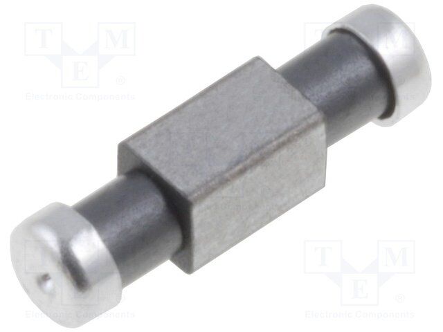
| 描述 | FILTER LC HIGH FREQ 3300PF 2706馈通电容器 3300pF 100V 2A FILT |
| ESD保护 | 无 |
| 产品分类 | |
| 品牌 | Murata Electronics |
| 产品手册 | |
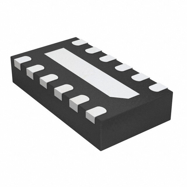
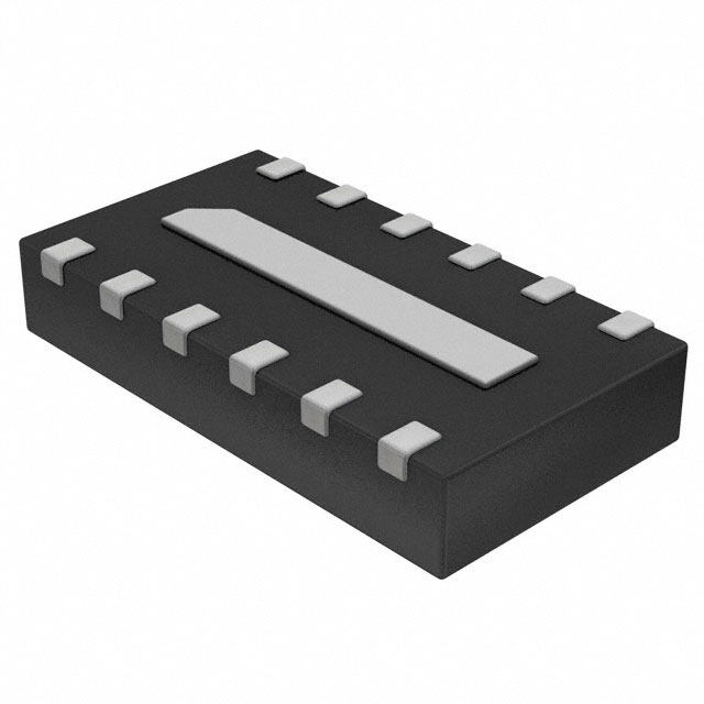
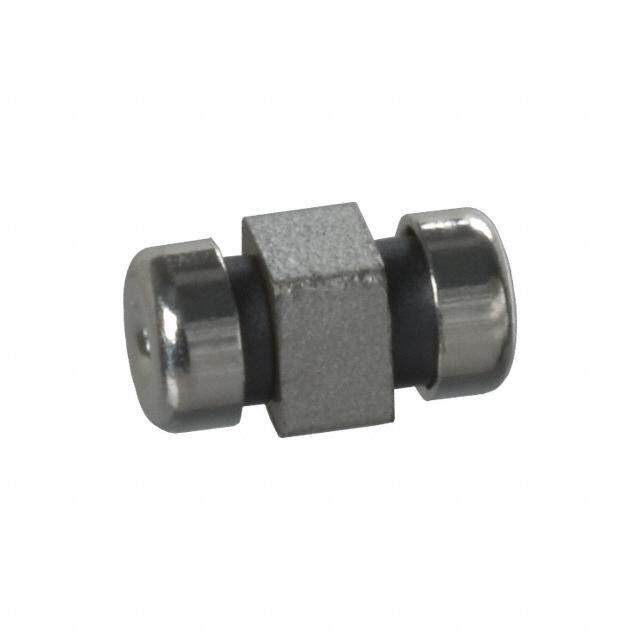
| 产品图片 |
|
| rohs | 符合RoHS无铅 / 符合限制有害物质指令(RoHS)规范要求 |
| 产品系列 | 馈通电容器,Murata Electronics NFE61HT332Z2A9LEMIFIL®, NFE61H |
| 数据手册 | |
| 产品型号 | NFE61HT332Z2A9L |
| 中心/截止频率 | - |
| 产品 | Three Terminal Filter Capacitors |
| 产品种类 | 馈通电容器 |
| 其它名称 | 490-6951-6 |
| 包装 | Digi-Reel® |
| 商标 | Murata Electronics |
| 外壳宽度 | 1.6 mm |
| 外壳长度 | 6.8 mm |
| 外壳高度 | 1.6 mm |
| 大小/尺寸 | 0.268" 长 x 0.063" 宽(6.80mm x 1.60mm) |
| 容差 | - 20 %, + 80 % |
| 封装 | Reel |
| 封装/外壳 | 2706(6816 公制),3 PC 板 |
| 封装/箱体 | 2606 (6816 metric) |
| 工作温度 | -55°C ~ 125°C |
| 工作温度范围 | - 55 C to + 125 C |
| 工厂包装数量 | 2500 |
| 应用 | 自动 |
| 技术 | LC(T 型) |
| 接地端子 | 2.6 mm |
| 数值 | C = 3300pF |
| 最大工作温度 | + 125 C |
| 最小工作温度 | - 55 C |
| 标准包装 | 1 |
| 滤波器阶数 | 2nd |
| 电压额定值 | 100 VDC |
| 电压额定值DC | 100 V |
| 电容 | 3300 pF |
| 电流 | 2A |
| 电流额定值 | 2 A |
| 电阻-通道(Ω) | - |
| 端接类型 | SMD/SMT |
| 类型 | Automotive Chip Capacitor Block LC Combined Type Feedthrough Capacitor and Ferrite Beads |
| 绝缘电阻 | 1000 MOhms |
| 衰减值 | - |
| 通道数 | 1 |
| 频率范围 | - |
| 高度 | 0.075"(1.90mm) |


- 商务部:美国ITC正式对集成电路等产品启动337调查
- 曝三星4nm工艺存在良率问题 高通将骁龙8 Gen1或转产台积电
- 太阳诱电将投资9.5亿元在常州建新厂生产MLCC 预计2023年完工
- 英特尔发布欧洲新工厂建设计划 深化IDM 2.0 战略
- 台积电先进制程称霸业界 有大客户加持明年业绩稳了
- 达到5530亿美元!SIA预计今年全球半导体销售额将创下新高
- 英特尔拟将自动驾驶子公司Mobileye上市 估值或超500亿美元
- 三星加码芯片和SET,合并消费电子和移动部门,撤换高东真等 CEO
- 三星电子宣布重大人事变动 还合并消费电子和移动部门
- 海关总署:前11个月进口集成电路产品价值2.52万亿元 增长14.8%

PDF Datasheet 数据手册内容提取
Reference Only Reference Spec. No. JENF243E-9101B-01 P 1 / 10 Chip EMIFIL ® LC Combined Type for Large Current NFE61HT□□□□2A9□ Reference Specification [AEC-Q200] 1. Scope This reference specification applies to Chip EMIFIL ® LC Combined Type for Large Current NFE61H Series for Automotive Electronics based on AEC-Q200. 2. Part Numbering NF E 61 HT 101 Z 2A 9 L Product ID Structure Dimension Features Capacitance Characteristics Rated Electrode Packaging (L× W) Voltage Code (L: Taping / B: Bulk) 3. Rating Customer Murata Rated Withstanding Rated Insulation ESD Rank Capacitance Part Number Part Number Voltage Voltage Current Resistance 2:2kV NFE61HT330U2A9L 33pF ± 30% NFE61HT330U2A9B NFE61HT680R2A9L 68pF ± 30% NFE61HT680R2A9B NFE61HT101Z2A9L 100pF ± 30% NFE61HT101Z2A9B NFE61HT181C2A9L 180pF ± 30% NFE61HT181C2A9B 100 V 1000 MΩ 250 V(DC) 2 A(DC) 2 NFE61HT361C2A9L (DC) min. 360pF ± 20% NFE61HT361C2A9B NFE61HT681D2A9L 680pF ± 30% NFE61HT681D2A9B NFE61HT102F2A9L 1000pF ± 80 % NFE61HT102F2A9B 20 NFE61HT332Z2A9L 3300pF ± 80 % NFE61HT332Z2A9B 20 • Operating Temperature: - 55 °C to + 125 °C • Storage Temperature: - 55 °C to + 125 °C 4. Standard Testing Condition <Unless otherwise specified> <In case of doubt> Temperature : Ordinary Temp. 15°C to 35°C Temperature: 20°C ± 2°C Humidity : Ordinary Humidity 25 %(RH) to 85 %(RH) Humidity : 60 %(RH) to 70 %(RH) Atmospheric pressure : 86kPa to 106kPa 5. Style and Dimensions ■ Equivalent Circuit 0.7±0.2 2.6±0.3 0.7±0.2 (1) (2) (3) Input Output 3 3 0. 0. (1) (3) ± ± 1.6 1.6 GND 1.6±0.3 6.8±0.3 (2) 0.5 ∗(1),(3):NoPolarity ■ Unit Mass(Typical value) 0.062g Note : Gap and bend between ceramic capacitor(∗) and ferrite bead(∗1) may come out as illustrated below, however, these are not affect the performance, mounting and reliability of the products. 0.5max. ∗ ∗1 ∗ ∗1 0.1max. (inmm) MURATA MFG. CO., LTD.
Reference Only Reference Spec. No. JENF243E-9101B-01 P 2 / 10 ■ Insertion Loss Characteristics (I.L.) (Typ.) (50Ωsystem) 6. Marking No marking. 7. Electrical Performance No. Item Specification Test Method 7.1 Capacitance Meet item 3. Table 1 Capacitance Voltage Frequency 33,68,100 (pF) 1 to 5 V(rms) 1MHz±10% 180,360,680 1±0.2 V(rms) 1kHz±10% 1000,3300 (pF) 7.2 Insulation Meet item 3. Voltage : 100 V(DC) Resistance(I.R.) Time : 60 ± 5 seconds 7.3 Withstanding Products shall not be damaged. Test Voltage : 250 V(DC) Voltage Testing Time : 1 to 5 seconds Limit the charging current: 10mA max. 7.4 Resistance to Meet Table 2. Attenuating transient voltage of exponential Surge Voltage Table 2 function shall be applied to products on the condition. Appearance No damaged Relay 10Ω 33,68,100 within 100Ω 1 180,360 CCahpa.n ge 680 (pF) ±15% EB 0.47µF Pr2od3uct 1000 within 3300 (pF) ±30% I.R. 1000 MΩ min. EB 400V Peak Voltage : 400 V Withstanding Voltage No damaged Force Period : 1 s The number of Surges : 105 8. Q200 Requirement 8-1. Performance (based on Table 13 for Ferrite EMI SUPPRESSORS/FILTERS) AEC-Q200 Rev.D issued June. 1 2010 AEC-Q200 Murata Specification / Deviation No. Stress Test Method 3 High Temperature 1000hours at 125C Meet TABLE A after testing. Exposure Set for 24hours Table A (Storage) at room temperature, Appearance No damage then measured. Capacitance Change (33pF-100pF: 33pF to 680pF Within +/-15% at 20C 1MHz+/-10%) (180pF-3300pF: 1000pF to 3300pF Within +/-30% at 20C 1kHz+/-10%) I.R. 1000M ohm min. Withstanding Voltage No damage MURATA MFG. CO., LTD.
Reference Only Reference Spec. No. JENF243E-9101B-01 P 3 / 10 AEC-Q200 Murata Specification / Deviation No. Stress Test Method 4 Temperature 1000cycles(-55C to 125C) Meet Table B after testing. Cycling Measurement at 24±2 hours after Table B test conclusion. Appearance No damage Capacitance Change 33pF to 680pF Within +/-15% at 20C (33pF-100pF: 1MHz+/- 10%) (180pF-3300pF: 1kHz+/- 1000pF to 3300pF Within +/-30% at 20C 10%) I.R. 100M ohm min Withstanding Voltage No damage 5 Destructive Per EIA469 No defects Physical Analysis No electrical tests 7 Biased 1000hours 85C/85%RH. Meet Table B after testing. Apply Maximum rated Voltage and Humidity current. Measurement at 24+/-2 hours after test conclusion. 8 Operational Life 1000hours at 125C Meet Table B after testing. Apply Maximum rated Current. Measurement at 24+/-2 hours after test conclusion. 9 External Visual Visual inspection No abnormalities 10 Physical Meet ITEM 4 No defects Dimension (Style and Dimensions) 12 Resistance Per MIL-STD-202 Method 215 Not Applicable to Solvents 13 Mechanical Shock Per MIL-STD-202 Method 213 Meet Table A after testing. Figure 1 of Method 213. Condition F(1500g's/0.5ms/Half sine) Three times each 6 direction. 14 Vibration 5g's for 20 minutes, 12cycles each Meet Table A after testing. of 3 oritentations Osscillation Frequency : 10- 2000Hz. 15 Resistance No heating. Pre-heating: 150C+/-5C, 60s+/-5s to Soldering Heat 260C +/- degree C Meet Table A after testing. Immersion time 10s 17 ESD Per AEC-Q200-002 Meet Table C after testing. ESD Rank: Refer to Item 3. Rating. Table C Appearance No damage I.R. 1000M ohm min Withstanding Voltage No damage 18 Solderbility Per J-STD-002 Method b : Not Applicable 75% of the terminations is to be soldered. 19 Electrical Measured :Capacitance No defects Characterization MURATA MFG. CO., LTD.
Reference Only Reference Spec. No. JENF243E-9101B-01 P 4 / 10 AEC-Q200 Murata Specification / Deviation No. Stress Test Method 20 Flammability Per UL-94 Not Applicable 21 Board Flex Epoxy-PCB(1.6mm) Meet Table D after testing. Deflection 2mm(min) Table D 60s minimum holding time Capacitance Change 33pF to 680pF Within +/-15% at 20C (33pF-100pF: 1MHz+/- 10%) (180pF-3300pF: 1kHz+/- 1000pF to 3300pF Within +/-30% at 20C 10%) 22 Terminal Strength Per AEC-Q200-006 17.7N for 60sec A force of 17.7N No defects for 60sec 30 Electrical Per ISO-7637-2 Not Applicable Transient Conduction 10. Specification of Packaging 10.1. Appearance and Dimensions (12mm-wide plastic tape) Sprocket Hole φ1.5+0.1 Embossed Cavity 0.3±0.1 -0 1 5. 70 1.± 5 0 . 0 3 0.1 5.5± 0±0. Dimension of the Cavity is .2± 12. measured at the bottom side. 7 4.0±0.1 4.0±0.1 1.9±0.1 1.75±0.1 2.0±0.05 Direction of feed (in mm) 10.2. Specification of Taping (1) Packing quantity (standard quantity) 2500 pcs. / reel (2) Packing Method Products shall be packaged in the cavity of the plastic tape and sealed with cover tape. (3) Sprocket Hole The sprocket holes are to the right as the tape is pulled toward the user. (4) Spliced point The cover tape have no spliced point. (5) Missing components number Missing components number within 0.1% of the number per reel or 1 pc., whichever is greater, and are not continuous. The specified quantity per reel is kept. 10.3. Pull Strength of Plastic Tape and Cover Tape Plastic tape 5N min. Cover tape 10N min. 10.4. Peeling off force of cover tape 165° ~180° F CoverTape 0.2N to 0.7N (minimum value is typical) ∗ Speed of Peeling off : 300 mm / min PlasticTape MURATA MFG. CO., LTD.
Reference Only Reference Spec. No. JENF243E-9101B-01 P 5 / 10 10.5. Dimensions of Leader-tape, Trailer and Reel There shall be leader-tape (cover tape only and empty tape) and trailer-tape (empty tape) as follows. Trailer Leader 2.0±0.5 160min. Label 190min. 210min. Emptytape Covertape φ13.0±0.2 φ60±10 φ21.0±0.8 Directionoffeed 13±1 0 17±1.4 φ180±0 (in: mm) 3 10.6. Marking for reel Customer part number , MURATA part number , Inspection number(∗1) , RoHS marking(∗2) , Quantity , etc ∗1) « Expression of Inspection No. » □□ OOOO ××× (1) (2) (3) (1) Factory Code (2) Date First digit : Year / Last digit of year Second digit : Month / Jan. to Sep. → 1 to 9, Oct. to Dec. → O, N, D Third, Fourth digit : Day (3) Serial No. ∗2) « Expression of RoHS marking » ROHS – Y (△) (1) (2) (1) RoHS regulation conformity parts. (2) MURATA classification number 10.7. Marking for Outside package (corrugated paper box) Customer name , Purchasing Order Number , Customer Part Number , MURATA part number , RoHS marking (∗2) , Quantity , etc 10.8. Specification of Outer Case Outer Case Dimensions Label Standard Reel Quantity in Outer Case (mm) (Reel) H W D H 186 186 93 4 D ∗ Above Outer Case size is typical. It depends on a quantity of an order. W MURATA MFG. CO., LTD.
Reference Only Reference Spec. No. JENF243E-9101B-01 P 6 / 10 11. Standard Land Dimensions The chip EMI filter suppresses noise by conducting the high-frequency noise element to ground. Therefore, to get enough noise reduction, feed through holes which is connected to ground-plane should be arranged according to the figure to reinforce the ground-pattern. (a) Standard land dimensions for reflow (b) Standard land dimensions for flow (But, NFE61HT332Z2A9□ is not applicable.) ・Side on which chips are mounted ・Side on which chips are mounted Smalldiameterthruholeφ0.4 Smalldiameterthruholeφ0.4 6 6 0 62 26 1. 2. 3. 0.1. 3.3. 2.0 Resist 1.5 3.8 Resist 4.8 Copperfoilpattern 4.8 Copperfoilpattern 8.8 Nopattern 9.0 Nopattern (inmm) 12. ! Caution 12.1. Limitation of Applications Please contact us before using our products for the applications listed below which require especially high reliability for the prevention of defects which might directly cause damage to the third party’s life, body or property. (1)Aircraft equipment (2)Aerospace equipment (3)Undersea equipment (4)Power plant control equipment (5)Medical equipment (6)Transportation equipment( trains, ships, etc.) (7)Traffic signal equipment (8)Disaster prevention / crime prevention equipment (9)Data-processing equipment (10)Applications of similar complexity or with reliability requirements comparable to the applications listed in the above 12.2. Fail Safe Be sure to provide an appropriate fail-safe function on your product to prevent from a second damage that may be caused by the abnormal function or the failure of our products. 13.Notice This product is designed for solder mounting. Please consult us in advance for applying other mounting method such as conductive adhesive. 13.1. Flux and Solder Flux Use rosin-based flux, Do not use highly acidic flux (with chlorine content exceeding 0.2(wt)%). Do not use water-soluble flux. Solder Use Sn-3.0Ag-0.5Cu solder 13.2. Note for Assembling < Thermal Shock > Pre-heating should be in such a way that the temperature difference between solder and products surface is limited to 100°C max. Also cooling into solvent after soldering should be in such a way that the temperature difference is limited to 100°C max. <Consideration for mounting of 2.5mm pitch> The mounting of 2.5mm pitch should be prevented on flow soldering to avoid an excess of solder volume. < Exclusive Use of Reflow Soldering > NFE61HT332Z2A9□ can only be soldered with reflow. If it were soldered with flow, cracks might be caused in the ceramic body. So, reflow soldering shall be applied for products. 13.3. Attention Regarding P.C.B. Bending The following shall be considered when designing P.C.B.'s and laying out products. MURATA MFG. CO., LTD.
Reference Only Reference Spec. No. JENF243E-9101B-01 P 7 / 10 (1) P.C.B. shall be designed so that products are not subject to the mechanical stress for board warpage. 〔Products direction〕 a Products shall be located in the sideways direction < b (Length:a b) to the mechanical stress. 〈Poorexample〉 〈Goodexample〉 (2) Components location on P.C.B. separation. It is effective to implement the following measures, to reduce stress in separating the board. It is best to implement all of the following three measures; however, implement as many measures as possible to reduce stress. Contents of Measures Stress Level (1) Turn the mounting direction of the component parallel to the board separation surface. A > D *1 (2) Add slits in the board separation part. A > B (3) Keep the mounting position of the component away from the board separation surface. A > C *1 A > D is valid when stress is added vertically to the perforation as with Hand Separation.If a Cutting Disc is used, stress will be diagonal to the PCB, therefore A > D is invalid. (3) Mounting Components Near Screw Holes When a component is mounted near a screw hole, it may be affected by the board deflection that occurs during the tightening of the screw. Mount the component in a position as far away from the screw holes as possible. 13.4. Standard Soldering Conditions On flow soldering (e.g. double wave soldering), use the product in consideration of the conditions of solder, solder temperature and immersion time (melting time) because longer soldering time may cause the corrosion of the electrode. On dipping soldering, use the product in consideration of the conditions of solder, solder temperature, flux, preheat and so on because de-wetting may be caused. Standard soldering profile and the limit soldering profile is as follows. The excessive soldering conditions may cause leaching of the electrode and/or resulting in the deterioration of product quality. MURATA MFG. CO., LTD.
Reference Only Reference Spec. No. JENF243E-9101B-01 P 8 / 10 < Flow Soldering Profile > Temp. (°C) 265°C±3°C 250°C Limit Profile 150 HeatingTime StandardProfile 60smin. Time.(s) Standard Profile Limit Profile Pre-heating 150°C , 60s min. Heating 250°C , 4s ~ 6s 265°C ± 3°C , 5s max. Cycle of flow 2 times 2 times < Reflow Soldering Profile > Temp. 260°C (°C) 245°C±3°C 230°C 220°C Limit Profile 180 150 30s~60s StandardProfile 60smax. 90s±30s Time.(s) Standard Profile Limit Profile Pre-heating 150°C ~ 180°C , 90s ± 30s Heating above 220°C , 30s ~ 60s above 230°C , 60s max. Peak temperature 245°C ± 3°C 260°C , 10s Cycle of reflow 2 times 2 times 13.5. Printing of Adhesive (Flow Soldering) Adhesive amount shall be about 0.5mg for one position to obtain enough adhesive strength. The adhesive position is as follows. 0.6 1.2 3.2 1.5 4.8 Adhesive 9.0 Positionofadhesive (inmm) 13.6. Solder paste printing for reflow • Standard printing pattern of solder paste. · Standard thickness of the solder paste should be 150μm to 200µm. 6 6 · Use the solder paste printing pattern of the right pattern. 1. 2. · For the resist and copper foil pattern, use standard land dimensions. 1.5 4.8 8.8 (inmm) MURATA MFG. CO., LTD.
Reference Only Reference Spec. No. JENF243E-9101B-01 P 9 / 10 13.7. Reworking with Soldering iron The following conditions shall be strictly followed when using a soldering iron. • Pre-heating : 150°C, 1 min • Soldering iron output : 30W max. • Tip temperature : 350°C max. • Tip diameter : φ3mm max. • Soldering time : 3(+1,-0) s • Times : 2times max. Note: Do not directly touch the products with the tip of the soldering iron in order to prevent the crack on the ceramic material due to the thermal shock. 13.8. Cleaning Conditions Products shall be cleaned on the following conditions. (1) Cleaning temperature shall be limited to 60°C max. (40°C max. for IPA.) (2) Ultrasonic cleaning shall comply with the following conditions, with avoiding the resonance phenomenon at the mounted products and P.C.B. Power: 20W / l max. Frequency: 28kHz to 40kHz Time: 5 minutes max. (3) Cleaner 1. Cleaner · Isopropyl alcohol (IPA) 2. Aqueous agent · PINE ALPHA ST-100S (4) There shall be no residual flux and residual cleaner after cleaning. In the case of using aqueous agent, products shall be dried completely after rinse with de-ionized water in order to remove the cleaner. (5) Other cleaning Please contact us. 13.9. Operating Environment Do not use this product under the following environmental conditions, on deterioration of the performance, such as insulation resistance may result from the use. (1) in the corrodible atmosphere (acidic gases, alkaline gases, chlorine, sulfur gases, organic gases and etc.) (2) in the atmosphere where liquid such as organic solvent, may splash on the products. 13.10. Resin coating It may affect on the product's performance when using resin for coating / molding products. So please pay your careful attention when you select resin. In prior to use, please make the reliability evaluation with the product mounted in your application set. 13.11. Handling of a substrate After mounting products on a substrate, do not apply any stress to the product caused by bending or twisting to the substrate when cropping the substrate, inserting and removing a connector from the substrate or tightening screw to the substrate. Excessive mechanical stress may cause cracking in the product. Bending Twisting 13.12. Storage condition (1) Storage period Use the products within 12 months after delivered. Solderability should be checked if this period is exceeded. (2) Storage environment condition · Products should be stored in the warehouse on the following conditions. Temperature : - 10 °C to + 40 °C Humidity : 15 % to 85% relative humidity No rapid change on temperature and humidity · Don't keep products in corrosive gases such as sulfur, chlorine gas or acid, or it may cause oxidization of electrode, resulting in poor solderability. · Products should be stored on the palette for the prevention of the influence from humidity, dust and so on. · Products should be stored in the warehouse without heat shock, vibration, direct sunlight and so on. · Products should be stored under the airtight packaged condition. (3) Delivery Care should be taken when transporting or handling product to avoid excessive vibration or mechanical shock. MURATA MFG. CO., LTD.
Reference Only Reference Spec. No. JENF243E-9101B-01 P 10 / 10 14. ! Notes (1)Please make sure that your product has been evaluated in view of your specifications with our product being mounted to your product. (2)You are requested not to use our product deviating from the agreed specifications. (3)The contents of this reference specification are subject to change without advance notice. Please approve our product specifications or transact the approval sheet for product specifications before ordering. MURATA MFG. CO., LTD.