ICGOO在线商城 > 滤波器 > EMI/RFI 滤波器(LC,RC 网络) > BNX022-01L
 Datasheet下载
- 型号: BNX022-01L
- 制造商: Murata
- 库位|库存: xxxx|xxxx
- 要求:
| 数量阶梯 | 香港交货 | 国内含税 |
| +xxxx | $xxxx | ¥xxxx |
查看当月历史价格
查看今年历史价格
BNX022-01L产品简介:
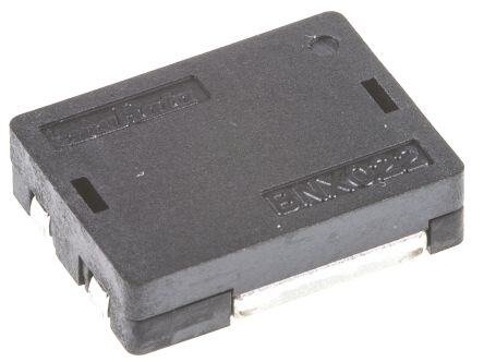
ICGOO电子元器件商城为您提供BNX022-01L由Murata设计生产,在icgoo商城现货销售,并且可以通过原厂、代理商等渠道进行代购。 BNX022-01L价格参考¥25.40-¥25.40。MurataBNX022-01L封装/规格:EMI/RFI 滤波器(LC,RC 网络), LC EMI Filter 5th Order Low Pass 2 Channel C = 1µF 20A 4-SMD, No Lead。您可以下载BNX022-01L参考资料、Datasheet数据手册功能说明书,资料中有BNX022-01L 详细功能的应用电路图电压和使用方法及教程。
Murata Electronics North America 生产的型号为 BNX022-01L 的 EMI/RFI 滤波器(LC,RC 网络)主要用于抑制和过滤电子设备中的电磁干扰 (EMI) 和射频干扰 (RFI),确保设备在复杂电磁环境中稳定运行。以下是该滤波器的一些应用场景:

1. 消费电子产品:如智能手机、平板电脑、笔记本电脑等便携式设备中,BNX022-01L 可以有效减少内部电路之间的干扰,提高信号质量和稳定性,延长电池寿命,并确保设备符合国际电磁兼容性 (EMC) 标准。

2. 汽车电子系统:在现代汽车中,各种电子控制系统(如发动机控制单元、车身控制模块、娱乐系统等)会产生大量电磁噪声。BNX022-01L 可用于这些系统的电源线和信号线上,防止干扰影响车辆的安全性和性能。

3. 工业自动化设备:工厂自动化设备(如可编程逻辑控制器 PLC、伺服驱动器、传感器等)对电磁环境要求较高。BNX022-01L 能够有效抑制来自外部或内部的电磁干扰,确保设备正常工作,避免因干扰导致的误操作或停机。

4. 通信设备:在基站、路由器、交换机等通信设备中,EMI/RFI 干扰会影响数据传输的可靠性和速度。使用 BNX022-01L 可以净化电源和信号路径,减少噪声,提升通信质量,保证网络的稳定性和安全性。

5. 医疗设备:医疗设备(如心电图机、超声波仪、CT 扫描仪等)对电磁干扰非常敏感,任何微小的干扰都可能影响诊断结果。BNX022-01L 可以确保这些设备在医院等复杂环境中稳定运行,提供准确的检测数据。

总之,BNX022-01L 适用于需要高电磁兼容性的各种电子设备,能够有效减少电磁干扰,提升设备的性能和可靠性。
| 参数 | 数值 |
| 产品目录 | |
| 描述 | FILTER EMI 10A 50V 1MHZ-1GHZ SMDEMI网络滤波器阵列 500M ohm 50volt 10A EMIFIL |
| ESD保护 | 无 |
| 产品分类 | EMI/RFI 滤波器(LC、RC 网络)EMI/RFI 器件 |
| 品牌 | Murata Electronics North America |
| 产品手册 | |
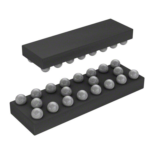
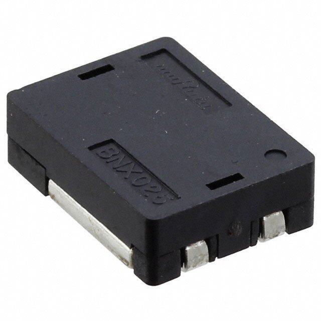
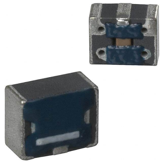
| 产品图片 |
|
| rohs | 符合RoHS无铅 / 符合限制有害物质指令(RoHS)规范要求 |
| 产品系列 | EMI网络滤波器阵列,Murata Electronics BNX022-01LEMIFIL®, BNX02 |
| 数据手册 | |
| 产品型号 | BNX022-01L |
| 中心/截止频率 | 50MHz(截止值) |
| 产品 | EMI Network Filter Arrays |
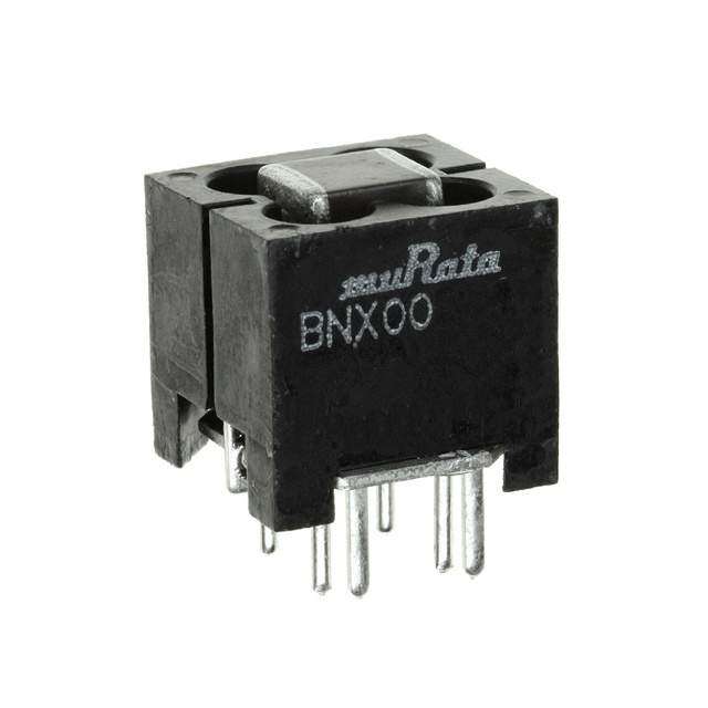
| 产品目录绘图 |
|
| 产品目录页面 | |
| 产品种类 | EMI网络滤波器阵列 |
| 元件数量 | 4 |
| 其它名称 | 490-5052-6 |
| 包装 | Digi-Reel® |
| 商标 | Murata Electronics |
| 外壳宽度 | 9.1 mm |
| 外壳长度 | 12.1 mm |
| 外壳高度 | 3.1 mm |
| 大小/尺寸 | 0.476" 长 x 0.358" 宽(12.10mm x 9.10mm) |
| 封装 | Reel |
| 封装/外壳 | 4-SMD,无引线 |
| 工作温度 | -40°C ~ 125°C |
| 工作温度范围 | - 40 C to + 125 C |
| 工厂包装数量 | 400 |
| 应用 | 通用 |
| 截止频率 | - |
| 技术 | LC |
| 数值 | - |
| 标准包装 | 1 |
| 滤波器阶数 | 5th |
| 特色产品 | http://www.digikey.com/cn/zh/ph/Murata/BNX.html |
| 电容 | - |
| 电感 | - |
| 电流 | 10A |
| 电路类型 | LC Filter |
| 电阻 | - |
| 电阻-通道(Ω) | - |
| 端接类型 | SMD/SMT |
| 类型 | 低通 |
| 衰减值 | 35dB @ 1MHz ~ 1GHz |
| 通道数 | 2 |
| 通道数量 | 2 Channel |
| 频率范围 | 1 MHz to 1 GHz |
| 高度 | 0.130"(3.30mm) |


- 商务部:美国ITC正式对集成电路等产品启动337调查
- 曝三星4nm工艺存在良率问题 高通将骁龙8 Gen1或转产台积电
- 太阳诱电将投资9.5亿元在常州建新厂生产MLCC 预计2023年完工
- 英特尔发布欧洲新工厂建设计划 深化IDM 2.0 战略
- 台积电先进制程称霸业界 有大客户加持明年业绩稳了
- 达到5530亿美元!SIA预计今年全球半导体销售额将创下新高
- 英特尔拟将自动驾驶子公司Mobileye上市 估值或超500亿美元
- 三星加码芯片和SET,合并消费电子和移动部门,撤换高东真等 CEO
- 三星电子宣布重大人事变动 还合并消费电子和移动部门
- 海关总署:前11个月进口集成电路产品价值2.52万亿元 增长14.8%


PDF Datasheet 数据手册内容提取
Reference Only Spec.No. JENF243H-0008M-01 P 1/ 14 SMD Block Type EMIFIL ® BNX02□-01□ Reference Specification 1.Scope This reference specification applies to SMD Block Type EMIFIL®. 2.Part Numbering BN X 022 -01 L Product ID Type Serial No. Features Packaging Code (L :Taping(φ178mm reel) / K :Taping(φ330mm reel) / B :Bulk) 3.Rating Rated Customer’s Rated Withstanding DC Insulation Voltage Part Number Capacitance Current Insertion Loss Part Number Voltage Voltage Resistance Resistance Drop ∗ BNX022-01L 35dB min. 50V 125V 20A 0.43mΩ 500MΩ 30 mV BNX022-01K 1.0µF±15% (1MHz to (DC) (DC) (DC) ±0.20mΩ min. max. BNX022-01B 1GHz) BNX023-01L 35dB min. 100V 250V 20A 0.43mΩ 500MΩ 45mV BNX023-01K 1.0µF±15% (1MHz to (DC) (DC) (DC) ±0.20mΩ min. max. BNX023-01B 1GHz) BNX028-01L 35dB min. 20 16V 40V 20A 0.43mΩ 1.1MΩ 45mV BNX028-01K 47μF± % (30KHz~ 50 (DC) (DC) (DC) ±0.20mΩ min. max. BNX028-01B 1GHz) BNX029-01L 35dB min. 20 6.3V 15.8V 20A 0.43mΩ 0.5MΩ 45mV BNX029-01K 100μF± % (15KHz~ 50 (DC) (DC) (DC) ±0.20mΩ min. max. BNX029-01B 1GHz) ∗ Rated current is derated according to operating temperature. BNX022-01 BNX023-01 BNX029-01 BNX028-01 A) (A) Current( 2105 dCurrent 2105 ated Rate R 1 1 85 125 6855 110255 OperatingTemperature(°C) OperatingTemperature(°C) • Operating Temperature : - 40 °C to + 125 °C (BNX022-01/ BNX023-01/ BNX029-01) - 40 °C to + 105 °C (BNX028-01) • Storage Temperature : - 55 °C to + 125 °C 4.Standard Testing Condition <Unless otherwise specified> <In case of doubt> Temperature : Ordinary Temp. 15 °C to 35 ºC Temperature : 20 °C ± 2 °C Humidity : Ordinary Humidity 25 %(RH) to 85 %(RH) Humidity : 60 %(RH) to 70 %(RH) Atmospheric pressure : 86kPa to 106kPa MURATA MFG.CO.,LTD.
Reference Only Spec.No. JENF243H-0008M-01 P 2/ 14 5.Style and Dimensions ※Coplanarity 0.10mm max ■Equivalent Circuit L1 L3 C2 ① ② ①B :Bias ②CB :Circuit + Bias L2 C1 ③PSG :Power Supply Ground ④CG :Circuit Ground ③ ④ ■ Unit Mass (Typical value) 0.80g 6.Marking Filter shall be marked as follows. (1) Murata Mark : (2) Part Number : BNX022-01:( BNX022 ) BNX023-01:( BNX023 ) BNX028-01:( BNX028 ) BNX029-01:( BNX029 ) (3) Polarity Marking : ○ MURATA MFG.CO.,LTD.
Reference Only Spec.No. JENF243H-0008M-01 P 3/ 14 7.Electrical Performance No. Item Specification Test Method 7.1 Insertion Meet item 3. 50Ω 50Ω Loss 10dB Balun (1) (2) 10dB Attenuator Specimen Attenuator 50Ω (3) (4) E ~ 50Ω SG ∗MethodofmeasurementbasedonMIL-STD-220 Insertion Loss = -20 log E1/E0 (dB) E0 : Level without FILTER (short) E1: Level with FILTER 7.2 Capacitance Measured by the following condition between Terminal ①② and ③④. (see item 5.) Frequency : 1 ± 0.1kHz(BNX022/BNX023) 120±24Hz (BNX028/BNX029) Voltage : 1 V(rms) max. (BNX022/BNX023) 0.5±0.1V(rms). (BNX028/BNX029) Measuring Equipment : Agilent4278A or the equivalent(BNX022/BNX023) Agilent4284A or the equivalent(BNX028/BNX029) 7.3 DC Measured by the way of 4 terminal method between Resistance ① and ② and between ③ and ④. (see item 5.) 7.4 Insulation Measured at DC rated voltage between terminal Resistance ①② and ③④. (see item 5.) Time : 60 s max Charging current : 50 mA max. Measuring Equipment : R8340A or the equivalent 7.5 Withstanding Filter shall be no failure. Withstanding voltage shall be applied between Voltage terminal ①② and ③④. (see item 5.) Test Voltage : BNX022-01 125V(DC) BNX023-01 250 V(DC) BNX028-01 40 V(DC) BNX029-01 15.8 V(DC) Time : 5 ± 1 s Charging current : 50 mA max. 7.6 Voltage Meet item 3. After soldering the part on the test substrate, Drop measure the voltage with passing the rated current as shown in the schematic below. A (1) V Specimen (2) Where the terminals of the part shall be connected as follows: Referring to the terminal No. shown in item 5, connect terminal No. ② and ④ by soldering copper wire with diameter more than 1mm / length less than 6mm. Then connect terminal No. ① as (1) and terminal No. ③ as (2) the measurement circuit as mentioned above. The probe for measuring the voltage shall be touched on the solder fillet of ①③. MURATA MFG.CO.,LTD.
Reference Only Spec.No. JENF243H-0008M-01 P 4/ 14 8.Mechanical Performance No. Item Specification Test Method 8.1 Appearance and Meet item 5. Visual Inspection and measured with Micrometer Dimensions caliper and Slide Caliper. 8.2 Marking Meet item 5. Visual Inspection 8.3 Reflow Appropriate solder fillet is formed. It shall be soldered with the Standard Profile condition as Solderability shown No.13.6(2) Soldering Condition. ・thickness of solder paste : 150 to 200 µm ・Land dimension : see No.13.5. 8.4 Resistance to Meet Table 1. Soldering iron : 100 W max. soldering iron Tip Temperature : 450 °C ± 5 °C Table 1 Soldering Time : 5 s , 2 Times Appearance No damaged Do not touch the products directly with the tip of the Cap.Change BNX022 within soldering iron. BNX023 ±7.5% BNX028 within <About BNX028,BNX029> BNX029 ±15% · Initial values: measured after heat treatment (150± 010 °C, I.R. meet item 3 1hour) and exposure in the room condition for 24±2 hours. Dielectric ·Values After Testing:measured after heat treatment (150± Strength No failure 010 °C, 1hour) and exposure in the room condition for 24±2 hours. 8.5 Bending It shall be soldered on the glass-epoxy substrate. Strength (100mm×40mm×1.6mm) Pressurejig R230 F Deflection 45 45 Product Deflection : 2 mm Keeping Time : 30 s Speed : 0.5 mm/s <About BNX028,BNX029> · Initial values: measured after heat treatment (150± 010 °C, 1hour) and exposure in the room condition for 24±2 hours. ·Values After Testing:measured after heat treatment (150± 010 °C, 1hour) and exposure in the room condition for 24±2 hours. 8.6 Drop Meet Table 2. It shall be dropped on concrete or steel board. Method : free fall Table 2 Height : 1 m Appearance No damaged The Number of Time : 10 times Cap.Change within ±15% I.R. meet item 3 <About BNX028,BNX029> Dielectric No failure · Initial values: measured after heat treatment (150± 010 °C, Strength 1hour) and exposure in the room condition for 24±2 hours. ·Values After Testing:measured after heat treatment (150± 010 °C, 1hour) and exposure in the room condition for 24±2 hours. MURATA MFG.CO.,LTD.
Reference Only Spec.No. JENF243H-0008M-01 P 5/ 14 No. Item Specification Test Method 8.7 Vibration Meet Table 2. It shall be soldered on the glass-epoxy substrate. Oscillation Frequency : 10 to 2000 to 10Hz for 20 minutes Total amplitude 3.0 mm or Acceleration amplitude 196 m/s2 whichever is smaller. Time : A period of 3 hours in each of 3 mutually perpendicular directions. (Total 9 hours) <About BNX028,BNX029> · Initial values: measured after heat treatment (150± 010 °C, 1hour) and exposure in the room condition for 24±2 hours. ·Values After Testing:measured after heat treatment (150± 010 °C, 1hour) and exposure in the room condition for 24±2 hours. 8.8 Shock It shall be soldered on the glass-epoxy substrate. Acceleration : 14700 m/s2 Normal duration: 0.5 ms Waveform : Half-sine wave Direction : 6 direction Testing Time : 3 times for each direction <About BNX028,BNX029> · Initial values: measured after heat treatment (150± 010 °C, 1hour) and exposure in the room condition for 24±2 hours. ·Values After Testing:measured after heat treatment (150± 010 °C, 1hour) and exposure in the room condition for 24±2 hours. 9.Environmental Performance (It shall be soldeared on the substrate.) No. Item Specification Test Method 9.1 Heat BNX022/BNX023:Meet Table 1. 1 Cycle Shock BNX028/BNX029:Meet Table 3. 1 step : -55°C(+0°C,-3°C) / 30 min. (+3,-0) min. 2 step : Room Temperature / within 0.5 min. 3 step : 125(+3°C,-0°C) / 30 min. (+3,-0) min. (for BNX028: 105(+3°C,-0°C) / 30 min. (+3,-0) min.) 4 step : Room Temperature / within 0.5 min. Total cycles BNX022 1000cycles BNX023 100cycles BNX028 BNX029 Then measure values after exposure in the room condition for 48 ± 4 hours. <About BNX028,BNX029> · Initial values: measured after heat treatment (150± 010 °C, 1hour) and exposure in the room condition for 24±2 hours. ·Values After Testing:measured after heat treatment (150± 010 °C, 1hour) and exposure in the room condition for 24±2 hours. MURATA MFG.CO.,LTD.
Reference Only Spec.No. JENF243H-0008M-01 P 6/ 14 No. Item Specification Test Method 9.2 Humidity Meet Table 3. Temperature : 60 ± 2 °C Life Table 3 Humidity : 90 ∼ 95 %(RH) ① Voltage : Rated Voltage Appearance No damaged Time : 1000 h (+ 48h , - 0h) Cap.Change BNX022 within Then measure values after exposure in the room condition BNX023 ±12.5% for 48 ± 4 hours. BNX028 within BNX029 ±15% <About BNX028,BNX029> I.R. BNX022 25MΩ BNX023 min. · Initial values: measured after heat treatment (150± 010 °C, BNX028 0.11MΩ 1hour) and exposure in the room condition for 24±2 hours. min. ·Values After Testing:measured after heat treatment (150± BNX029 0.05MΩ 010 °C, 1hour) and exposure in the room condition for 24±2 min. hours. Humidity Temperature : 85 ± 2 °C Life Humidity : 80 ∼ 85 %(RH) ② Voltage : Rated Voltage Time : 1000 h (+ 48h , - 0h) Then measure values after exposure in the room condition for 48 ± 4 hours. <About BNX028,BNX029> · Initial values: measured after heat treatment (150± 010 °C, 1hour) and exposure in the room condition for 24±2 hours. ·Values After Testing:measured after heat treatment (150± 010 °C, 1hour) and exposure in the room condition for 24±2 hours. 9.3 Heat Life Meet Table 4. Temperature : 125 ± 2 °C Table 4 Voltage : Rated Voltage × 2 Appearance No damaged Time : 1000 h (+ 48h , - 0h) Cap.Change BNX022 within Then measure values after exposure in the room condition BNX023 ±12.5% for 48 ± 4 hours. BNX028 within BNX029 ±15% <About BNX028,BNX029> I.R. BNX022 50MΩ · Initial values: measured after heat treatment (150± 010 °C, BNX023 min. 1hour) and exposure in the room condition for 24±2 hours. BNX028 0.11MΩ ·Values After Testing:measured after heat treatment (150± min. 010 °C, 1hour) and exposure in the room condition for 24±2 BNX029 0.05MΩ hours. min. MURATA MFG.CO.,LTD.
Reference Only Spec.No. JENF243H-0008M-01 P 7/ 14 10.Insertion Loss Characteristics (I.L.) (Typ.) BNX022-01/BNX023-01 BNX028-01 BNX029-01 11. Specification of Packaging 11.1 Appearance and Dimensions (24mm-wide plastic tape) (1) plastic tape 4.0×10pich=40.0±0.2 2.0±0.1 Cavity SprocketHole 4.0±0.1 0.1 0.5 1 φ1.5±0 φ1.5±0 ±0. 0.3±0.1 5 7 1. 1 2.4±0.1 11.5±0. 24.0±0.2 1 3.3±0.1 9.4±0.1 12.0±0.1 T Directionoffeed T:3.5± 0(.1in(:mBNmX)022/BNX023) 3.6±0.1(BNX028/BNX029) (in:mm) *Dimension of the Cavity is measured at the bottom side. MURATA MFG.CO.,LTD.
Reference Only Spec.No. JENF243H-0008M-01 P 8/ 14 (2)Direction of the product 022 022 022 X X X BN BN BN MURATA logo mark 11.2 Specification of Taping (1) Packing quantity (standard quantity) φ178mm reel : 400 pcs. / reel φ330mm reel : 1500 pcs. / reel (2) Packing Method Products shall be packaged in the cavity of the plastic tape and sealed with cover tape. (3) Spliced point The cover tape have no spliced point. (4) Sprocket Hole The sprocket holes are to the right as the tape is pulled toward the user. (5) Missing components number Missing components number within 0.1% of the number per reel or 1 pc., whichever is greater, and are not continuous. The specified quantity per reel is kept. 11.3 Pull Strength of Plastic Tape and Cover Tape Plastic tape 10N min. 165to180degree Cover tape F Covertape 11.4 Peeling off force of Cover tape 0.2N to 0.7N (minimum value is typical) Plastictape ∗ Speed of Peeling off : 300 mm / min MURATA MFG.CO.,LTD.
Reference Only Spec.No. JENF243H-0008M-01 P 9/ 14 11.5 Dimensions of Leader-tape, Trailer and Reel There shall be leader-tape (top tape and empty tape) and trailer-tape (empty tape) as follows. [ Packaging Code:L (φ178mm reel) ] Trailer Leader 160min. 2.0±0.5 Label 190min. 210min. Emptytape Covertape φ62± φ13.0±0.2 0.5 φ21.0±0.8 Directionof feed 2.2±0.1 24.8~26.5 φ178±0.5 (in:mm) [ Packaging Code:K (φ330mm reel) ] Trailer Leader 2.0±0.5 160min. Label 190min. 210min. Emptytape Covertape φ100± φ13.0±0.2 1.0 φ21.0±0.8 Directionof feed 2±0.2 25.5±0.5 φ330±2.0 (in:mm) 11.6 Marking for reel Customer part number, MURATA part number, Inspection number(∗1), RoHS marking (∗2), Quantity, etc ∗1) « Expression of Inspection No. » □□ OOOO ××× (1) (2) (3) (1) Factory Code (2) Date First digit : Year / Last digit of year Second digit : Month / Jan. to Sep. → 1 to 9, Oct. to Dec. → O,N,D Third, Fourth digit : Day (3) Serial No. ∗2) « Expression of RoHS marking » ROHS – Y (△) (1) (2) (1) RoHS regulation conformity parts. (2) MURATA classification number MURATA MFG.CO.,LTD.
Reference Only Spec.No. JENF243H-0008M-01 P 10/ 14 11.7 Marking for Outside package (corrugated paper box) Customer name, Purchasing Order Number, Customer Part Number, MURATA part number, RoHS discrimination(∗2) , Quantity , etc 11.8 Specification of Outer Case Label Outer Case Dimensions Standard Reel Quantity Reel (mm) H in Outer Case (Reel) W D H D φ178mm 186 186 93 3 W φ330mm 340 340 85 2 ∗ Above Outer Case size is typical. It depends on a quantity of an order. 12. ! Caution 12.1.Direction of mounting Please make sure of the direction of mounting and connect to the circuit properly. As shown in the equivalent circuit shown in item 5, this product has a directionality. Wrong connection to the circuit may cause open/short circuit of the part, burnout and serious accidents. 12.2.Limitation of Applications Please contact us before using our products for the applications listed below which require especially high reliability for the prevention of defects which might directly cause damage to the third party’s life,body or property. (1)Aircraft equipment (2)Aerospace equipment (3)Undersea equipment (4)Power plant control equipment (5)Medical equipment (6)Transportation equipment(automobiles,trains,ships,etc.) (7)Traffic signal equipment (8)Disaster prevention / crime prevention equipment (9)Data-processing equipment (10)Applications of similar complexity or with reliability requirements comparable to the applications listed in the above 12.3.ESD ESD to this product, exceeding condition of IEC61000-4-2 with 30kV, may cause short circuit and fuming or firing. 13.Notice Products can only be soldered with reflow. This product is designed for solder mounting. Please consult us in advance for applying other mounting method such as conductive adhesive. 13.1. Flux and Solder Flux Use rosin-based flux, Do not use highly acidic flux (with chlorine content exceeding 0.2(wt)%). Do not use water soluble flux. Solder Use Sn-3.0Ag-0.5Cu solder Other flux (except above) Please contact us for details, then use. 13.2. Note for Assembling <Exclusive Use of Reflow Soldering> When installing by the flow soldering, the degradation of the insulation resistance sometimes occurs. Products can only be soldered with reflow. The use in flow soldering be reserved. < Thermal Shock > Pre-heating should be in such a way that the temperature difference between solder and products surface is limited to 100 °C max. Also cooling into solvent after soldering should be in such a way that the temperature difference is limited to 100 °C max. Insufficient pre-heating may cause cracks on the ferrite, resulting in the deterioration of product quality. MURATA MFG.CO.,LTD.
Reference Only Spec.No. JENF243H-0008M-01 P 11/ 14 13.3. Attention Regarding P.C.B. Bending The following shall be considered when designing P.C.B.'s and laying out products. (1) P.C.B. shall be designed so that products are not subject to the mechanical stress for board warpage. 〔Products direction〕 a Products shall be locatedin the sideways b < direction (Length:a b) to the mechanical stress. 〈Poorexample〉 〈Goodexample〉 (2) Products location on P.C.B. near seam for separation. Products (A,B,C,D) shall be located carefully C Seam B so that products are not subjected to the mechanical stress due to warping the board. Because they may be subjecte the mechanical b A D Slit stress in order of A > C > B ≅ D. Lengh:a<b a 13.4. Attention Regarding P.C.B. Design Portionof Perforation < The Arrangement of Products > × P.C.B. shall be designed so that products are P.C.B. ○ far from the portion of perforation. ○ Product Portionof × The portion of perforation shall be designed Perforation as narrow as possible, and shall be designed so as not to be applied the stress in the case of P.C.B. separation. P.C.B. ○ × Products shall not be arranged on the line Product of a series of holes when there are big Hole holes in P.C.B. (Because the stress concentrate on the line of holes.) < Products Placing > Pickupnozzle Support pins shall be set under P.C.B . to prevent causing a warp to P.C.B. during placing the products on the other side of P.C.B. P.C.B. Supportpin < P.C.B. Separation > P.C.B. shall not be separated with hand. P.C.B. shall be separated with the fixture so as not to cause P.C.B. bending. MURATA MFG.CO.,LTD.
Reference Only Spec.No. JENF243H-0008M-01 P 12/ 14 13.5. Standard Land Dimensions 12.5 CG 10.2 9.9 9.6 B CB 7.1 6.2 5.3 PSG CG Copper foil pattern 2.8 2.3 Copper foil pattern+Resist CG 0 Etchedarea Through hole 0 3.8 5.8 10.3 13.213.7 17.5 (in:mm) (1)Design the land pads for this part as shown above on both side printed circuit board ( or a multiple layered substrate ). (2) This product is designed to meet large current. Please design PCB pattern which is connected to this product not to become too hot by applied large current. (3)Ground area of CG should be connected to ground layer on the other side (or ground layer of multiple layered substrate) with through holes as shown above. It is recommended to take the ground area as wide as possible. (4)It is recommended to use the connection to the ground layer with through holes and the ground layer to be circuit board wide. (5)Even in case that it isn't possible to use a both side printed circuit board ( or a multiple layered substrate ), the land pads for CG should be designed as wide as possible. 13.6. Reflow Soldering (1) Solder paste printing for reflow soldering · Standard thickness of solder paste should be 150 to 200 µm. Incidentally, depending on the reflow condition and the way of heat conduction, the solder would not wet up the terminal, being possible to lead to not enough connection between terminals and lands on the circuit board / open circuit in the circuit board. In case of use, always evaluate this part in your products with actual use condition. · For the solder paste printing pattern, use standard land dimensions. · For the resist and copper foil pattern, use standard land dimensions. · Use Sn / Pn = 60 / 40 or Sn-3.0Ag-0.5Cu solder MURATA MFG.CO.,LTD.
Reference Only Spec.No. JENF243H-0008M-01 P 13/ 14 (2) Soldering Conditions Standard soldering profile and the limit soldering profile is as follows. The excessive soldering conditions may cause leaching of the electrode and/or resulting in the deterioration of product quality. Temp. 260°C (°C) 245°C±3°C 230°C 220°C Limit Profile 180 150 30s~60s Standard Profile 60smax. 90s±30s Time.(s) Standard Profile Limit Profile Pre-heating 150°C~180°C, 90s ± 30s Heating above 220°C, 30s ~ 60s above 230°C, 60s max. Peak temperature 245°C±3°C 260°C, 10s Cycle of reflow 2 times 2 times 13.7. Reworking with Soldering iron · The following conditions shall be strictly followed when using a soldering iron. Pre-heating 150°C,1 min Tip temperature 450°C max. Soldering iron output 100W max. Soldering time 5s Time 2 times Note : Do not touch the products directly with the tip of the soldering iron. 13.8. Cleaning Conditions Don't cleaning product due to non-waterproof construction. 13.9. Operating Environment Do not use this product under the following environmental conditions, on deterioration of the performance, such as insulation resistance may result from the use. (1) in the corrodible atmosphere (acidic gases, alkaline gases, chlorine, sulfur gases, organic gases and etc.) (2) in the atmosphere where liquid such as organic solvent, may splash on the products. 13.10. Handling of a substrate After mounting products on a substrate, do not apply any stress to the product caused by bending or twisting to the substrate when cropping the substrate, inserting and removing a connector from the substrate or tightening screw to the substrate. Excessive mechanical stress may cause cracking in the product. Bending Twisting MURATA MFG.CO.,LTD.
Reference Only Spec.No. JENF243H-0008M-01 P 14/ 14 13.11 Storage condition (1) Storage period Use the products within 12 months after delivered. Solderability should be checked if this period is exceeded. (2) Storage environment condition · Products should be stored in the warehouse on the following conditions. Temperature : - 10 °C to + 40 °C Humidity : 15 % to 85% relative humidity No rapid change on temperature and humidity · Don't keep products in corrosive gases such as sulfur, chlorine gas or acid, or it may cause oxidization of electrode, resulting in poor solderability. · Products should be stored on the palette for the prevention of the influence from humidity, dust and so on. · Products should be stored in the warehouse without heat shock, vibration, direct sunlight and so on. · Products should be stored under the airtight packaged condition. (3) Delivery Care should be taken when transporting or handling product to avoid excessive vibration or mechanical shock. 14. ! Notes (1) Please make sure that your product has been evaluated in view of your specifications with our product being mounted to your product. (2) You are requested not to use our product deviating from the reference specifications. (3) The contents of this reference specification are subject to change without advance notice. Please approve our product specifications or transact the approval sheet for product specifications before ordering. MURATA MFG.CO.,LTD.