ICGOO在线商城 > 集成电路(IC) > 线性 - 放大器 - 视频放大器和频缓冲器 > NE592D8G
 Datasheet下载
- 型号: NE592D8G
- 制造商: ON Semiconductor
- 库位|库存: xxxx|xxxx
- 要求:
| 数量阶梯 | 香港交货 | 国内含税 |
| +xxxx | $xxxx | ¥xxxx |
查看当月历史价格
查看今年历史价格
NE592D8G产品简介:
ICGOO电子元器件商城为您提供NE592D8G由ON Semiconductor设计生产,在icgoo商城现货销售,并且可以通过原厂、代理商等渠道进行代购。 NE592D8G价格参考¥1.28-¥1.28。ON SemiconductorNE592D8G封装/规格:线性 - 放大器 - 视频放大器和频缓冲器, Video Amp, 1 General Purpose 8-SOIC。您可以下载NE592D8G参考资料、Datasheet数据手册功能说明书,资料中有NE592D8G 详细功能的应用电路图电压和使用方法及教程。
NE592D8G 是由 ON Semiconductor(安森美半导体)生产的一款线性放大器,属于视频放大器和缓冲器类别。其应用场景主要包括以下几方面:

1. 视频信号处理:
   NE592D8G 适用于视频信号的放大和缓冲,能够处理复合视频、S-Video 和分量视频信号。它广泛用于电视、显示器、摄像头和其他视频设备中,确保高质量的视频传输。

2. 音频/视频分配器:
   在多输出的音视频分配器中,NE592D8G 可以作为缓冲器使用,将输入信号分配到多个输出端口,同时保持信号的完整性。

3. 视频切换器:
   该器件可以用于设计视频切换器,支持在多个输入源之间快速切换,而不会导致信号失真或延迟。

4. 安防监控系统:
   在闭路电视监控(CCTV)系统中,NE592D8G 能够增强视频信号的驱动能力,确保长距离传输时信号不失真。

5. 医疗成像设备:
   由于其高带宽和低失真的特性,NE592D8G 还可用于医疗成像设备中,例如超声波显示器或内窥镜系统,提供清晰的图像输出。

6. 工业自动化:
   在工业领域,NE592D8G 可用于机器视觉系统中的信号放大和处理,确保实时监测和控制的准确性。

7. 消费电子:
   包括 DVD 播放器、蓝光播放器、游戏机等设备中,NE592D8G 能够优化视频输出质量,提升用户体验。

总结来说,NE592D8G 的主要应用场景集中在需要高质量视频信号传输和处理的领域,包括消费电子、安防监控、医疗设备以及工业自动化等。
| 参数 | 数值 |
| -3db带宽 | - |
| 产品目录 | 集成电路 (IC)半导体 |
| 描述 | IC AMP VIDEO 2STAGE DIFF 8-SOIC视频放大器 2 Stage Diff Output Wideband Video |
| 产品分类 | |
| 品牌 | ON Semiconductor |
| 产品手册 | |
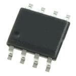
| 产品图片 |
|
| rohs | 符合RoHS无铅 / 符合限制有害物质指令(RoHS)规范要求 |
| 产品系列 | 放大器 IC,视频放大器,ON Semiconductor NE592D8G- |
| 数据手册 | |
| 产品型号 | NE592D8G |
| Pd-功率耗散 | 790 mW |
| 产品 | Video Amplifiers |
| 产品种类 | 视频放大器 |
| 供应商器件封装 | 8-SOIC N |
| 其它名称 | NE592D8G-ND |
| 包装 | 管件 |
| 压摆率 | - |
| 商标 | ON Semiconductor |
| 安装类型 | 表面贴装 |
| 安装风格 | SMD/SMT |
| 封装 | Tube |
| 封装/外壳 | 8-SOIC(0.154",3.90mm 宽) |
| 封装/箱体 | SOIC-8 Narrow |
| 工作电源电压 | +/- 8 V |
| 工厂包装数量 | 98 |
| 应用 | 通用 |
| 最大功率耗散 | 790 mW |
| 最大双重电源电压 | +/- 8 V |
| 最大工作温度 | + 70 C |
| 最小工作温度 | 0 C |
| 标准包装 | 98 |
| 电压-电源,单/双 (±) | ±3 V ~ 8 V |
| 电流-电源 | 18mA |
| 电流-输出/通道 | 10mA |
| 电源电流 | 24 mA |
| 电路数 | 1 |
| 系列 | NE592 |
| 输出类型 | 差分 |
| 通道数量 | 1 Channel |


- 商务部:美国ITC正式对集成电路等产品启动337调查
- 曝三星4nm工艺存在良率问题 高通将骁龙8 Gen1或转产台积电
- 太阳诱电将投资9.5亿元在常州建新厂生产MLCC 预计2023年完工
- 英特尔发布欧洲新工厂建设计划 深化IDM 2.0 战略
- 台积电先进制程称霸业界 有大客户加持明年业绩稳了
- 达到5530亿美元!SIA预计今年全球半导体销售额将创下新高
- 英特尔拟将自动驾驶子公司Mobileye上市 估值或超500亿美元
- 三星加码芯片和SET,合并消费电子和移动部门,撤换高东真等 CEO
- 三星电子宣布重大人事变动 还合并消费电子和移动部门
- 海关总署:前11个月进口集成电路产品价值2.52万亿元 增长14.8%


PDF Datasheet 数据手册内容提取
NE592 Video Amplifier The NE592 is a monolithic, two-stage, differential output, wideband video amplifier. It offers fixed gains of 100 and 400 without external components and adjustable gains from 400 to 0 with one external resistor. The input stage has been designed so that with the addition of a few external reactive elements between the gain select terminals, the circuit can function as a high-pass, low-pass, or wwwwww..oonnsseemmii..ccoomm band-pass filter. This feature makes the circuit ideal for use as a MARKING video or pulse amplifier in communications, magnetic memories, DIAGRAMS display, video recorder systems, and floppy disk head amplifiers. Now available in an 8-pin version with fixed gain of 400 without 8 external components and adjustable gain from 400 to 0 with one 1 SOIC−8 NE592 external resistor. D SUFFIX ALYW CASE 751 (cid:2) Features 1 • 120 MHz Unity Gain Bandwidth • Adjustable Gains from 0 to 400 • 14 Adjustable Pass Band • 1 SOIC−14 NE592D14G No Frequency Compensation Required D SUFFIX AWLYWW • CASE 751A Wave Shaping with Minimal External Components • 1 MIL-STD Processing Available • These Devices are Pb−Free and are RoHS Compliant A = Assembly Location L, WL = Wafer Lot Applications Y = Year • W, WW = Work Week Floppy Disk Head Amplifier (cid:2) or G = Pb−Free Package • Video Amplifier • Pulse Amplifier in Communications • Magnetic Memory ORDERING INFORMATION • Video Recorder Systems See detailed ordering and shipping information in the package dimensions section on page 8 of this data sheet. +V R1 R2 R8 R10 R9 Q6 Q5 Q4 Q3 R11 OUTPUT 1 INPUT 1 INPUT 2 Q1 Q2 R12 G1A G1B OUTPUT 2 R3 R5 G2A G2B Q7B Q8 Q9 Q10 Q7A Q11 R7A R7B R15 R16 R13 R14 ‐V Figure 1. Block Diagram © Semiconductor Components Industries, LLC, 2016 1 Publication Order Number: March, 2016 − Rev. 5 NE592/D
NE592 PIN CONNECTIONS SOIC-14 SOIC-8 INPUT 2 1 14 INPUT 1 INPUT 2 1 8 INPUT 1 NC 2 13 NC G1B GAIN SELECT 2 7 G1A GAIN SELECT V‐ 3 6 V+ G2B GAIN SELECT 3 12 G2A GAIN SELECT OUTPUT 2 4 5 OUTPUT 1 G1B GAIN SELECT 4 11 G1A GAIN SELECT (Top View) V‐ 5 10 V+ NC 6 9 NC OUTPUT 2 7 8 OUTPUT 1 (Top View) MAXIMUM RATINGS (TA = +25°C, unless otherwise noted.) Rating Symbol Value Unit Supply Voltage VCC (cid:2)8.0 V Differential Input Voltage VIN (cid:2)5.0 V Common-Mode Input Voltage VCM (cid:2)6.0 V Output Current IOUT 10 mA Operating Ambient Temperature Range TA 0 to +70 °C Operating Junction Temperature TJ 150 °C Storage Temperature Range TSTG 65 to +150 °C Maximum Power Dissipation, TA = 25°C (Still Air) (Note 1) PD MAX W SOIC-14 Package 0.98 SOIC-8 Package 0.79 Thermal Resistance, Junction−to−Ambient R(cid:2)JA °C/W SOIC-14 Package 145 SOIC-8 Package 182 Stresses exceeding those listed in the Maximum Ratings table may damage the device. If any of these limits are exceeded, device functionality should not be assumed, damage may occur and reliability may be affected. 1. Derate above 25°C at the following rates: SOIC-14 package at 6.9 mW/°C SOIC-8 package at 5.5 mW/°C www.onsemi.com 2
NE592 DC ELECTRICAL CHARACTERISTICS (VSS = (cid:2)6.0 V, VCM = 0, typicals at TA = +25°C, min and max at 0°C (cid:3) TA (cid:3) 70°C, unless otherwise noted. Recommended operating supply voltages VS = (cid:2)6.0 V.) Characteristic Test Conditions Symbol Min Typ Max Unit Differential Voltage Gain AVOL V/V Gain 1 (Note 2) RL = 2.0 k(cid:3), VOUT = 3.0 VP-P 250 400 600 Gain 2 (Notes 3 and 4) 80 100 120 Input Resistance RIN k(cid:3) Gain 1 (Note 2) − − 4.0 − Gain 2 (Notes 3 and 4) TA = 25°C 10 30 − 0°C (cid:3) TA (cid:3) 70°C 8.0 − − Input Capacitance Gain 2 (Note 4) CIN − 2.0 − pF Input Offset Current TA = 25°C IOS − 0.4 5.0 (cid:4)A 0°C (cid:3) TA (cid:3) 70°C − − 6.0 Input Bias Current TA = 25°C IBIAS − 9.0 30 (cid:4)A 0°C (cid:3) TA (cid:3) 70°C − − 40 Input Noise Voltage BW 1.0 kHz to 10 MHz VNOISE − 12 − (cid:4)VRMS Input Voltage Range − VIN (cid:2)1.0 − − V Common-Mode Rejection Ratio VCM (cid:2)1.0 V, f < 100 kHz, TA = 25°C CMRR 60 86 − dB Gain 2 (Note 4) VCM (cid:2)1.0 V, f < 100 kHz, 50 − − 0°C (cid:3) TA (cid:3) 70°C VCM (cid:2)1.0 V, f < 5.0 MHz − 60 − Supply Voltage Rejection Ratio (cid:5)VS = (cid:2)0.5 V PSRR 50 70 − dB Gain 2 (Note 4) Output Offset Voltage VOS V Gain 1 RL = (cid:4) − − 1.5 Gain 2 (Note 4) RL = (cid:4) − − 1.5 Gain 3 (Note 5) RL = (cid:4), TA = 25°C − 0.35 0.75 Gain 3 (Note 5) RL = (cid:4), 0°C (cid:3) TA (cid:3) 70°C − − 1.0 Output Common-Mode Voltage RL = (cid:4), TA = 25°C VCM 2.4 2.9 3.4 V Output Voltage Swing Differential RL = 2.0 k(cid:3), TA = 25°C VOUT 3.0 4.0 − V RL = 2.0 k(cid:3), 0°C (cid:3) TA (cid:3) 70°C 2.8 − − Output Resistance − ROUT − 20 − (cid:3) Power Supply Current RL = (cid:4), TA = 25°C ICC − 18 24 mA RL = (cid:4), 0°C (cid:3) TA (cid:3) 70°C − − 27 Product parametric performance is indicated in the Electrical Characteristics for the listed test conditions, unless otherwise noted. Product performance may not be indicated by the Electrical Characteristics if operated under different conditions. AC ELECTRICAL CHARACTERISTICS (TA = +25°C VSS = (cid:2)6.0 V, VCM = 0, unless otherwise noted. Recommended operating supply voltages VS = (cid:2)6.0 V.) Characteristic Test Conditions Symbol Min Typ Max Unit Bandwidth − BW MHz Gain 1 (Note 2) − 40 − Gain 2 (Notes 3 and 4) − 90 − Rise Time tR ns Gain 1 (Note 2) VOUT = 1.0 VP−P − 10.5 12 Gain 2 (Notes 3 and 4) − 4.5 − Propagation Delay tPD ns Gain 1 (Note 2) VOUT = 1.0 VP−P − 7.5 10 Gain 2 (Notes 3 and 4) − 6.0 − 2. Gain select Pins G1A and G1B connected together. 3. Gain select Pins G2A and G2B connected together. 4. Applies to 14-pin version only. 5. All gain select pins open. www.onsemi.com 3
NE592 TYPICAL PERFORMANCE CHARACTERISTICS dB 100 7.0 1.6 ON RATIO − 987000 GVTASA I==N 2 +256oVC NG − Vpp 65..00 VTRASL === 21+5k6o(cid:3)VC 111...420 VTRASL === 21+5k6oVC EJECTI 6500 GE SWI 4.0 00..86 GAIN 2 DE R 40 OLTA 3.0 0.4 GAIN 1 MO 30 T V 2.0 0.2 MMON- 2100 OUTPU 1.0 -0.02 O C 0 0 -0.4 10k 100k 1M 10M 100M 1 5 10 50100 5001000 -15-10 -5 0 5 10 15 20 25 30 35 FREQUENCY − Hz FREQUENCY − MHz TIME − ns Figure 2. Common−Mode Figure 3. Output Voltage Swing Figure 4. Pulse Response Rejection Ratio as a Function as a Function of Frequency of Frequency 28 1.6 1.6 TA = 25oC 1.4 GTAA I=N 2 25oC 1.4 GVSA I=N +26V URRENT − mA 2240 OLTAGE − V 1100....2086 RL = 1k(cid:3) VVVSSS === +++836VVV OLTAGE − V 1100....2086 TRaLm =b 1=k 0(cid:3)oC TA = 25oC C V V PLY 16 PUT 0.4 PUT 0.4 TA = 70oC UP UT 0.2 UT 0.2 S 12 O 0 O 0 -0.2 -0.2 8 -0.4 -0.4 3 4 5 6 7 8 -15 -10 -5 0 5 10 15 20 25 30 35 -15-10 -5 0 5 10 15 20 25 30 35 SUPPLY VOLTAGE − +V TIME − ns TIME − ns Figure 5. Supply Current as Figure 6. Pulse Response as Figure 7. Pulse Response as a Function of Temperature a Function of Supply Voltage a Function of Temperature 1.4 1.10 60 RELATIVE VOLTAGE GAIN 11111000........0000099986420864 GAIN 1 VGSA I=N + 26V GLE ENDED VOLTAGE GAIN − dB 54321000000 TATT AA= ==− 521552oo5CCoC GVRSLA I==N 1+2k6(cid:3)V RELATIVE VOLTAGE GAIN 11110000........32109876 GAIN 2 GAIN 1 Tamb = 25oC 0.92 N 0.5 SI 0.90 -10 0.4 0 10 20 30 40 50 60 70 1 5 10 50100 5001000 3 4 5 6 7 8 TEMPERATURE − oC FREQUENCY − MHz SUPPLY VOLTAGE − +V Figure 8. Voltage Gain as a Figure 9. Gain vs. Frequency Figure 10. Voltage Gain as a Function of Temperature as a Function of Temperature Function of Supply Voltage www.onsemi.com 4
NE592 TYPICAL PERFORMANCE CHARACTERISTICS 60 1000 OLTAGE GAIN − dB 543000 GTRALA I==N 2 125ko(cid:3)C 114 135291241 78 00..22(cid:4)(cid:4)FF LTAGE GAIN − V/V 11000 TF V A ISfG ==U= 1R2+05E60oV k2CHz ED V 20 VS = +8V L VO 1 D A LE EN 10 VS = +6V 51(cid:2) 51(cid:2) RADJ 1k(cid:2) 1k(cid:2) RENTI .1 G E SIN -100 VS = +3V VS = +6V TA = 25oC DIFF .01 1 5 10 50 100 5001000 1 10 100 1K 10K 100K 1M FREQUENCY − MHz RADJ − (cid:3) Figure 11. Gain vs. Frequency Figure 12. Voltage Gain Adjust Figure 13. Voltage Gain as a as a Function of Supply Voltage Circuit Function of RADJ (Figure 2) 21 70 7.0 SUPPLY CURRENT − mA 211111098765 VS = +6V OVERDRIVE RECOVERY TIME − ns 654321000000 VTGASA I==N 2 +256oVC OUTPUT VOLTAGE SWING − V OROUTPUT SINK CURRENT − mA 654321......000000 VOLTAGE CUTAR R=E 2N5ToC 14 0 0 -60 -20 20 60 100 140 0 20 40 60 80 100120140160180200 3.0 4.0 5.0 6.0 7.0 8.0 TEMPERATURE − oC DIFFERENTIAL INPUT VOLTAGE − mV SUPPLY VOLTAGE − +V Figure 14. Supply Current as a Figure 15. Differential Overdrive Figure 16. Output Voltage and Function of Temperature Recovery Time Current Swing as a Function of Supply Voltage 7.0 70 100 Vpp 6.0 VTAS == 2+56oVC Ω 60 GVSA I=N +26V ms 90 GVSA I=N +26V WING − 5.0 NCE − K 50 μGE − Vr 8700 TBAW = = 2 150oMCHz TPUT VOLTAGE S 432...000 INPUT RESISTA 432000 UT NOISE VOLTA 6543200000 OU 1.0 10 INP 10 0 0 0 10 50 100 5001K 5K10K -60 -20 0 20 60 100 140 1 10 100 1K 10K LOAD RESISTANCE − (cid:3) TEMPERATURE − oC SOURCE RESISTANCE − (cid:3) Figure 17. Output Voltage Figure 18. Input Resistance as a Figure 19. Input Noise Voltage Swing as a Function of Load Function of Temperature as a Function of Source Resistance Resistance www.onsemi.com 5
NE592 TYPICAL PERFORMANCE CHARACTERISTICS 0 0 GAIN 2 VS = +6V ES -5 VTAS == 2+56oVC ES -50 TA = 25oC RE RE -100 G G SHIFT − DE --1105 SHIFT − DE --125000 GAIN 1 GAIN 2 SE SE -250 A A PH -20 PH -300 -350 -25 1 10 100 1000 0 1 2 3 4 5 6 7 8 9 10 FREQUENCY − MHz FREQUENCY − MHz Figure 20. Phase Shift as a Figure 21. Phase Shift as a Function of Frequency Function of Frequency 60 VS = +6V 50 GAIN 1 TRaLm =b 1 =K (cid:3)25oC 4300 VTGASA I==N 2 +356oVC AIN − dB 4300 GAIN 2 AIN − dB 2100 OLTAGE G 2100 OLTAGE G --12000 V V -30 0 -40 -50 1 10 100 1000 .01 .1 1 10 100 1000 FREQUENCY − MHz FREQUENCY − MHz Figure 22. Voltage Gain as a Figure 23. Voltage Gain as a Function of Frequency Function of Frequency TEST CIRCUITS (TA = 25°C, unless otherwise noted.) VIN 592 RL VOUT 51(cid:3) 51(cid:3) 0.2(cid:4)F ein 592 0.2(cid:4)F eout eout 51(cid:3) 51(cid:3) 1k(cid:2) 1k(cid:2) Figure 24. Test Circuits www.onsemi.com 6
NE592 +6 2re 11 14 10 V1 592 V0 NOTE: 1 7 V0(s) 1.4(cid:7)104 5 v1(s) (cid:6)Z(S) (cid:8) 2re 4 1.4 (cid:7) 104 Z (cid:6) Z(S) (cid:8) 32 -6 +6 Basic Configuration 0.2(cid:4)F +5 +6 11 14 10 9 4 8 10 8 2K(cid:3) 1 529 7 V1 592 V0 14 11 Q 1 7 0.2(cid:4)F 10 8 5 592 4 7 1 4 5 2 5 C 2K(cid:3) Q -6 AMPLITUDE: 1‐10 mV p‐p 3 NOTE: FREQUENCY: 1‐4 MHz 6 ‐6 For frequency F1 << 1/2 π (32) C V (cid:5)1.4x10⁴C dVi O dT READ HEAD DIFFERENTIATOR/AMPLIFIER ZERO CROSSING DETECTOR Differentiation with High Disc/Tape Phase-Modulated Readback Systems Common-Mode Noise Rejection Figure 25. Typical Applications Z NETWORK FILTER V0 (s) TRANSFER TYPE V1 (s) FUNCTION (cid:10) (cid:12) R L 1.4(cid:9)104 1 LOW PASS L s(cid:8)R(cid:11)L (cid:10) (cid:12) R C 1.4(cid:9)104 s HIGH PASS R s(cid:8)1(cid:11)RC (cid:10) (cid:12) R L C 1.4(cid:9)104 s BAND PASS L s2(cid:8)R(cid:11)Ls(cid:8)1(cid:11)LC L (cid:10) (cid:12) R 1.4(cid:9)104 s2(cid:8)1(cid:11)LC BAND REJECT R s2(cid:8)1(cid:11)LC(cid:8)s(cid:11)RC C NOTES: In the networks above, the R value used is assumed to include 2re, or approximately 32(cid:3). S = j(cid:3) (cid:3) = 2πf Figure 26. Filter Networks www.onsemi.com 7
NE592 ORDERING INFORMATION Device Temperature Range Package Shipping† NE592D8G 98 Units/Rail SOIC−8 NE592D8R2G (Pb−Free) 2500 / Tape & Reel 0 to +70°C NE592D14G 55 Units/Rail SOIC−14 NE592D14R2G (Pb−Free) 2500 / Tape & Reel †For information on tape and reel specifications, including part orientation and tape sizes, please refer to our Tape and Reel Packaging Specification Brochure, BRD8011/D. www.onsemi.com 8
NE592 PACKAGE DIMENSIONS SOIC−8 NB CASE 751−07 ISSUE AK NOTES: −X− 1. DIMENSIONING AND TOLERANCING PER ANSI Y14.5M, 1982. A 2. CONTROLLING DIMENSION: MILLIMETER. 3. DIMENSION A AND B DO NOT INCLUDE MOLD PROTRUSION. 4. MAXIMUM MOLD PROTRUSION 0.15 (0.006) 8 5 PER SIDE. 5. DIMENSION D DOES NOT INCLUDE DAMBAR B S 0.25 (0.010) M Y M PROTRUSION. ALLOWABLE DAMBAR PROTRUSION SHALL BE 0.127 (0.005) TOTAL 1 IN EXCESS OF THE D DIMENSION AT −Y− 4 K 6. M75A1X−I0M1U TMH RMUA T7E51R−IA06L CAROEN DOIBTSIOONL.ETE. NEW STANDARD IS 751−07. G MILLIMETERS INCHES DIM MIN MAX MIN MAX A 4.80 5.00 0.189 0.197 C NX 45(cid:3) B 3.80 4.00 0.150 0.157 SEATING C 1.35 1.75 0.053 0.069 PLANE D 0.33 0.51 0.013 0.020 −Z− G 1.27 BSC 0.050 BSC H 0.10 0.25 0.004 0.010 0.10 (0.004) J 0.19 0.25 0.007 0.010 H D M J K 0.40 1.27 0.016 0.050 M 0 (cid:3) 8 (cid:3) 0 (cid:3) 8 (cid:3) N 0.25 0.50 0.010 0.020 0.25 (0.010)M Z Y S X S S 5.80 6.20 0.228 0.244 SOLDERING FOOTPRINT* 1.52 0.060 7.0 4.0 0.275 0.155 0.6 1.270 0.024 0.050 (cid:13) (cid:14) mm SCALE 6:1 inches *For additional information on our Pb−Free strategy and soldering details, please download the ON Semiconductor Soldering and Mounting Techniques Reference Manual, SOLDERRM/D. www.onsemi.com 9
NE592 PACKAGE DIMENSIONS SOIC−14 CASE 751A−03 ISSUE L D A NOTES: B 1.DIMENSIONING AND TOLERANCING PER ASME Y14.5M, 1994. 2.CONTROLLING DIMENSION: MILLIMETERS. 14 8 3.DIMENSION b DOES NOT INCLUDE DAMBAR A3 PROTRUSION. ALLOWABLE PROTRUSION SHALL BE 0.13 TOTAL IN EXCESS OF AT MAXIMUM MATERIAL CONDITION. H E 4.DIMENSIONS D AND E DO NOT INCLUDE MOLD PROTRUSIONS. L 5.MAXIMUM MOLD PROTRUSION 0.15 PER SIDE. 1 7 DETAIL A MILLIMETERS INCHES 0.25 M B M 13Xb DIM MIN MAX MIN MAX A 1.35 1.75 0.054 0.068 0.25 M C A S B S A1 0.10 0.25 0.004 0.010 A3 0.19 0.25 0.008 0.010 h DETAIL A b 0.35 0.49 0.014 0.019 A D 8.55 8.75 0.337 0.344 X 45(cid:3) E 3.80 4.00 0.150 0.157 e 1.27 BSC 0.050 BSC H 5.80 6.20 0.228 0.244 h 0.25 0.50 0.010 0.019 0.10 e A1 C SEATING M ML 0.400 (cid:3) 1.275 (cid:3) 0.0106 (cid:3) 0.0479 (cid:3) PLANE SOLDERING FOOTPRINT* 6.50 14X 1.18 1 1.27 PITCH 14X 0.58 DIMENSIONS: MILLIMETERS *For additional information on our Pb−Free strategy and soldering details, please download the ON Semiconductor Soldering and Mounting Techniques Reference Manual, SOLDERRM/D. ON Semiconductor and the are registered trademarks of Semiconductor Components Industries, LLC (SCILLC) or its subsidiaries in the United States and/or other countries. SCILLC owns the rights to a number of patents, trademarks, copyrights, trade secrets, and other intellectual property. A listing of SCILLC’s product/patent coverage may be accessed at www.onsemi.com/site/pdf/Patent−Marking.pdf. SCILLC reserves the right to make changes without further notice to any products herein. SCILLC makes no warranty, representation or guarantee regarding the suitability of its products for any particular purpose, nor does SCILLC assume any liability arising out of the application or use of any product or circuit, and specifically disclaims any and all liability, including without limitation special, consequential or incidental damages. “Typical” parameters which may be provided in SCILLC data sheets and/or specifications can and do vary in different applications and actual performance may vary over time. All operating parameters, including “Typicals” must be validated for each customer application by customer’s technical experts. SCILLC does not convey any license under its patent rights nor the rights of others. SCILLC products are not designed, intended, or authorized for use as components in systems intended for surgical implant into the body, or other applications intended to support or sustain life, or for any other application in which the failure of the SCILLC product could create a situation where personal injury or death may occur. Should Buyer purchase or use SCILLC products for any such unintended or unauthorized application, Buyer shall indemnify and hold SCILLC and its officers, employees, subsidiaries, affiliates, and distributors harmless against all claims, costs, damages, and expenses, and reasonable attorney fees arising out of, directly or indirectly, any claim of personal injury or death associated with such unintended or unauthorized use, even if such claim alleges that SCILLC was negligent regarding the design or manufacture of the part. SCILLC is an Equal Opportunity/Affirmative Action Employer. This literature is subject to all applicable copyright laws and is not for resale in any manner. PUBLICATION ORDERING INFORMATION LITERATURE FULFILLMENT: N. American Technical Support: 800−282−9855 Toll Free ON Semiconductor Website: www.onsemi.com Literature Distribution Center for ON Semiconductor USA/Canada 19521 E. 32nd Pkwy, Aurora, Colorado 80011 USA Europe, Middle East and Africa Technical Support: Order Literature: http://www.onsemi.com/orderlit Phone: 303−675−2175 or 800−344−3860 Toll Free USA/Canada Phone: 421 33 790 2910 Fax: 303−675−2176 or 800−344−3867 Toll Free USA/Canada Japan Customer Focus Center For additional information, please contact your local Email: orderlit@onsemi.com Phone: 81−3−5817−1050 Sales Representative www.onsemi.com NE592/D 10
Mouser Electronics Authorized Distributor Click to View Pricing, Inventory, Delivery & Lifecycle Information: O N Semiconductor: NE592D14G NE592D14R2G NE592D8G NE592D8R2G