ICGOO在线商城 > 集成电路(IC) > 线性 - 放大器 - 视频放大器和频缓冲器 > AD830JR
 Datasheet下载
- 型号: AD830JR
- 制造商: Analog
- 库位|库存: xxxx|xxxx
- 要求:
| 数量阶梯 | 香港交货 | 国内含税 |
| +xxxx | $xxxx | ¥xxxx |
查看当月历史价格
查看今年历史价格
AD830JR产品简介:
ICGOO电子元器件商城为您提供AD830JR由Analog设计生产,在icgoo商城现货销售,并且可以通过原厂、代理商等渠道进行代购。 AD830JR价格参考¥57.53-¥64.73。AnalogAD830JR封装/规格:线性 - 放大器 - 视频放大器和频缓冲器, Video Amp, 1 Differential 8-SOIC。您可以下载AD830JR参考资料、Datasheet数据手册功能说明书,资料中有AD830JR 详细功能的应用电路图电压和使用方法及教程。
AD830JR是由Analog Devices Inc.生产的一款线性放大器,属于视频放大器和频率缓冲器类别。它具有高带宽、低失真和低噪声的特点,适用于多种高性能模拟信号处理场景。以下是AD830JR的主要应用场景:

1. 视频信号处理:
   AD830JR广泛用于视频信号的放大和缓冲,支持高质量的视频传输。它能够处理复合视频信号、S-Video以及分量视频信号,适用于电视、监视器、摄像头和其他视频设备。

2. 宽带通信系统:
   由于其高带宽特性(超过150MHz),AD830JR适合用在宽带通信系统中,例如有线电视(CATV)前端、射频(RF)信号调理和数据传输链路中的信号增强。

3. 医疗成像设备:
   在超声波成像、X射线扫描和其他医疗成像应用中,AD830JR可以用来放大和处理高频模拟信号,确保图像清晰度和准确性。

4. 测试与测量仪器:
   该器件常用于示波器、信号发生器和频谱分析仪等测试设备中,以提供精确的信号放大和缓冲功能,保证测量结果的可靠性。

5. 音频处理:
   尽管主要定位为视频放大器,AD830JR也可以用于高端音频设备中,如专业音响系统和录音设备,提供低失真的信号放大。

6. 工业自动化与控制:
   在工业领域,AD830JR可用于传感器信号调理、数据采集系统和过程控制系统,帮助提高信号质量和系统响应速度。

总之,AD830JR凭借其优异的性能参数,成为需要高速、高精度信号处理的各种应用的理想选择。
| 参数 | 数值 |
| -3db带宽 | 85MHz |
| 产品目录 | 集成电路 (IC)半导体 |
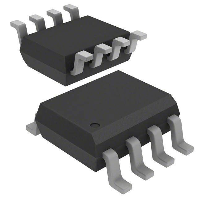
| 描述 | IC VIDEO DIFF AMP HS 8-SOIC差分放大器 HI SPEED VIDEO |
| 产品分类 | |
| 品牌 | Analog Devices |
| 产品手册 | |
| 产品图片 |
|
| rohs | 否不符合限制有害物质指令(RoHS)规范要求 |
| 产品系列 | 放大器 IC,差分放大器,Analog Devices AD830JR- |
| 数据手册 | |
| 产品型号 | AD830JR |
| PCN过时产品 | |
| 产品种类 | 差分放大器 |
| 供应商器件封装 | 8-SOIC |
| 包装 | 管件 |
| 压摆率 | 360 V/µs |
| 商标 | Analog Devices |
| 增益带宽生成 | 85 MHz |
| 安装类型 | 表面贴装 |
| 安装风格 | SMD/SMT |
| 封装 | Tube |
| 封装/外壳 | 8-SOIC(0.154",3.90mm 宽) |
| 封装/箱体 | SOIC-8 |
| 工厂包装数量 | 98 |
| 应用 | 差分 |
| 最大双重电源电压 | +/- 16.5 V |
| 最大工作温度 | + 70 C |
| 最小工作温度 | 0 C |
| 标准包装 | 98 |
| 电压-电源,单/双 (±) | 8 V ~ 33 V, ±4 V ~ 16.5 V |
| 电流-电源 | 14.5mA |
| 电流-输出/通道 | 50mA |
| 电路数 | 1 |
| 系列 | AD830 |
| 输出类型 | - |


- 商务部:美国ITC正式对集成电路等产品启动337调查
- 曝三星4nm工艺存在良率问题 高通将骁龙8 Gen1或转产台积电
- 太阳诱电将投资9.5亿元在常州建新厂生产MLCC 预计2023年完工
- 英特尔发布欧洲新工厂建设计划 深化IDM 2.0 战略
- 台积电先进制程称霸业界 有大客户加持明年业绩稳了
- 达到5530亿美元!SIA预计今年全球半导体销售额将创下新高
- 英特尔拟将自动驾驶子公司Mobileye上市 估值或超500亿美元
- 三星加码芯片和SET,合并消费电子和移动部门,撤换高东真等 CEO
- 三星电子宣布重大人事变动 还合并消费电子和移动部门
- 海关总署:前11个月进口集成电路产品价值2.52万亿元 增长14.8%


PDF Datasheet 数据手册内容提取
High Speed, Video Difference Amplifier Data Sheet AD830 FEATURES CONNECTION DIAGRAM Differential amplification Wide common-mode voltage range: +12.8 V to −12 V X1 1 GM AD830 8 VP Differential voltage: ±2 V X2 2 7 OUT A = 1 High CMRR: 60 dB at 4 MHz Y1 3 6 NC BF8a5us iMtlt d-Hiynzn duainmfifteiycr epgneatriinfao lbr camlnipadnpwcineidg t lhe vel: ±2.3 V Y2 4 NC =G MNO CONNCECT 5 VN 00881-001 35 ns settling time to 0.1% Figure 1. 8-Lead Plastic PDIP (N), CERDIP (Q), and SOIC (RN) Packages 360 V/μs slew rate 110 Symmetrical dynamic response 100 Excellent video specifications Differential gain error: 0.06% 90 Differential phase error: 0.08° 80 15 MHz (0.1 dB) bandwidth B) VS= ±15V d Flexible operation R ( 70 R High output drive of ±50 mA min M C 60 Specified with both ±5 V and ±15 V supplies VS= ±5V Low distortion: THD = −72 dB @ 4 MHz 50 Excellent DC performance: 3 mV max input 40 Offset voltage 30 ADiPffPerLeInCtiAalT liInOeN reSc eiver 1k 10k FREQU1E0N0kCY (Hz) 1M 10M 00881-002 Figure 2. Common-Mode Rejection Ratio vs. Frequency High speed level shifter High speed in-amp Differential to single-ended conversion Good gain flatness and excellent differential gain of 0.06% and Resistorless summation and subtraction phase of 0.08° make the AD830 suitable for many video system High speed analog-to-digital converter applications. Furthermore, the AD830 is suited for general-purpose signal processing from dc to 10 MHz. GENERAL DESCRIPTION 9 VS = ±5V The AD830 is a wideband, differencing amplifier designed for use 6 RL = 150Ω at video frequencies but also useful in many other applications. It 3 accurately amplifies a fully differential signal at the input and CL = 33pF 0 produces an output voltage referred to a user-chosen level. The –3 undesired common-mode signal is rejected, even at high dB) CL = 4.7pF frequencies. High impedance inputs ease interfacing to finite N ( –6 AI source impedances and, thus, preserve the excellent common- G –9 mode rejection. In many respects, it offers significant –12 improvements over discrete difference amplifier approaches, in CL = 15pF –15 particular in high frequency common-mode rejection. –18 The wide common-mode and differential voltage range of the –21 AapDp8li3ca0t imonaks eb uitt p aat rltoicwuelra rploy wueser fduils asinpda tfiloenxi tbhlea nin d liesvcerle tseh isfotiluntgi ons. 10k 100k F1RMEQUENCY 1(0HMz) 100M 1G 00881-003 Figure 3. Closed-Loop Gain vs. Frequency, Gain = +1 Low distortion is preserved over the many possible differential and common-mode voltages at the input and output. Rev. D Document Feedback Information furnished by Analog Devices is believed to be accurate and reliable. However, no responsibility is assumed by Analog Devices for its use, nor for any infringements of patents or other One Technology Way, P.O. Box 9106, Norwood, MA 02062-9106, U.S.A. rights of third parties that may result from its use. Specifications subject to change without notice. No license is granted by implication or otherwise under any patent or patent rights of Analog Devices. Tel: 781.329.4700 ©2005–2018 Analog Devices, Inc. All rights reserved. Trademarks and registered trademarks are the property of their respective owners. Technical Support www.analog.com
AD830 Data Sheet TABLE OF CONTENTS Features .............................................................................................. 1 Theory of Operation ...................................................................... 11 Applications ....................................................................................... 1 Traditional Differential Amplification .................................... 11 Connection Diagram ....................................................................... 1 Problems With the Op Amp Based Approach ....................... 11 General Description ......................................................................... 1 AD830 for Differential Amplification ..................................... 11 Revision History ............................................................................... 2 Advantageous Properties of the AD830 .................................. 11 Specifications ..................................................................................... 3 Understanding the AD830 Topology ...................................... 11 Absolute Maximum Ratings ............................................................ 7 Interfacing the Input .................................................................. 12 Maximum Power Dissipation ..................................................... 7 Supplies, Bypassing, and Grounding (Figure 34) ................... 14 Thermal Resistance ...................................................................... 7 AC-Coupled Line Receiver ....................................................... 17 ESD Caution .................................................................................. 7 Outline Dimensions ....................................................................... 19 Typical Performance Characteristics ............................................. 8 Ordering Guide .......................................................................... 20 REVISION HISTORY 1/2018—Rev. C to Rev. D Change to Table 4 ............................................................................. 7 Changes to Ordering Guide .......................................................... 20 3/2010—Rev. B to Rev. C Updated Format .................................................................. Universal Changes to Ordering Guide .......................................................... 20 1/2003—Rev. A to Rev. B. Updated Ordering Guide ................................................................ 4 Change to Figure 30 ...................................................................... 14 Updated Outline Dimensions ..................................................... 15 Rev. D | Page 2 of 20
Data Sheet AD830 SPECIFICATIONS V = ±15 V, R = 150 Ω, C = 5 pF, T = 25°C, unless otherwise noted. S LOAD LOAD A Table 1. AD830J/AD830A AD830S1 Parameter Conditions Min Typ Max Min Typ Max Unit DYNAMIC CHARACTERISTICS 3 dB Small Signal Bandwidth Gain = +1, V = 100 mV rms 75 85 75 85 MHz OUT 0.1 dB Gain Flatness Gain = +1, V = 100 mV rms 11 15 11 15 MHz OUT Frequency Differential Gain Error 0 V to 0.7 V, frequency = 0.06 0.09 0.06 0.09 % 4.5 MHz Differential Phase Error 0 V to 0.7 V, frequency = 0.08 0.12 0.08 0.12 Degrees 4.5 MHz Slew Rate 2 V step, R = 500 Ω 360 360 V/μs L 4 V step, R = 500 Ω 350 350 V/μs L 3 dB Large Signal Bandwidth Gain = +1, V = 1 V rms 38 45 38 45 MHz OUT Settling Time, Gain = +1 V = 2 V step, to 0.1% 25 25 ns OUT V = 4 V step, to 0.1% 35 35 ns OUT Harmonic Distortion 2 V p-p, frequency = 1 MHz −82 −82 dBc 2 V p-p, frequency = 4 MHz −72 −72 dBc Input Voltage Noise frequency = 10 kHz 27 27 nV/√Hz Input Current Noise 1.4 1.4 pA/√Hz DC PERFORMANCE Offset Voltage Gain = +1 ±1.5 ±3 ±1.5 ±3 mV Gain = +1, T − T ±5 ±7 mV MIN MAX Open-Loop Gain DC 64 69 64 69 dB Gain Error R = 1 kΩ, G = ±1 ±0.1 ±0.6 ±0.1 ±0.6 % L Peak Nonlinearity, R = 1 kΩ, −1 V ≤ X ≤ +1 V 0.01 0.03 0.01 0.03 % FS L Gain = +1 −1.5 V ≤ X ≤ +1.5 V 0.035 0.07 0.035 0.07 % FS −2 V ≤ X ≤ +2 V 0.15 0.4 0.15 0.4 % FS Input Bias Current V = 0 V, 25°C to T 5 10 5 10 μA IN MAX V = 0 V, T 7 13 8 17 μA IN MIN Input Offset Current V = 0 V, T − T 0.1 1 0.1 1 μA IN MIN MAX INPUT CHARACTERISTICS Differential Voltage Range V = 0 ±2.0 ±2.0 V CM Differential Clipping Level2 Pin 1 and Pin 2 inputs only ±2.1 ±2.3 ±2.1 ±2.3 V Common-Mode Voltage V = ±1 V −12.0 +12.8 −12.0 +12.8 V DM Range CMRR DC, Pin 1/Pin 2, ±10 V 90 100 90 100 dB DC, Pin 1/Pin 2, ±10 V, T − T 88 86 dB MIN MAX Frequency = 4 MHz 55 60 55 60 dB Input Resistance 370 370 kΩ Input Capacitance 2 2 pF OUTPUT CHARACTERISTICS Output Voltage Swing R ≥ 1 kΩ ±12 +13.8/−13.8 ±12 +13.8/−13.8 V L R ≥ 1 kΩ, ±16.5 V ±13 +15.3/−14.7 ±13 +15.3/−14.7 V L S Short-Circuit Current Short to ground ±80 ±80 mA Output Current R = 150 Ω ±50 ±50 mA L Rev. D | Page 3 of 20
AD830 Data Sheet AD830J/AD830A AD830S1 Parameter Conditions Min Typ Max Min Typ Max Unit POWER SUPPLIES Operating Range ±4 ±16.5 ± 4 ±16.5 V Quiescent Current T – T 14.5 17 14.5 17 mA MIN MAX +PSRR (to V) DC, G = +1 86 86 dB P −PSRR (to V ) DC, G = +1 68 68 dB N PSRR DC, G = +1, ±5 to ±15 V 66 71 66 71 dB S PSRR DC, G = +1, ±5 to ±15 V S T − T 62 68 60 68 dB MIN MAX 1 See the Standard Military Drawing 5962-9313001MPA for specifications. 2 Clipping level function on X channel only. Rev. D | Page 4 of 20
Data Sheet AD830 V = ±5 V, R = 150 Ω, C = 5 pF, T = +25°C, unless otherwise noted. S LOAD LOAD A Table 2. AD830J/AD830A AD830S1 Parameter Conditions Min Typ Max Min Typ Max Units DYNAMIC CHARACTERISTICS 3 dB Small Signal Bandwidth Gain = +1, V = 100 mV rms 35 40 35 40 MHz OUT 0.1 dB Gain Flatness Frequency Gain = +1, V = 100 mV rms 5 6.5 5 6.5 MHz OUT Differential Gain Error 0 V to 0.7 V, frequency = 4.5 MHz, Gain = +2 0.14 0.18 0.14 0.18 % Differential Phase Error 0 V to 0.7 V, frequency = 4.5 MHz, Gain = +2 0.32 0.4 0.32 0.4 Degrees Slew Rate, Gain = +1 2 V step, R = 500 Ω 210 210 V/μs L 4 V step, R = 500 Ω 240 240 V/μs L 3 dB Large Signal Bandwidth Gain = +1, V = 1 V rms 30 36 30 36 MHz OUT Settling Time V = 2 V step, to 0.1% 35 35 ns OUT V = 4 V step, to 0.1% 48 48 ns OUT Harmonic Distortion 2 V p-p, frequency = 1 MHz −69 −69 dBc 2 V p-p, frequency = 4 MHz −56 −56 dBc Input Voltage Noise Frequency = 10 kHz 27 27 nV/√Hz Input Current Noise 1.4 1.4 pA/√Hz DC PERFORMANCE Offset Voltage Gain = +1 ±1.5 ±3 ±1.5 ±3 mV Gain = +1, T − T ±4 ±5 mV MIN MAX Open-Loop Gain DC 60 65 60 65 dB Unity Gain Accuracy R = 1 kΩ ±0.1 ±0.6 ±0.1 ±0.6 % L Peak Nonlinearity, R= 1 kΩ −1 V ≤ X ≤ +1 V 0.01 0.03 0.01 0.03 % FS L −1.5 V ≤ X ≤ +1.5 V 0.045 0.07 0.045 0.07 % FS −2 V ≤ X ≤ +2 V 0.23 0.4 0.23 0.4 % FS Input Bias Current V = 0 V, 25°C to T 5 10 5 10 μA IN MAX V = 0 V, T 7 13 8 17 μA IN MIN Input Offset Current V = 0 V, T − T 0.1 1 0.1 1 μA IN MIN MAX INPUT CHARACTERISTICS Differential Voltage Range V = 0 ±2.0 ±2.0 V CM Differential Clipping Level2 Pin 1 and Pin 2 inputs only ±2.0 ±2.2 ±2.0 ±2.2 V Common-Mode Voltage Range V = ±1 V −2.0 +2.9 −2.0 +2.9 V DM CMRR DC, Pin 1/Pin 2, +4 V to −2 V 90 100 90 100 dB DC, Pin 1/Pin 2, +4 V to −2 V, T − T 88 86 dB MIN MAX Frequency = 4 MHz 55 60 55 60 dB Input Resistance 370 370 kΩ Input Capacitance 2 2 pF OUTPUT CHARACTERISTICS Output Voltage Swing R ≥ 150 Ω ±3.2 ±3.5 ±3.2 ±3.5 V L R ≥ 150 Ω, ±4 V ±2.2 −2.4/+2.7 ±2.2 −2.4/+2.7 V L S Short-Circuit Current Short to ground −55/+70 −55/+70 mA Output Current ±40 ±40 mA Rev. D | Page 5 of 20
AD830 Data Sheet AD830J/AD830A AD830S1 Parameter Conditions Min Typ Max Min Typ Max Units POWER SUPPLIES Operating Range ±4 ±16.5 ±4 ±16.5 V Quiescent Current T − T 13.5 16 13.5 16 mA MIN MAX +PSRR (to V) DC, G = +1, offset 86 86 dB P −PSRR (to V ) DC, G = +1, Offset 68 68 dB N PSRR (Dual Supply) DC, G = +1, ±5 to ±15 V 66 71 66 71 dB S PSRR (Dual Supply) DC, G = +1, ±5 to ±15 V S T − T 62 68 60 68 dB MIN MAX 1 See Standard Military Drawing 5962-9313001MPA for specifications. 2 Clipping level function on X channel only. Rev. D | Page 6 of 20
Data Sheet AD830 ABSOLUTE MAXIMUM RATINGS MAXIMUM POWER DISSIPATION The maximum power that can be safely dissipated by the Table 3. AD830 is limited by the associated rise in junction temperature. Parameter Rating For the plastic packages, the maximum safe junction Supply Voltage ±18 V temperature is 145°C. For the CERDIP, the maximum junction Internal Power Dissipation Observe derating temperature is 175°C. If these maximums are exceeded curves momentarily, proper circuit operation will be restored as soon Output Short-Circuit Duration Observe derating as the die temperature is reduced. Leaving the AD830 in the curves overheated condition for an extended period can result in Common-Mode Input Voltage ±VS permanent damage to the device. To ensure proper operation, it Differential Input Voltage ±VS is important to observe the recommended derating curves. Storage Temperature Range (Q) −65°C to +150°C While the AD830 output is internally short-circuit protected, Storage Temperature Range (N) −65°C to +125°C this may not be sufficient to guarantee that the maximum Storage Temperature Range (RN) −65°C to +125°C junction temperature is not exceeded under all conditions. If Operating Temperature Range the output is shorted to a supply rail for an extended period, AD830J 0°C to +70°C then the amplifier may be permanently destroyed. AD830A −40°C to +85°C AD830S −55°C to +125°C THERMAL RESISTANCE Lead Temperature Range (Soldering 60 sec) 300°C θ is specified for the worst-case conditions, that is, a device JA Stresses at or above those listed under Absolute Maximum soldered in a circuit board for surface-mount packages. Ratings may cause permanent damage to the product. This is a Table 4. Thermal Resistance stress rating only; functional operation of the product at these Package Type θ Unit or any other conditions above those indicated in the operational JA 28-Lead PDIP Package 90 °C/W section of this specification is not implied. Operation beyond 8-Lead SOIC Package 155 °C/W the maximum operating conditions for extended periods may 8-Lead CERDIP Package 110 °C/W affect product reliability. ESD CAUTION 2.5 2.8 TJ MAX = 145°C 2.6 TJ MAX = 175°C 2.4 W)2.0 W) N ( N ( 2.2 TIO TIO 2.0 A A SIP1.5 SIP 1.8 S 8-LEAD PDIP S 1.6 DI DI R R 1.4 E E OW1.0 OW 1.2 8-LEAD CERDIP P P L L 1.0 A A OT0.5 OT 0.8 T T 8-LEAD SOIC 0.6 0.4 0–50 –30 –A1M0BIENT1 T0EMPER3A0TURE (5°C0) 70 90 00881-004 0.2–60 –40 –20 AM0BIEN2T0 TEM4P0ERAT6U0RE (8°C0) 100 120 140 00881-005 Figure 4. Maximum Power Dissipation vs. Temperature, PDIP and SOIC Packages Figure 5. Maximum Power Dissipation vs. Temperature, CERDIP Package Rev. D | Page 7 of 20
AD830 Data Sheet TYPICAL PERFORMANCE CHARACTERISTICS 110 100 100 90 TOVP @ ±±15V TOVP @ ±±5V 90 80 TO VN @ ±±15V 80 70 dB) VS= ±15V B)60 RR ( 70 R (d TO VN @ ±5V M R50 C 60 PS VS =± ±5V 40 50 30 40 20 30 1k 10k FREQU1E0N0kCY (Hz) 1M 10M 00881-006 101k 10k FREQU1E0N0CkY (Hz) 1M 10M 00881-009 Figure 6. Common-Mode Rejection Ratio vs. Frequency Figure 9. Power Supply Rejection Ratio vs. Frequency –50 VOUT = 2V p-p 3 RL = 150Ω GAIN = +1 0 Bc) –60 –3 ±±15V N (d SEC±O5VN DSU HPAPRLMIEOSNIC –6 ±10V O THIRD HARMONIC TI OR B) –9 DIST –70 N (d–12 C AI NI G–15 O ±15V SUPPLIES ARM –80 STEHCIORNDD H HAARRMMOONNICIC –18 ±5V H –21 –24 RL = 150Ω –901k 10k FREQU1E0N0CkY (Hz) 1M 10M 00881-007 –2170k 100k F1RMEQUENCY1 0(HMz) 100MCL = 4.7pF1G 00881-010 Figure 7. Harmonic Distortion vs. Frequency Figure 10. Closed-Loop Gain vs. Frequency G = +1 3 9 2 ±±5VS 8 V) m 1 T (µA)7 AGE ( ±±10VS N T 0 RE OL R6 V INPUT CU5 T OFFSET ––21 ±±15VS U P N 4 I–3 3–60 –40Figu–2re0 8.J IUn0NpCuTt IB2O0iaNs T CE4uM0rPreEnRt6A 0vTsU. RTEe8m 0(°Cpe)1ra00ture1 20 140 00881-008 –4–60 –F4ig0ur–e2 101. IJnUp0NuCtT OI2Of0fNse TtE V4M0oPltEaRg6Ae0T vUsR. ET8 e0(m°Cp)1e0r0atu1re2 0 140 00881-011 Rev. D | Page 8 of 20
Data Sheet AD830 0.10 0.10 0.20 0.40 GAIN = +2 GAIN = +2 0.09 RL = 500Ω 0.09 0.18 RL = 150Ω 0.36 FREQ = 4.5MHz FREQ = 4.5MHz DIFFERENTIAL GAIN (%)000000......000000364578 PGHAAISNE 000000......000000364578 ERENTIAL PHASE (Degrees) DIFFERENTIAL GAIN (%) 000000......010111628046 PHASEGAIN 000000......121223246082 FERENTIAL PHASE (Degrees) 0.02 0.02 DIFF 0.04 0.08 DIF 0.01 0.01 0.02 0.04 05 6 7 8SUPP9LY VO1L0TAG1E1 (±V)12 13 14 150 00881-012 05 6 7 8SUPP9LY VO10LTAG1E1 (±V)12 13 14 150 00881-015 Figure 12. Differential Gain and Phase vs. Supply Voltage, RL = 500 Ω Figure 15. Differential Gain and Phase vs. Supply Voltage, RL = 150 Ω –40 –40 –50 –50 B) B) HD2 ±5V ON (d–60 ON (d–60 4MHz RTI RTI O O HD3 ±5V ST–70 ST–70 4MHz MONIC DI–80 H10D03k H±5zV H10D03k H±1z5V MONIC DI–80 H4MDH2 z ±15V R R A A H H –90 –90 HD3 ±15V HD2 ±5V HD2 ±15V 4MHz 100kHz 100kHz –1000.25 0.50 0.75PEAK1 .A00MPLIT1U.2D5E (V)1.50 1.75 2.00 00881-013 –1000.25 0.50 0.75PEAK1 .A00MPLIT1U.2D5E (V)1.50 1.75 2.00 00881-016 Figure 13. Harmonic Distortion vs. Peak Amplitude, Frequency = 100 kHz Figure 16. Harmonic Distortion vs. Peak Amplitude, Frequency = 4 MHz 50 15.00 14.75 E (nV/√Hz)40 RRENT (mA) 111444...025050 ±16.5VS S U NOI Y C 13.75 GE 30 PPL 13.50 A U T S T VOL CENT 1133..0205 ±5VS U20 S P E IN QUI 12.75 12.50 10100 1Fkigure 14F. 1RN0EokQisUeE SNpCeYc 1t(0Hra0zkl) Density 1M 10M 00881-014 12.25–60Fig–u4r0e 17–.2 S0upJpUl0NyC CTuIOr2rN0e nTtE vM4s0P. EJuRnA6cT0tUioRnE 8 T(0°eCm)p1e0r0atu1r2e0 140 00881-017 Rev. D | Page 9 of 20
AD830 Data Sheet 3 9 0 RCLL == 105p0FΩ 6 V1 1 GM AD830 8 VP ±15V 2 7 OUT –3 3 A = 1 CTION –6 0 TION 43 GM C 56 VN NE –9 –3 EC UNITY GAIN CON––––12112185 ±5V ––––611952GAIN OF 2 CONN 1RESIGSMTOVROLUET S=S 2A VGD1A8IN3 O0F 28 VP (a) 2 7 OUT –24 –18 V1 3 A = 1 6 –21700k 1M FREQU1E0NMCY (Hz) 100M 1G–21 00881-018 4 GM C 5 VN Figure 18. Closed-Loop Gain vs. Frequency for the Three Common Connections of Figure 16 OP AMVPO CUOT N= NVE1CTION (b) 100mV VS= ±5V V1 1 GM AD830 8 VP 100 2 7 OUT 90 3 A = 1 6 GM C 4 5 VN VS= ±15V GVAOUINT O= FV 11 (c) 00881-021 10 Figure 21. Connection Diagrams 0% 20ns 00881-019 VS= ±5V1V Figure 19. Small Signal Pulse Response, RL = 150 Ω, CL = 4.7 pF, G = +1 100 90 9 VS = ±5V 6 RL = 150Ω 3 CL = 33pF VS= ±15V 0 CL = 15pF 10 GAIN (dB) –––639 CL = 4.7pF 0% 20ns 00881-022 Figure 22. Large Signal Pulse Response, RL = 150 Ω, CL = 4.7 pF, G = +1 –12 9 –15 VS = ±15V 6 RL = 150Ω CL = 33pF –18 –2110k 100k F1RMEQUENCY1 (0HMz) 100M 1G 00881-020 03 CL = 15pF Figure 20. Closed-Loop Gain vs. Frequency vs. CL, G = +1, VS = ±5 V B) –3 CL = 4.7pF d N ( –6 AI G –9 –12 –15 –18 –2110k 100k F1RMEQUENCY1 (0HMz) 100M 1G 00881-023 Figure 23. Closed-Loop Gain vs. Frequency vs. CL, G = +1, VS = ±15 V Rev. D | Page 10 of 20
Data Sheet AD830 THEORY OF OPERATION TRADITIONAL DIFFERENTIAL AMPLIFICATION ADVANTAGEOUS PROPERTIES OF THE AD830 • High common-mode rejection ratio (CMRR) In the past, when differential amplification was needed to reject common-mode signals superimposed with a desired signal, • High impedance inputs most often the solution used was the classic op amp based • Symmetrical dynamic response for +1 and −1 Gain difference amplifier shown in Figure 24. The basic function • Low sensitivity to the value of source R VO = V1 − V2 is simply achieved, but the overall performance is • Equal input impedance for the + and − input poor and the circuit possesses many serious problems that make • Excellent high frequency CMRR it difficult to realize a robust design with moderate to high • No halving of the bandwidth levels of performance. • Constant power distortion versus common-mode voltage R1 R2 • Highly matched resistors not needed V2 UNDERSTANDING THE AD830 TOPOLOGY The AD830 represents Analog Devices first amplifier product to R3 VOUT V1 embody a powerful alternative amplifier topology. Referred to ONLY IF R1 = R2 = R3 = R4 as active feedback, the topology used in the AD830 provides R4 DOES VOUT = V1 – V2 00881-024 idnifhfeerreinngt asdysvtaenmta cgoems imn othnes ,h laenvedll isnhgif otifn dgi,f afenrde nlotiwal dsiisgtnoarltsi,o n, Figure 24. Op Amp Based Difference Amplifier high frequency amplification. In addition, it makes possible the implementation of many functions not realizable with single op PROBLEMS WITH THE OP AMP BASED APPROACH amp circuits or superior to op amp based equivalent circuits. • Low common-mode rejection ratio (CMRR) With this in mind, it is important to understand the internal • Low impedance inputs structure of the AD830. • CMRR highly sensitive to the value of source R The topology, reduced to its elemental form, is shown in Figure 26. • Different input impedance for the + and − input Nonideal effects, such as nonlinearity, bias currents, and limited • Poor high frequency CMRR full scale, are omitted from this model for simplicity but are • Requires very highly matched resistors, R to R, to achieve 1 4 discussed later. The key feature of this topology is the use of high CMRR two, identical voltage-to-current converters, G , that make up • Halves the bandwidth of the op amp M input and feedback signal interfaces. They are labeled with • High power dissipation in the resistors for large common- inputs V and V , respectively. These voltage-to-current X Y mode voltage converters possess fully differential inputs, high linearity, high AD830 FOR DIFFERENTIAL AMPLIFICATION input impedance, and wide voltage range operation. This enables the part to handle large amplitude differential signals; it The AD830 amplifier was specifically developed to solve the also provides high common-mode rejection, low distortion, and listed problems with the discrete difference amplifier approach. negligible loading on the source. The label, G , is meant to Its topology, discussed in detail in the Understanding the AD830 M convey that the transconductance is a large signal quantity, Topology section, by design acts as a difference amplifier. The unlike in the front end of most op amps. The two G stage circuit of Figure 25 shows how simply the AD830 is configured M current outputs, I and I , sum together at a high impedance to produce the difference of the two signals, V and V, in which X Y 1 2 node, which is characterized by an equivalent resistance and the applied differential signal is exactly reproduced at the capacitance connected to an ac common. A unity voltage gain output relative to a separate output common. Any common- stage follows the high impedance node to provide buffering mode voltage present at the input is removed by the AD830. from loads. Relative to either input, the open-loop gain, A , is OL V1 V → I set by the transconductance, GM, working into the resistance, V2 RP; AOL = GM × RP. The unity gain frequency, ω0 dB, for the open- IX loop gain is established by the transconductance, G , working M into the capacitance, C ; ω = G /C . The open-loop C 0dB M C A = 1 VOUT description of the AD830 is shown below for completeness. IY V → I VOUT = V1 – V2 00881-025 Figure 25. AD830 as a Difference Amplifier Rev. D | Page 11 of 20
AD830 Data Sheet VX1 INTERFACING THE INPUT GM VX2 Common-Mode Voltage Range IX IZ The common-mode range of the AD830 is defined by the A = 1 VOUT amplitude of the differential input signal and the supply voltage. IY IX = (VX1 – VX2) GM The general definition of common-mode voltage, VCM, is VY1 GM IIYZ == I(XV Y+1 I Y– VY2) GM usually applied to a symmetrical differential signal centered VY2 CC RP around a particular voltage, as illustrated in Figure 28. This is AOLS=1 +G SM (RCPCRP) 00881-026 tinhtee mrneaal nciinrcgu iimtrpy leiesdta hbelirseh efosr t hcoe mmmaxoinm-ummo daell ovwolatabglee .v Tohltea ge on Figure 26. Topology Diagram the input or feedback pins for a given supply voltage. This VX1 constraint and the differential input voltage sets the common- VX2 GM mode voltage limit. Figure 29 shows a curve of the common- IX mode voltage range versus the differential voltage for three A = 1 VOUT supply voltage settings. IY CC VMAX VY1 GM VY2 VCM VFVOXO1UR T– V =VY X(2V2 = X= 1V V–OY UV2T X–2 V+Y V1Y1) 1 + S(C1C/GM) 00881-027 Figure 28. VCPoEmAKmon-Mode Definition 00881-028 Figure 27. Closed-Loop Connection Precise amplification is accomplished through closed-loop 15 +VCM operation of this topology. Voltage feedback is implemented via the Y GM stage where the output is connected to the −Y input V) 12 ±15V =VS for negative feedback, as shown in Figure 27. An input signal is E (± –VCM G applied across the X GM stage, either fully differential or single- LTA 9 +VCM ended referred to common. It produces a current signal that is O V summed at the high impedance node with the output current DE ±10V =VS O from the Y GM stage. Negative feedback nulls this sum to a small N-M 6 –VCM O error current necessary to develop the output voltage at the high M +VCM M impedance node. The error current is usually negligible, so the O C 3 null condition essentially forces the Y GM output stage current ±5V =VS to equal the exact X G output current. Because the two –VCM M ttrhaen Ysc ionnpduutsc teaqnucaelss atrhee indeegnatticivael, othf eth dei fdfiefrfeenretinatli avlo vltoalgtaeg aec arocrsos ss 00 0D.4IFFERENTI0A.L8 INPUTVO1L.T2AGE (VPEA1K.)6 2.0 00881-029 the X input; V = −V or, more precisely, V − V = V − V . Figure 29. Input Common-Mode Voltage Range vs. Differential Input Voltage Y X Y2 Y1 X1 X2 This simple relation provides the basis to easily analyze any Differential Voltage Range function possible to synthesize with the AD830, including any The maximum applied differential voltage is limited by the feedback situation. clipping range of the input stages. This is nominally set at a The bandwidth of the circuit is defined by the GM and the 2.4 V magnitude and depicted in the cross plot (X-Y) in Figure 30. capacitor, CC. The highly linear GM stages give the amplifier a The useful linear range of the input stages is set at 2 V but is single-pole response, excluding the output amplifier and actually a function of the distortion required for a particular loading effects. It is important to note that the bandwidth and application. The distortion increases for larger differential input general dynamic behavior is symmetrical (identical) for the voltages. A plot of relative distortion versus the input differential noninverting and the inverting connections of the AD830. In voltage is shown in Figure 13 and Figure 16. The distortion addition, the input impedance and CMRR are the same for characteristics impose a secondary limit to the differential input either connection. This is very advantageous and unlike in a voltage for high accuracy applications. voltage or current feedback amplifier where there is a distinct difference in performance between the inverting and noninverting gain. The practical importance of this cannot be overemphasized and is a key feature offered by the AD830 amplifier topology. Rev. D | Page 12 of 20
Data Sheet AD830 mismatches in the resistances, a residual offset remains and is 1V 1V likely to be greater than the bias current (offset current) 100 mismatches. 90 Applying Feedback The AD830 is intended for use with gains from 1 to 100. Gains greater than one are simply set by a pair of resistors connected as shown in the difference amplifier (Figure 40) with gain >1. The value of the bottom resistor, R, should be kept less than 2 10 1 kΩ to ensure that the pole formed by C and the parallel IN 0% connection of R and R is sufficiently high in frequency so that 00881-030 idte dsotaebsi lnizoet tinhter oam1dupcleif ieexr2c. eAss civoem ppheanssea tsihnigft raersoisutnodr, tehqeu laol otop tahned Figure 30. Clipping Behavior parallel combination of R and R, should be placed in series 1 2 Choice of Polarity with the other Y G stage input to preserve the high frequency M The sign of the gain is easily selected by choosing the polarity common-mode rejection and to lower the offset voltage of the connections to the + and − inputs of the X G stage. induced by the input bias current. M Swapping between inverting and noninverting gain is possible Output Common Mode simply by reversing the input connections. The response of the The output swing of the AD830 is defined by the differential amplifier is identical in either connection, except for the sign input voltage, the gain, and the output common. Depending on change. the anticipated signal span, the output common (or ground) The bandwidth, high impedance, and transient behavior of the may be set anywhere between the allowable peak output voltage AD830 is symmetrical for both polarities of gain. This is very in a manner similar to that described for input voltage common advantageous and unlike an op amp. mode. A plot of the peak output voltage versus the supply is Input Impedance shown in Figure 31. A prediction of the common-mode range versus the peak output differential voltage can be easily derived The relatively high input impedance of the AD830, for a from the maximum output swing as V = V − V . differential receiver amplifier, permits connections to modest OCM MAX PEAK 15 impedance sources without much loading or loss of common- mode rejection. The nominal input resistance is 300 kΩ. The real limit to the upper value of the source resistance is in its V) 12 effect on common-mode rejection and bandwidth. If the source G (± VP resistance is in only one input, then the low frequency WIN VN S 9 common-mode rejection is lowered to ≈ R /R. The source T IN S U P resistance/input capacitance pole limits the bandwidth. Refer to UT O 6 the following equation: M U M 1 XI f =2π×RS×CIN MA 3 Furthermore, the high frequency common-mode rejection is acadudsietido nbayl ltyh elo Rwe ×re Cd b yp othlee. dTihffeerreefnocree, itno t mhea ifnretaqiune ngocyo dre lsopwo nse 00 4 SUP8PLYVOLTAG1E2 (V) 16 20 00881-031 S IN Figure 31. Maximum Output Swing vs. Supply and high frequency common-mode rejection, it is recommended that the source resistances of the + and − inputs be matched and Output Current of modest value (≤10 kΩ). The absolute peak output current is set by the short-circuit Handling Bias Currents current limiting, typically greater than 60 mA. The maximum drive capability is rated at 50 mA but without a guarantee of The bias currents are typically 4 μA flowing into each pin of the distortion performance. Best distortion performance is obtained G stages of the AD830. Because all applications possess some M by keeping the output current ≤20 mA. Attempting to drive finite source resistance, the bias current through this resistor large voltages into low valued resistances, for example, 10 V into creates a voltage drop (I × R). The relatively high input BIAS S 150 Ω causes an apparent lowering of the limit for output signal impedance of the AD830 permits modest values of R, typically S swing but is just the current limiting behavior. ≤10 kΩ. If the source resistance is in only one terminal, then an objectionable offset voltage may result, for example, 4 μA × 5 kΩ = 20 mV. Placement of an equal value resistor in series with the other input cancels the offset to first order. However, due to Rev. D | Page 13 of 20
AD830 Data Sheet Driving Cap Loads Inclusion of power supply bypassing capacitors is necessary to achieve stable behavior and the specified performance. It is The AD830 is capable of driving modest sized capacitive loads especially important when driving low resistance loads. At while maintaining its rated performance. Several curves of minimum, connect a 0.1 μF ceramic capacitor at the supply lead bandwidth versus capacitive load are given in Figure 34 and of the AD830 package. In addition, for the best bypassing, it is Figure 37. The AD830 was designed primarily as a low best to connect a 0.01 μF ceramic capacitor and 4.7 μF tantalum distortion video speed amplifier but with a trade-off, for capacitor to the supply lead going to the AD830. example, giving up very large capacitive load driving capability. If very large capacitive loads must be driven, the network shown VP VP AND AND in Figure 32 should be used to ensure stable operation. If the VN VN 0.1µF 0.01µF 4.7µF loss of gain caused by the resistor, R, in series with the load is S LOAD objectionable, the optional feedback network shown may be GND LEAD added to restore the lost gain. LOAD +VS GLENADD 00881-034 Figure 34. Supply Decoupling Options 0.1µF AD830 VCM SIIGNNPUATL 1 GM 8 36R.5SΩ VOUT Tdihssei mADila8r3 p0 oiste dnetsiaiglsn iend tthoe b ger ocaupnadb llien oefs .r Tejhecetrienfog rneo, pisreo apnedr 2 7 ZCM A = 1 100CpF1 R1k1Ω care is necessary to realize the benefits of the differential 3 6 amplification of the part. Separation of the input and output GM C 0.1µF grounds is crucial in rejection of the common-mode noise at 4 5 *OPTIONAL FEEDBACK the inputs and eliminating any ground drops on the input signal NETWORK –VS RS line. For example, connecting the ground of a coaxial cable to the AD830 output common (board ground) could degrade the R2 00881-032 CMR and also introduce power-down loading on cable grounds. Figure 32. Circuit for Driving Large Capacitive Loads However, it is also necessary as in any electronic system to 3 provide a return path for bias currents back to their original dB) 0 ±15V power supply. This is accomplished by providing a connection SE ( –3 ±5V between the differing grounds through a modest impedance SPON –6 labeled ZCM, for example, 100 Ω. RE Single-Supply Operation E –9 D U The AD830 is capable of operating in single power supply T–12 PLI applications down to a voltage of 8 V, with the generalized M–15 A connection shown in Figure 35. There is a constraint on the P OO–18 common-mode voltage at the input and output that establishes L D-–21 the range for these voltages. Direct coupling may be used for E S LO–24 input and output voltages that lie in these ranges. Any gain C network applied needs to be referred to the output common –2710k 100k FREQUE1NMCY (Hz) 10M 100M 00881-033 cwohnenree ctthioe ns iogrn ahla lviee sa ant aap cpormopmrioante vooflftsaegte v ooulttasgide.e I tnh sei tcuoamtimonosn - Figure 33. Closed-Loop Response vs. Frequency with 100 pF Load and Series Resistor Compensation mode range of the AD830, direct coupling does not work, so ac coupling should be used. Figure 47 shows how to easily SUPPLIES, BYPASSING, AND GROUNDING accomplish coupling to the AD830. For single-supply operation (FIGURE 34) where direct coupling is desired, the input and output common- The AD830 is capable of operating over a wide range of supply mode curves (Figure 36 and Figure 37) should be used. voltages, both single and dual supplies. The coupling may be dc or ac, provided the input and output voltages stay within the specified common-mode voltage limits. For dual supplies, the device works from ±4 V to ±16.5 V. Single-supply operation is possible over 8 V to 33 V. It is also possible to operate the part with split-supply voltages, for example, +24 V or −5 V for special applications such as level shifting. The primary constraint is that the total potential between the two supplies does not exceed 33 V. Rev. D | Page 14 of 20
Data Sheet AD830 VP are very good, as shown in Figure 12 for 500 Ω and Figure 15 for 150 Ω. The input and output common should be separated AD830 1 8 to achieve the full CMR performance of the AD830 as a VIN GM VOUT differential amplifier. However, a common return path is 2 7 necessary between System A and System B. VICM A = 1 3 6 VP GM C 0.1µF 4 5 V1 1 AD830 8 VCM ISNIGPUNTAL GM VOUT V2 2 7 VOUT = (VIN – VICM) + VOCM VOCM 00881-035 ZCMCOSYMSMTOENM IAN 3 GM CA = 1 6 0.1µF Figure 35. General Single-Supply Connection 4 5 30 VN S (±V) 2248 VP= +30V VOUT = V1 – V2 COSYMSMTOENM IBN 00881-038 MIT Figure 38. Differential Line Receiver E LI 20 Wide Range Level Shifter G A T OL 16 VP= +15V The wide common-mode range and accuracy of the AD830 V E allows easy level shifting of differential signals referred to an D 12 MO VP= +10V input common-mode voltage to any new voltage defined at the ON- 8 output. The inputs may be referenced to levels as high as 10 V at M M the inputs with a ±2 V swing around 10 V. In the circuit in CO 4 TO GND Figure 39, the output voltage, V , is defined by the simple OUT 00 0D.4IFFERENTI0A.8L INPUTVO1L.T2AGE (VPEA1K.6) 2.0 00881-036 eaqreu aptrieosne rshveodw no vbeerl othwe. Tfuhlel einxpceultle annt dli noeuatrpiutyt acnodm lmowo nd-ismtoordtieo n range. The voltage sources need not be of low impedance, since Figure 36. Input Common-Mode Range for Single Supply the high input resistance and modest input bias current of the 28 AD830 V-to-I converters permit the use of resistive voltage dividers as reference voltages. V) 24 G (± VP SWIN 20 TOVP V1 1 AD830 8 0.1µF PUT 16 ISNIGPUNTAL GM VOUT UT V2 2 7 M O 12 ICNOPMUMTON A = 1 MU 3 6 AXI 8 GM C 0.1µF M 4 5 4 TO GND VN 010 Figure 1347. OutpSuUt 1PS8PwLiYnVgO LLiTmAGi2tE 2fo (Vr )Single S2u6pply 30 00881-037 VOUT = V1 – V2 + V3 COOUMTMPOUNT V3 00881-039 Differential Line Receiver Figure 39. Differential Amplification with Level Shifting The AD830 is specifically designed to perform as a differential Difference Amplifier with Gain > 1 line receiver. The circuit in Figure 38 shows how simple it is to The AD830 can provide instrumentation amplifier style and configure the AD830 for this function. The signal from System A is differential amplification at gains greater than 1. The input received differentially relative to the common of System A, and signal is connected differentially and the gain is set via feedback that voltage is exactly reproduced relative to the common in resistors, as shown in Figure 40. The gain is G = (R + R)/R. System B. The common-mode rejection versus frequency, shown 2 1 2 The AD830 can provide either inverting or noninverting in Figure 6, is excellent, typically 100 dB at low frequencies. differential amplification. The polarity of the gain is established The high input impedance permits the AD830 to operate as a by the polarity of the connection at the input. Feedback resistor, bridging amplifier across low impedance terminations with R, should generally be R ≤ 1 kΩ to maintain closed-loop negligible loading. The differential gain and phase specifications 2 2 Rev. D | Page 15 of 20
AD830 Data Sheet stability and also keep bias current induced offsets low. Highest VP CMRR and lowest dc offsets are preserved by including a 0.1µF AD830 1 8 compensating resistor in series with Pin 3. The gain may be as GM high as 100. RG 2 7 VOUT 75Ω VP 249Ω A = 1 75Ω 0.1µF 3 6 VCM SIIVGN1NPUATL 1 GM AD830 8 VOUT 4 GM C 5 0.1µF V2 2 7 499Ω R1R2 A = 1 VN ZCM 34 GM C 65 0.1µF OPTIONAL CC 499Ω 00881-042 VN R1 Figure 42. Cable Tap Amplifier Resistorless Summing R2 VOUT = (V1 – V2)(1 + R1/R2) 00881-040 Dthier egcetn, etwraol uinnpituyt ,g raeisni smtoordlees.s Bsyu mgrmouinngd iins ge aVsiXl2y a rnedal aizpepdl yfirnogm t he Figure 40. Gain of G Differential Amplifier, G>1 two inputs to V and V , the output is the exact sum of the X1 Y1 Offsetting the Output With Gain applied voltages, V and V, relative to common; V = V + V. 1 3 OUT 1 3 A diagram of this simple but potent application is shown below Some applications, such as ADCs, require that the signal be in Figure 43. The AD830 summing circuit possesses several amplified and also offset, typically to accommodate the input virtues not present in the classic op amp based summing circuits. range of the device. The AD830 can offset the output signal very simply through Pin 3 even with gain > 1. The voltage It has high impedance inputs, no resistors, very precise summing, applied to Pin 3 must be attenuated by an appropriate factor so high reverse isolation, and noninverting gain. Achieving this that V × G = desired offset. In Figure 41, a resistive divider function and performance with op amps requires significantly 3 from a voltage reference is used to produce the attenuated offset more components. voltage. VP VP AD830 1 8 0.1µF VCM SIINVGP1NUATL 1 GM AD830 8 VOUT V1 2 GM 7 OUT V2 2 7 A = 1 R1R2 A = 1 3 6 ZCM 3 GM C 6 0.1µF V3 4 GM C 5 4 5 VN R1 VREF VOUT = V1 +V3 VN 00881-043 R2 Figure 43. Resistorless Summing Amplifier R3 2× Gain Bandwidth Line Driver V3 VOUT = (V1 – V2)(1 + R1/R2) R4 00881-041 AA Dga8i3n0 o. Tf thwiso i, sw aicthcoomutp tlhiseh uedse b oyf grreosiusntodrisn, gis V pXo2,s stiybilneg w thiteh VthXe1 Figure 41. Offsetting the Output with Differential Gain >1 and V inputs together, and applying the input, V , to this Y1 IN Loop Through or Line Bridging Amplifier (Figure 42) wired connection. The output is exactly twice the applied voltage, V ; V = 2 × V . Figure 44 shows the connections The AD830 is ideally suited for use as a video line bridging IN OUT IN for this highly useful application. The most notable characteristic of amplifier. The video signal is tapped from the conductor of the this alternative gain of +2 is that there is no loss of bandwidth as cable relative to its shield. The high input impedance of the in a voltage feedback op amp based gain of +2 where the AD830 provides negligible loading on the cable. More significantly, bandwidth is halved; therefore, the gain bandwidth is doubled. the benign loading is maintained while the AD830 is powered In addition, this circuit is accurate without the need for any down. Coupled with its good video load driving performance, precise valued resistors, as in the op amp equivalents, and it the AD830 is well suited for video cable monitoring applications. possesses excellent differential gain and phase performance, as shown in Figure 45 and Figure 46. Rev. D | Page 16 of 20
Data Sheet AD830 VP 0.2 1 AD830 8 0.1µF 0.1 VS = ±15V VIN 2 GM 7 VOUT 75Ω E (dB)–0.10 3 A = 1 6 75Ω PONS–0.2 GRLA I=N 1 =5 0+Ω2 VS = ±10V S GM C 0.1µF RE–0.3 4 5 DE –0.4 VN 00881-044 MPLITU–0.5 VS = ±5V Figure 44. Full Bandwidth Line Driver (G = +2) A–0.6 0.10 0.20 –0.7 GAIN = +2 00..0098 RF0 RLT EO=Q 10 5=.70 V3Ω.58MHz 00..1168es) –0.810k 100k FREQUE1NMCY (Hz) 10M 100M 00881-046 GAIN (%)00..0067 00..1142SE (Degre AC-COUFigPuLreE 4D6. 0 L.1I dNBE G aRinE FClaEtnIeVssE foRr the Circuit of Figure 44 RENTIAL 00..0045 PHASE 00..1008TIAL PHA Tamhep lAifDie8r 3o0n i as csionngflieg-u orar bbliep aosl aarn-s aucp-pcolyu vpoleltda gdeif. fAerlel nthtiaatl is FE EN needed is inclusion of a few noncritical passive components, as F0.03 0.06R DI0.02 GAIN 0.04DIFFE iinllupusttr aetsetadb ilnis hFeigsu ar ec o4m7.m Ao snim-mpoled ree bsiisatsi.v He nereet,w tohrek c aotm thmeo Xn GM 0.01 0.02 mode is centered at 6 V, but in principle can be any voltage 5 6 7 8SUPP9LYVO1L0TAGE11 (±V)12 13 14 15 00881-045 wreistihstinor tsh teo c eoamchm ionnpu-mt boidaes tlihme iXts GofM t shtea gAeD w8i3th0 .s Tufhfeic 1ie0n ktlΩy high Figure 45. Differential Gain and Phase for the Circuit of Figure 44 impedance to keep the input coupling corner frequency low, but not too large so that residual bias current induced offset voltage becomes troublesome. For dual-supply operation, the 10 kΩ resistors may go directly to ground. The output common is conveniently set by a Zener diode for a low impedance reference to preserve the high frequency CMR. However, a simple resistive divider works fine, and good high frequency CMR can be maintained by placing a compensating resistor in series with the +Y input. The excellent CMRR response of the circuit is shown in Figure 48. A plot of the 0.1 dB flatness from 10 Hz is also shown. With the use of 10 μF capacitors, the CMR is >90 dB down to a few tens of hertz. This level of performance is almost impossible to achieve with discrete solutions. +12V INPUT 10µF 0.1µF SIGNAL AD830 1 8 75Ω RT GM VOUT 75Ω CCAOBALXE ZCM 2 7 10µF 1000µF A = 1 75Ω 10kΩ 10kΩ 3 6 +VS 2kΩ* GM C +12V 10kΩ 4 5 4.7kΩ 10kΩ * OVPETRIYO NLOALW T FURNEINQGU EFNOCRY I MCMPRRO.VING 1N4736 6.8V 00881-047 Figure 47. AC-Coupled Line Receiver Rev. D | Page 17 of 20
AD830 Data Sheet 120 0.1 WITH CIRCUIT TRIMMED USING 0 EXTERNAL 2kΩ POTENTIOMETER B)100 –0.1 ON (d E (dB)–0.2 TI S EC 80 WITHOUT EXTERNAL ON–0.3 REJ 2kΩ POTENTIOMETER ESP–0.4 E R D E O 60 D–0.5 M U MON- MPLIT–0.6 OM 40 A–0.7 C –0.8 2010 100 1k FRE10QkUENC1Y0 0(Hkz) 1M 10M 100M 00881-048 –0.910 100 1k FREQU10EkNCY (H1z0)0k 1M 10M 00881-049 Figure 48. Common-Mode Rejection vs. Frequency for Line Receiver Figure 49. Amplitude Response vs. Frequency for Line Receiver Rev. D | Page 18 of 20
Data Sheet AD830 OUTLINE DIMENSIONS 0.400 (10.16) 0.365 (9.27) 0.355 (9.02) 8 5 0.280 (7.11) 0.250 (6.35) 1 4 0.240 (6.10) 0.325 (8.26) 0.310 (7.87) 0.100 (2.54) 0.300 (7.62) BSC 0.060 (1.52) 0.195 (4.95) 0.210 (5.33) MAX 0.130 (3.30) MAX 0.115 (2.92) 0.015 0.150 (3.81) (0.38) 0.015 (0.38) 0.130 (3.30) MIN GAUGE 0.115 (2.92) SEATING PLANE 0.014 (0.36) PLANE 0.010 (0.25) 0.022 (0.56) 0.008 (0.20) 0.005 (0.13) 0.430 (10.92) 0.018 (0.46) MIN MAX 0.014 (0.36) 0.070 (1.78) 0.060 (1.52) 0.045 (1.14) COMPLIANTTO JEDEC STANDARDS MS-001 CONTROLLING DIMENSIONSARE IN INCHES; MILLIMETER DIMENSIONS (RCINEOFRPEANRREERENN LCTEEHA EODSNSEL MSY)AAAYNR BDEE AR CROOEU NNNFODIGETUDAR-POEPFDRFOA INSPC RWHIAH ETOEQL UFEIO VORAR LU EHSNAETL ISFN FLDOEEARSDIGSN.. 070606-A Figure 50. 8-Lead Plastic Dual-in-Line Package [PDIP] (N-8) Dimensions shown in inches and (millimeters) 5.00(0.1968) 4.80(0.1890) 8 5 4.00(0.1574) 6.20(0.2441) 3.80(0.1497) 1 4 5.80(0.2284) 1.27(0.0500) 0.50(0.0196) BSC 1.75(0.0688) 0.25(0.0099) 45° 0.25(0.0098) 1.35(0.0532) 8° 0.10(0.0040) 0° COPLANARITY 0.51(0.0201) 0.10 SEATING 0.31(0.0122) 0.25(0.0098) 10..2470((00..00150507)) PLANE 0.17(0.0067) COMPLIANTTOJEDECSTANDARDSMS-012-AA R(CINEOFNPEATRRREOENNLCLTEIHNEOGSNDELISYM)AEANNRDSEIAORRNOESUNANORDETEDAIN-POMPFRIFLOLMPIMIRLELIATIMTEEERTFSEO;RIRNECUQHSUEDIVIINMAELDENENSSTIIOGSNNFS.OR 012407-A Figure 51. 8-Lead Standard Small Outline Package [SOIC_N] (R-8) Dimensions shown in millimeters and (inches) Rev. D | Page 19 of 20
AD830 Data Sheet 0.005 (0.13) 0.055 (1.40) MIN MAX 8 5 0.310 (7.87) 0.220 (5.59) 1 4 0.100 (2.54) BSC 0.405 (10.29) MAX 0.320 (8.13) 0.290 (7.37) 0.200 (5.08) 0.060 (1.52) MAX 0.015 (0.38) 0.200 (5.08) 0.150 (3.81) MIN 0.125 (3.18) 0.015 (0.38) 00..002134 ((00..5386)) 0.070 (1.78) SPELAANTIENG 1 05°° 0.008 (0.20) 0.030 (0.76) CONTROLLING DIMENSIONS ARE IN INCHES; MILLIMETER DIMENSIONS (IN PARENTHESES) ARE ROUNDED-OFF INCH EQUIVALENTS FOR REFERENCE ONLY AND ARE NOT APPROPRIATE FOR USE IN DESIGN. Figure 52. 8-Lead Ceramic Dual In-Line Package [CERDIP] (Q-8) Dimensions shown in inches and (millimeters) ORDERING GUIDE Model1, 2 Temperature Range Package Description Package Option AD830ANZ −40°C to +85°C 8-Lead PDIP N-8 AD830ARZ −40°C to +85°C 8-Lead SOIC_N R-8 AD830ARZ-REEL7 −40°C to +85°C 8-Lead SOIC_N R-8 AD830JRZ 0°C to +70°C 8-Lead SOIC_N R-8 AD830JRZ-R7 0°C to +70°C 8-Lead SOIC_N R-8 5962-9313001MPA −55°C to +125°C 8-Lead CERDIP Q-8 1 Z = RoHS Compliant Part. 2 See Standard Military Drawing 5962-9313001 MPA for specifications. ©2005–2018 Analog Devices, Inc. All rights reserved. Trademarks and registered trademarks are the property of their respective owners. D00881-0-1/18(D) Rev. D | Page 20 of 20