ICGOO在线商城 > 集成电路(IC) > 线性 - 放大器 - 视频放大器和频缓冲器 > ADA4853-1AKSZ-R7
 Datasheet下载
- 型号: ADA4853-1AKSZ-R7
- 制造商: Analog
- 库位|库存: xxxx|xxxx
- 要求:
| 数量阶梯 | 香港交货 | 国内含税 |
| +xxxx | $xxxx | ¥xxxx |
查看当月历史价格
查看今年历史价格
ADA4853-1AKSZ-R7产品简介:
ICGOO电子元器件商城为您提供ADA4853-1AKSZ-R7由Analog设计生产,在icgoo商城现货销售,并且可以通过原厂、代理商等渠道进行代购。 ADA4853-1AKSZ-R7价格参考。AnalogADA4853-1AKSZ-R7封装/规格:线性 - 放大器 - 视频放大器和频缓冲器, Video Amp, 1 Voltage Feedback SC-70-6。您可以下载ADA4853-1AKSZ-R7参考资料、Datasheet数据手册功能说明书,资料中有ADA4853-1AKSZ-R7 详细功能的应用电路图电压和使用方法及教程。
ADA4853-1AKSZ-R7 是由 Analog Devices Inc. 生产的一款单通道低功耗视频放大器,属于线性 - 放大器 - 视频放大器和缓冲器类别。它专为高性能、低功耗的应用场景设计,适用于以下领域:

 1. 视频信号处理
   - 视频驱动器:用于驱动视频电缆或长距离传输线路,确保信号完整性。
   - 视频滤波器:配合无源滤波网络使用,提供精确的频率响应。
   - 图像传感器接口:与摄像头或图像传感器连接,放大输出的视频信号。

 2. 消费电子
   - 电视和显示器:用作视频信号的增益级或缓冲级,提升画质表现。
   - DVD/蓝光播放器:处理视频输出信号,确保高质量的图像传输。
   - 机顶盒:支持高清或标清视频信号的放大和传输。

 3. 工业应用
   - 监控系统:在闭路电视(CCTV)系统中,用于放大和传输视频信号。
   - 医疗成像设备:如超声波或内窥镜设备,处理高精度的视频信号。
   - 自动化测试设备:作为信号调理电路的一部分,放大或缓冲测试信号。

 4. 通信设备
   - 宽带通信系统:用于信号放大,支持高速数据传输。
   - 射频前端:在某些低频段应用中,可用作信号预处理放大器。

 5. 音频和多媒体设备
   - 音频/视频混合器:用于多路信号的放大和合并。
   - 投影仪:增强视频信号质量,确保清晰的投影效果。

 特性优势
- 低功耗:适合便携式或电池供电设备。
- 宽带宽:支持高达 160 MHz 的带宽,满足高清视频需求。
- 低失真:确保信号的高保真度。
- 轨到轨输出:提供更大的动态范围,适应多种负载条件。

综上所述,ADA4853-1AKSZ-R7 广泛应用于需要高性能、低功耗视频信号放大的场合,是现代电子系统中不可或缺的组件之一。
| 参数 | 数值 |
| -3db带宽 | 100MHz |
| 产品目录 | 集成电路 (IC) |
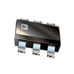
| 描述 | IC OPAMP VIDEO SINGLE SC70-6 |
| 产品分类 | |
| 品牌 | Analog Devices Inc |
| 数据手册 | |
| 产品图片 |
|
| 产品型号 | ADA4853-1AKSZ-R7 |
| rohs | 无铅 / 符合限制有害物质指令(RoHS)规范要求 |
| 产品系列 | - |
| 供应商器件封装 | SC-70-6 |
| 其它名称 | ADA4853-1AKSZ-R7-ND |
| 包装 | 带卷 (TR) |
| 压摆率 | 120 V/µs |
| 安装类型 | 表面贴装 |
| 封装/外壳 | 6-TSSOP,SC-88,SOT-363 |
| 应用 | 电压反馈 |
| 标准包装 | 3,000 |
| 电压-电源,单/双 (±) | 2.65 V ~ 5 V |
| 电流-电源 | 1.4mA |
| 电流-输出/通道 | 160mA |
| 电路数 | 1 |
| 输出类型 | 满摆幅 |


- 商务部:美国ITC正式对集成电路等产品启动337调查
- 曝三星4nm工艺存在良率问题 高通将骁龙8 Gen1或转产台积电
- 太阳诱电将投资9.5亿元在常州建新厂生产MLCC 预计2023年完工
- 英特尔发布欧洲新工厂建设计划 深化IDM 2.0 战略
- 台积电先进制程称霸业界 有大客户加持明年业绩稳了
- 达到5530亿美元!SIA预计今年全球半导体销售额将创下新高
- 英特尔拟将自动驾驶子公司Mobileye上市 估值或超500亿美元
- 三星加码芯片和SET,合并消费电子和移动部门,撤换高东真等 CEO
- 三星电子宣布重大人事变动 还合并消费电子和移动部门
- 海关总署:前11个月进口集成电路产品价值2.52万亿元 增长14.8%


PDF Datasheet 数据手册内容提取
Low Power, Rail-to-Rail Output, Video Op Amps with Ultralow Power Data Sheet ADA4853-1/ADA4853-2/ADA4853-3 FEATURES PIN CONFIGURATIONS Qualified for automotive applications (ADA4853-3W only) 1 E2 E LBLB Ultralow disable current: 0.1 μA AA CNCNSDISDI Low quiescent current: 1.4 mA/amplifier 61 51 41 31 Ideal for standard definition video ADA4853-2 VOUT11 12+VS High speed –IN12 – 11VOUT2 100 MHz, −3 dB bandwidth +IN13 + – 10–IN2 120 V/μs slew rate VOUT 1 ADA4853-1 6 +VS –VS4 + 9 +IN2 0.5 dB flatness: 22 MHz –VS 2 5 DISABLE 5C6C7C8C NNNN Differential gain: 0.20% +IN 3 4 –IN NOTES Differential phase: 0.10° (NToOtPtoVSIEcWale) 05884-001 12 .. NECXCOP N=ON NSEOEC DTC EODDINE NT POEAC GDTN .MDU.ST BE 05884-002 Single-supply operation Figure 1. 6-Lead SC70 Figure 2. 16-Lead LFCSP_WQ Rail-to-rail output ADA4853-3 Output swings to within 200 mV of either rail V+S3VTUO3N–I3N+I Low voltage offset: 1 mV 61 51 41 31 Wide supply range: 2.65 V to 5 V – + APPLICATIONS DDIISSAABBLLEE 1212 + 1121+–VINS2 DISABLE 1 1 14 VOUT3 DISABLE 33 – 10–IN2 DISABLE 2 2 + – 13 –IN3 AAuuttoommoottiivvee sinaffoettayi snymsteenmt ss ystems +VS4 5+ 6– 7 8 9 VOUT2 DISABL+EV 3S 43 ADA4853-3 1121 +–VINS3 PVDoiidgretitaoab lc lsaetm imlle ucrlaatmsim eeradsia players N1 . O ECTXOEPNSONSEECDT EDDIE T 1N+IPOA GD1N–IN MDV1UTUO.SV–TS BE 05884-003 VO+–UIINNT111 567 – + + – 1890 V–+IIONNU22T2 05884-004 Figure 3. 16-Lead LFCSP_WQ Figure 4. 14-Lead TSSOP Consumer video Clock buffer GENERAL DESCRIPTION The ADA4853-1/ADA4853-2/ADA4853-3 are low power, low cost, The ADA4853-1 is available in a 6-lead SC70, the ADA4853-2 is high speed, rail-to-rail output op amps with ultralow power disables available in a 16-lead LFCSP_WQ, and the ADA4853-3 is available in that are ideal for portable consumer electronics. Despite their low both a 16-lead LFCSP_WQ and a 14-lead TSSOP. The ADA4853-1 price, the ADA4853-1/ADA4853-2/ADA4853-3 provide excellent temperature range is −40°C to +85°C while the ADA4853-2/ overall performance and versatility. The 100 MHz, −3 dB ADA4853-3 temperature range is −40°C to +105°C. bandwidth, and 120 V/μs slew rate make these amplifiers well- 6.5 suited for many general-purpose, high speed applications. VS=5V 0.1Vp-p 6.4 RL=150Ω G=+2 The ADA4853-1/ADA4853-2/ADA4853-3 voltage feedback op 6.3 amps are designed to operate at supply voltages as low as 2.65 V and up B) d 6.2 to 5 V using only 1.4 mA of supply current per amplifier. To further N( AI 6.1 reduce power consumption, the amplifiers are equipped with a disable G P 2.0Vp-p mode that lowers the supply current to less than 1.5 μA maximum, OO 6.0 L making them ideal in battery-powered applications. D- 5.9 E S The ADA4853-1/ADA4853-2/ADA4853-3 provide users with a LO 5.8 C true single-supply capability, allowing input signals to extend 5.7 2ra0i0l. mOVn tbheel oowu ttphuet ,n tehgea taimvep rliafiile arns dca tno swwiitnhgin w 1i.t2h iVn o2f0 t0h me pVo osift ive 55..65 05884-010 either supply rail. With their combination of low price, excellent 0.1 1 10 40 FREQUENCY(MHz) differential gain (0.2%), differential phase (0.10°), and 0.5 dB flatness Figure 5. 0.5 dB Flatness Frequency Response out to 22 MHz, these amplifiers are ideal for video applications. Rev. G Document Feedback Information furnished by Analog Devices is believed to be accurate and reliable. However, no responsibility is assumed by Analog Devices for its use, nor for any infringements of patents or other One Technology Way, P.O. Box 9106, Norwood, MA 02062-9106, U.S.A. rights of third parties that may result from its use. Specifications subject to change without notice. No license is granted by implication or otherwise under any patent or patent rights of Analog Devices. Tel: 781.329.4700 ©2006–2014 Analog Devices, Inc. All rights reserved. Trademarks and registered trademarks are the property of their respective owners. Technical Support www.analog.com
ADA4853-1/ADA4853-2/ADA4853-3 Data Sheet TABLE OF CONTENTS Features .............................................................................................. 1 Typical Performance Characteristics ..............................................8 Applications ....................................................................................... 1 Circuit Description......................................................................... 16 Pin Configurations ........................................................................... 1 Headroom Considerations ........................................................ 16 General Description ......................................................................... 1 Overload Behavior and Recovery ............................................ 16 Revision History ............................................................................... 2 Applications Information .............................................................. 17 Specifications ..................................................................................... 3 Single-Supply Video Amplifier ................................................. 17 Specifications with 3 V Supply ................................................... 3 Power Supply Bypassing ............................................................ 17 Specifications with 5 V Supply ................................................... 5 Layout .......................................................................................... 17 Absolute Maximum Ratings ............................................................ 7 Outline Dimensions ....................................................................... 18 Thermal Resistance ...................................................................... 7 Ordering Guide .......................................................................... 19 ESD Caution .................................................................................. 7 Automotive Products ................................................................. 19 REVISION HISTORY 12/14—Rev. F to Rev. G Changes to DC Performance, Input Characteristics, and Power Supply Sections ...................................................................... 4 Updated Figure 54; Outline Dimensions ..................................... 18 Changes to Figure 20 ......................................................................... 8 Changes to Ordering Guide .......................................................... 19 Changes to Figure 49 ...................................................................... 13 1/11—Rev. E to Rev. F Updated Outline Dimensions ....................................................... 16 Changes to Features Section, Applications Section, and General Changes to Ordering Guide .......................................................... 16 Description Section .......................................................................... 1 7/06—Rev. 0 to Rev. A Changed Pin 5 to DISABLE in Figure 1 ........................................ 1 Added ADA4853-2 .............................................................. Universal Changed Pin 13 to DISABLE 2 and Pin 14 and DISABLE 1 in Changes to Features and General Description .............................. 1 Figure 2 .............................................................................................. 1 Changes to Table 1 ............................................................................. 3 Changes to Table 1 ............................................................................ 3 Changes to Table 2 ............................................................................. 4 Changes to Table 2 ............................................................................ 5 Changes to Table 3 ............................................................................. 5 Changes to Ordering Guide .......................................................... 18 Changes to Figure 7 ........................................................................... 6 Added Automotive Products Section........................................... 18 Changes to Figure 11 Caption, Figure 12, Figure 13, 9/10—Rev. D to Rev. E and Figure 16 ...................................................................................... 7 Changes to Figure 2 and Figure 3 ................................................... 1 Changes to Figure 17 and Figure 19 ............................................... 8 Inserted Figure 21; Renumbered Sequentially .............................. 8 6/10—Rev. C to Rev. D Inserted Figure 25; Renumbered Sequentially .............................. 9 Changes to Figure 2 and Figure 3 ................................................... 1 Changes to Figure 28 ......................................................................... 9 Changes to Outline Dimensions ................................................... 16 Changes to Figure 31 through Figure 35 ..................................... 10 10/07—Rev. B to Rev. C Changes to Figure 37, Figure 39 through Figure 42 .................. 11 Inserted Figure 43 and Figure 46 .................................................. 12 Changes to Applications Section .................................................... 1 Inserted Figure 47 ........................................................................... 13 Changes to Ordering Guide .......................................................... 16 Changes to Circuit Description Section ...................................... 13 10/06—Rev. A to Rev. B Changes to Headroom Considerations Section ......................... 13 Added ADA4853-3 .............................................................. Universal Changes to Figure 48 ...................................................................... 14 Added 16-Lead LFCSP_VQ .............................................. Universal Updated Outline Dimensions ....................................................... 15 Added 14-Lead TSSOP ...................................................... Universal Changes to Ordering Guide .......................................................... 15 Changes to Features .......................................................................... 1 1/06—Revision 0: Initial Version Changes to DC Performance, Input Characteristics, and Power Supply Sections ..................................................................... 3 Rev. G | Page 2 of 20
Data Sheet ADA4853-1/ADA4853-2/ADA4853-3 SPECIFICATIONS SPECIFICATIONS WITH 3 V SUPPLY T = 25°C, R = 1 kΩ, R = 1 kΩ for G = +2, R = 150 Ω, unless otherwise noted. A F G L Table 1. Parameter Conditions Min Typ Max Unit DYNAMIC PERFORMANCE −3 dB Bandwidth G = +1, V = 0.1 V p-p 90 MHz O G = +2, V = 2 V p-p 32 MHz O Bandwidth for 0.5 dB Flatness G = +2, V = 2 V p-p, R = 150 Ω 22 MHz O L Settling Time to 0.1% V = 2 V step 45 ns O Slew Rate G = +2, V = 2 V step 88 100 V/µs O ADA4853-3W only: T to T 60 V/µs MIN MAX NOISE/DISTORTION PERFORMANCE Differential Gain R = 150 Ω 0.20 % L Differential Phase R = 150 Ω 0.10 Degrees L Input Voltage Noise f = 100 kHz 22 nV/√Hz Input Current Noise f = 100 kHz 2.2 pA/√Hz Crosstalk G = +2, V = 2 V p-p, R = 150 Ω, f = 5 MHz −66 dB O L DC PERFORMANCE Input Offset Voltage 1 4.0 mV ADA4853-3W only: T to T 6.0 mV MIN MAX Input Offset Voltage Drift 1.6 µV/°C Input Bias Current 1.0 1.7 µA ADA4853-3W only: T to T 1.7 µA MIN MAX Input Bias Current Drift 4 nA/°C Input Bias Offset Current 50 nA Open-Loop Gain V = 0.5 V to 2.5 V 72 80 dB O ADA4853-3W only: T to T 69 dB MIN MAX INPUT CHARACTERISTICS Input Resistance Differential/common mode 0.5/20 MΩ Input Capacitance 0.6 pF Input Common-Mode Voltage Range −0.2 to +V − 1.2 V CC Input Overdrive Recovery Time (Rise/Fall) V = −0.5 V to +3.5 V, G = +1 40 ns IN Common-Mode Rejection Ratio V = 0 V to 1 V −69 −85 dB CM ADA4853-3W only: T to T −66 dB MIN MAX DISABLE DISABLE Input Voltage 1.2 V Turn-Off Time 1.4 µs Turn-On Time 120 ns DISABLE Bias Current Enabled DISABLE = 3.0 V 25 30 µA DISABLE = 3.0 V, ADA4853-3W only: 30 µA T to T MIN MAX Disabled DISABLE = 0 V 0.01 µA OUTPUT CHARACTERISTICS Output Overdrive Recovery Time V = −0.25 V to +1.75 V, G = +2 70 ns IN Output Voltage Swing R = 150 Ω 0.3 to 2.7 0.15 to 2.88 V L R = 150 Ω, ADA4853-3W only: T to T 0.3 to 2.7 V L MIN MAX Short-Circuit Current Sinking/sourcing 150/120 mA Rev. G | Page 3 of 20
ADA4853-1/ADA4853-2/ADA4853-3 Data Sheet Parameter Conditions Min Typ Max Unit POWER SUPPLY Operating Range 2.65 5 V Quiescent Current/Amplifier 1.3 1.6 mA ADA4853-3W only: T to T 1.6 mA MIN MAX Quiescent Current (Disabled)/Amplifier DISABLE = 0 V 0.1 1.5 µA DISABLE = 0 V, ADA4853-3W only: T to T 1.5 µA MIN MAX Positive Power Supply Rejection +V = +1.5 V to +2.5 V, −V = −1.5 V −76 −86 dB S S ADA4853-3W only: T to T −76 dB MIN MAX Negative Power Supply Rejection −V = −1.5 V to −2.5 V, +V = +1.5 V −77 −88 dB S S ADA4853-3W only: T to T −74 dB MIN MAX Rev. G | Page 4 of 20
Data Sheet ADA4853-1/ADA4853-2/ADA4853-3 SPECIFICATIONS WITH 5 V SUPPLY T = 25°C, R = 1 kΩ, R = 1 kΩ for G = +2, R = 150 Ω, unless otherwise noted. A F G L Table 2. Parameter Conditions Min Typ Max Unit DYNAMIC PERFORMANCE −3 dB Bandwidth G = +1, V = 0.1 V p-p 100 MHz O G = +2, V = 2 V p-p 35 MHz O Bandwidth for 0.5 dB Flatness G = +2, V = 2 V p-p 22 MHz O Settling Time to 0.1% V = 2 V step 54 ns O Slew Rate G = +2, V = 2 V step 93 120 V/µs O ADA4853-3W only: T to T 70 V/µs MIN MAX NOISE/DISTORTION PERFORMANCE Differential Gain R = 150 Ω 0.22 % L Differential Phase R = 150 Ω 0.10 Degrees L Input Voltage Noise f = 100 kHz 22 nV/√Hz Input Current Noise f = 100 kHz 2.2 pA/√Hz Crosstalk G = +2, V = 2 V p-p, R = 150 Ω, f = 5 MHz −66 dB O L DC PERFORMANCE Input Offset Voltage 1 4.1 mV ADA4853-3W only: T to T 6.0 mV MIN MAX Input Offset Voltage Drift 1.6 µV/°C Input Bias Current 1.0 1.7 µA ADA4853-3W only: T to T 1.7 µA MIN MAX Input Bias Current Drift 4 nA/°C Input Bias Offset Current 60 nA Open-Loop Gain V = 0.5 V to 4.5 V 72 80 dB O ADA4853-3W only: T to T 70 dB MIN MAX INPUT CHARACTERISTICS Input Resistance Differential/common mode 0.5/20 MΩ Input Capacitance 0.6 pF Input Common-Mode Voltage Range −0.2 to +V − 1.2 V CC Input Overdrive Recovery Time V = −0.5 V to +5.5 V, G = +1 40 ns IN (Rise/Fall) Common-Mode Rejection Ratio V = 0 V to 3 V −71 −88 dB CM ADA4853-3W only: T to T −68 dB MIN MAX DISABLE DISABLE Input Voltage 1.2 V Turn-Off Time 1.5 µs Turn-On Time 120 ns DISABLE Bias Current Enabled DISABLE = 5 V 40 50 µA DISABLE = 5 V, ADA4853-3W only: 50 µA T to T MIN MAX Disabled DISABLE = 0 V 0.01 µA OUTPUT CHARACTERISTICS Output Overdrive Recovery Time V = −0.25 V to +2.75 V, G = +2 55 ns IN Output Voltage Swing R = 75 Ω 0.55 to 4.5 0.1 to 4.8 V L R = 75 Ω, ADA4853-3W only: T to T 0.55 to 4.5 V L MIN MAX Short-Circuit Current Sinking/sourcing 160/120 mA Rev. G | Page 5 of 20
ADA4853-1/ADA4853-2/ADA4853-3 Data Sheet Parameter Conditions Min Typ Max Unit POWER SUPPLY Operating Range 2.65 5 V Quiescent Current/Amplifier 1.4 1.8 mA ADA4853-3W only: T to T 1.8 mA MIN MAX Quiescent Current (Disabled)/Amplifier DISABLE = 0 V 0.1 1.5 µA DISABLE = 0 V, ADA4853-3W only: T to 1.5 µA MIN T MAX Positive Power Supply Rejection +V = +2.5 V to +3.5 V, −V = −2.5 V −75 −80 dB S S ADA4853-3W only: T to T −72 MIN MAX Negative Power Supply Rejection −V = −2.5 V to −3.5 V, +V = +2.5 V −75 −80 dB S S ADA4853-3W only: T to T −72 dB MIN MAX Rev. G | Page 6 of 20
Data Sheet ADA4853-1/ADA4853-2/ADA4853-3 ABSOLUTE MAXIMUM RATINGS The power dissipated in the package (P ) for a sine wave and a Table 3. D resistor load is the total power consumed from the supply Parameter Rating minus the load power. Supply Voltage 5.5 V Power Dissipation See Figure 6 PD = Total Power Consumed − Load Power Common-Mode Input Voltage −VS − 0.2 V to +VS − 1.2 V ( ) V 2 Differential Input Voltage ±V P = V ×I – OUT S D SUPPLYVOLTAGE SUPPLYCURRENT R Storage Temperature Range −65°C to +125°C L Operating Temperature Range RMS output voltages should be considered. 6-Lead SC70 −40°C to +85°C Airflow increases heat dissipation, effectively reducing θ . JA 16-Lead LFCSP_WQ −40°C to +105°C In addition, more metal directly in contact with the package 14-Lead TSSOP −40°C to +105°C leads and through holes under the device reduces θ . JA Lead Temperature JEDEC J-STD-20 Figure 6 shows the maximum safe power dissipation in the Junction Temperature 150°C package vs. the ambient temperature for the 6-lead SC70 Stresses above those listed under Absolute Maximum Ratings (430°C/W), the 14-lead TSSOP (120°C/W), and the 16-lead may cause permanent damage to the device. This is a stress LFCSP_WQ (63°C/W) on a JEDEC standard 4-layer board. θJA rating only; functional operation of the device at these or any values are approximations. other conditions above those indicated in the operational 3.0 section of this specification is not implied. Exposure to absolute maximum rating conditions for extended periods may affect W) 2.5 N ( device reliability. O TI THERMAL RESISTANCE SSIPA 2.0 LFCSP DI θJA is specified for the worst-case conditions, that is, θJA is R 1.5 E specified for the device soldered in the circuit board for OW TSSOP P surface-mount packages. M 1.0 U M Table 4. AXI M 0.5 Package Type θ Unit JA SC70 6-Lead SC70 430 °C/W 0 1164--LLeeaadd TLSFSCOSPP_ WQ 16230 °°CC//WW –55 –35 –15AMBI5ENT T2E5MPER45ATUR6E5 (°C)85 105 125 05884-059 Figure 6. Maximum Power Dissipation vs. Temperature for a 4-Layer Board Maximum Power Dissipation ESD CAUTION The maximum safe power dissipation for the ADA4853-1/ ADA4853-2/ADA4853-3 is limited by the associated rise in junction temperature (T) on the die. At approximately 150°C, J which is the glass transition temperature, the plastic changes its properties. Even temporarily exceeding this temperature limit can change the stresses that the package exerts on the die, permanently shifting the parametric performance of the amplifiers. Exceeding a junction temperature of 150°C for an extended period can result in changes in silicon devices, potentially causing degradation or loss of functionality. Rev. G | Page 7 of 20
ADA4853-1/ADA4853-2/ADA4853-3 Data Sheet TYPICAL PERFORMANCE CHARACTERISTICS 2 5 ADA4853-3 VS = 5V CL = 10pF/25Ω SNUB dB) 1 LFCSP 4 VROL U=T 1 =5 00Ω.1V p-p CL = 10pF GAIN ( 0 G = –1* B) 32 G = +1 CL = 5pF OOP –1 G = +2* AIN (d 1 CLOSED-L –2 G = +10* D-LOOP G –10 CL = 0pF ALIZED ––34 *ADA4853-1/ADA4853-2 CLOSE ––32 RSNUB RM –4 NO –5 VRSL == 51V50Ω –5 CL RL VOUT = 0.1V p-p –60.1 1 FREQUENCY (M1H0z) 100 200 05884-006 –60.1 1 FREQUENCY (M1H0z) 100 200 05884-009 Figure 7. Small Signal Frequency Response for Various Gains Figure 10. Small Signal Frequency Response for Various Capacitive Loads 3 6.5 2 VGS = = + 51V RL = 75Ω 6.4 VRSL==51V50Ω 0.1Vp-p VOUT = 0.1V p-p G=+2 6.3 1 B) B) d d 6.2 AIN( 0 RL = 1kΩ AIN( 6.1 G G OP –1 RL = 150Ω OP 6.0 2.0Vp-p O O L –2 L D- D- 5.9 E E LOS –3 LOS 5.8 C C –4 5.7 –5 5.6 –60.1 1 FREQUENCY(M1H0z) 100 200 05884-007 5.50.1 FR1EQUENCY(MHz) 10 40 05884-010 Figure 8. Small Signal Frequency Response for Various Loads Figure 11. 0.5 dB Flatness Response for Various Output Voltages 4 8.0 G = +1 VS = 3V VS = 5V 3 RL = 150Ω 7.8 RGL = = + 1250Ω VOUT = 0.1V p-p 7.6 2 N(dB) 1 VS = 5V N (dB) 77..42 0.1V p-p AI 0 AI 7.0 G G OP –1 OP 6.8 O O L L 6.6 D- –2 D- SE SE 6.4 CLO –3 CLO 6.2 –4 6.0 2V p-p –5 5.8 5.6 –60.1 1 FREQUENCY(M1H0z) 100 200 05884-008 0.1 1 FREQUE1N0CY (MHz) 100 1000 05884-060 Figure 9. Small Signal Frequency Response for Various Supplies Figure 12. ADA4853-3 LFCSP_WQ Flatness Response for Various Output Voltages Rev. G | Page 8 of 20
Data Sheet ADA4853-1/ADA4853-2/ADA4853-3 1 4 dB) 0 G=–1 3 VRVSOL U==T 51 =V5 00Ω.1V p-p +25°C +85°C ( G = +1 N G=+2 2 PGAI –1 G=+10 (dB) 1 O N OSED-LO –2 OOP GAI –10 –40°C CL –3 D-L –2 ALIZED –4 CLOSE –3 RM –4 NO –5 VS = 5V RL = 150Ω –5 –60.1VOUT = 2V p-p 1 FREQUENCY(M1H0z) 100 200 05884-011 –60.1 1 FREQUENCY (M1H0z) 100 200 05884-014 Figure 13. Large Signal Frequency Response for Various Gains Figure 16. Small Signal Frequency Response for Various Temperatures 7 250 VS=5V RL=150Ω 6 G=+2 200 dB) 5 RL=75Ω RL=1kΩ NEGATIVESLEWRATE AIN( RL=150Ω V/µs) 150 D-LOOPG 43 W RATE( 100 POSITIVESLEWRATE E E OS SL L 2 C 50 1 VS=5V VOUT=2Vp-p G=+2 00.1 1 FREQUENCY(M1H0z) 100 200 05884-012 00 0.5 1.0OUTP1U.5TVOL2T.0AGES2T.5EP(V)3.0 3.5 4.0 05884-015 Figure 14. Large Signal Frequency Response for Various Loads Figure 17. Slew Rate vs. Output Voltage 5 140 0 VS = 3V +85°C VS=5V 4 RL = 150Ω +25°C RL=150Ω VOUT = 0.1V p-p 120 –30 3 G = +1 s) OOP GAIN (dB) 210 –40°C OP GAIN (dB)1086000 PHASE –––1962000 PHASE (Degree CLOSED-L –––123 OPEN-LO 4200 GAIN ––118500 PEN-LOOP O –4 0 –210 –5 –60.1 1 FREQUENCY(M1H0z) 100 200 05884-013 –20100 1k 10kFREQ1U00EkNCY(H1zM) 10M 100M –240 05884-029 Figure 15. Small Signal Frequency Response for Various Temperatures Figure 18. Open-Loop Gain and Phase vs. Frequency Rev. G | Page 9 of 20
ADA4853-1/ADA4853-2/ADA4853-3 Data Sheet –20 10M VS = 5V VS = 5V TION (dB) ––4300 PEDANCE (Ω) 1010Mk G = +1 AADDAA44885533--12/ ODE REJEC ––6500 OUTPUT IM 10k ADA4853-3 M P MMON- –70 D-LOO 1k CO –80 OSE 100 –90 05884-030 CL 10 100 1k 10k FREQ10U0EkNCY (H1zM) 10M 100M 100 1k 10kFREQ1U0E0kNCY (H1z)M 10M 100M 05884-050 Figure 19. Common-Mode Rejection vs. Frequency Figure 22. Output Impedance vs. Frequency Disabled 0 –40 VS = 5V G = +2 –10 GAIN = +2 VS = 3V RTO –50 VOUT = 2V p-p dB) –20 c) RL = 150Ω HD2 ON ( –30 –PSR (dB –60 RL = 150Ω HD3 ECTI –40 TION J R –70 E O PPLY R ––5600 +PSR CDIST –80 RL = 1kΩ HD3 SU ONI RL = 1kΩ HD2 R –70 M –90 E R W A O –80 H P –100 –90 –100100 1k 10k FREQ10U0EkNCY (H1zM) 10M 100M 05884-031 –1100.1 FREQUEN1CY (MHz) 10 05884-016 Figure 20. Power Supply Rejection vs. Frequency Figure 23. Harmonic Distortion vs. Frequency 1000 –40 VS = 5V G = +2 T IMPEDANCE (Ω) 10100 G = +1 RTION(dBc) –––576000 VVSO U=T 5 =V 2V p-p RL = 150Ω HDR2L = 150Ω HD3 TPU STO –80 RL = 1kΩ HD3 OP OU 1 NICDI –90 O O SED-L 0.1 HARM –100 RL = 1kΩ HD2 O CL0.01100 1k 10k FREQ10U0EkNCY (H1zM) 10M 100M 05884-032 ––1121000.1 FREQUEN1CY (MHz) 10 05884-017 Figure 21. Output Impedance vs. Frequency Enabled Figure 24. Harmonic Distortion vs. Frequency Rev. G | Page 10 of 20
Data Sheet ADA4853-1/ADA4853-2/ADA4853-3 –40 2.60 G = +1 G = +2 –50 VVSO U=T 5 =V 2V p-p RL = 150Ω HD3 2.58 R25Ln =s /1D5I0VΩ VS = 3V c) 2.56 B –60 RTION(d –70 RL = 75Ω HD2 RL = 150Ω HD2 AGE (V) 22..5524 VS = 5V DISTO –80 RL = 75Ω HD3 T VOLT 2.50 C U 2.48 MONI –90 OUTP 2.46 AR –100 H RL = 1kΩ HD2 2.44 ––1121000.1 FREQUEN1CY (MHz) RL = 1kΩ HD3 10 05884-018 22..4402 05884-033 Figure 25. Harmonic Distortion vs. Frequency Figure 28. Small Signal Pulse Response for Various Supplies –30 2.60 G=+2 VOUT=2Vp-p 2.58 –40 RL=75Ω G=+1;CL=5pF c) 2.56 B C DISTORTION (d –––567000 VS=3VHD2 VS=3VHD3 VS=5VHD2 UT VOLTAGE (V) 2222....45558024 G=+2;CL=0pF,5pF,10pF RMONI –80 VS=5VHD3 OUTP 2.46 A H 2.44 –90 VS=5V –1000.1 FREQUEN1CY(MHz) 10 05884-051 22..4402 R25Ln=s/1D5I0VΩ 05884-034 Figure 26. Harmonic Distortion vs. Frequency Figure 29. Small Signal Pulse Response for Various Capacitive Loads –40 3.75 G = +1 G = +2 –50 RfV =SL 1==0 510V5k0HΩz 5V 3.50 R25Ln =s /1D5I0VΩ VS = 3V, 5V Bc) –60 2V 3.25 RTION(d –70 GND AGE (V) 23..7050 DISTO –80 T VOLT 2.50 C U 2.25 MONI –90 OUTP 2.00 AR –100 H HD2 1.75 ––112100 HD3 05884-019 11..2550 05884-035 0 1 2 3 4 VOUT (V p-p) Figure 27. Harmonic Distortion for Various Output Voltages Figure 30. Large Signal Pulse Response for Various Supplies Rev. G | Page 11 of 20
ADA4853-1/ADA4853-2/ADA4853-3 Data Sheet 3.75 1000 G = +2 3.50 VS = 5V RL = 150Ω 3.25 25ns/DIV OLTAGE (V) 223...570050 CL = 0pF, 20pF OISE (nV/ Hz)100 V N T E PU 2.25 AG OUT 2.00 OLT V 1.75 11..2550 05884-036 1010 100 1k FREQ1U0EkNCY(H10z0)k 1M 10M 05884-037 Figure 31. Large Signal Pulse Response for Various Capacitive Loads Figure 34. Voltage Noise vs. Frequency 5.5 100 2×INPUT VS=5V G=+2 V) 4.5 Rf=L1=M1H50zΩ AGE ( OUTPUT Hz) LT 3.5 A/ O p PUT V 2.5 OISE ( 10 T N D OU ENT AN 1.5 RR UT CU P IN 0.5 –0.5 100ns/DIV 05884-020 110 100 1k FREQ1U0EkNCY(H10z0)k 1M 10M 05884-038 Figure 32. Output Overdrive Recovery Figure 35. Current Noise vs. Frequency 5.5 20 V) 4.5 INPUT VGRf=SL=1==+M511HV50zΩ 18 VNx S == = –1 055.V5370mV GE ( OUTPUT 16 σ = 0.782 A 14 LT 3.5 O V 12 T T U N P 2.5 U 10 T O U C D O 8 T AN 1.5 6 U INP 0.5 4 2 –0.5 100ns/DIV 05884-021 0–4 –3 –2 –1 VOS 0(mV) 1 2 3 4 05884-042 Figure 33. Input Overdrive Recovery Figure 36. VOS Distribution Rev. G | Page 12 of 20
Data Sheet ADA4853-1/ADA4853-2/ADA4853-3 –0.6 –0.50 VS = 5V –0.52 –0.8 –0.54 –1.0 µA) VS=5V T ( –0.56 N E V (mV)OS ––11..24 AS CURR ––00..5680 +IB BI UT –0.62 VS=3V –1.6 P N I –0.64 –IB –1.8 –0.66 –2.0–1.0 –0.5 0 0.5 1.0 1V.5CM (2V.0) 2.5 3.0 3.5 4.0 4.5 05884-022 –0.68–40 –20 0TEMPER2A0TURE(°4C0) 60 80 05884-027 Figure 37. VOS vs. Common-Mode Voltage Figure 40. Input Bias Current vs. Temperature 1.5 3.0 VS=5V,T=+85°C VS=3V 2.8 POSITIVESWING LOADRESISTANCETIED TOMIDSUPPLY VS=5V,T=–40°C RRENT (mA) 1.0 VS=3VVS,=T3=V+,2T5°=CV–S40=°C5V,T=+25°C OLTAGE (V) 22..64 Y CU VS=3V,T=+85°C UT V 0.6 PPL 0.5 UTP 0.4 U O S 0.2 NEGATIVESWING 00 0.5 1.0 P1O.5WER2.D0OW2N.5VOL3T.0AGE3(.V5) 4.0 4.5 5.0 05884-023 01 10 LOADRES1I0S0TANCE(Ω) 1k 10k 05884-039 Figure 38. Supply Current vs. POWER DOWN Voltage Figure 41. Output Voltage vs. Load Resistance –0.6 5.0 VS=5V LOADRESISTANCETIED 4.8 POSITIVESWING TOMIDSUPPLY V) VS = 5V m –0.7 FFSET VOLTAGE ( –0.8 VS = 3V PUT VOLTAGE (V) 440...646 UT O OUT 0.4 P –0.9 N I 0.2 –1.0–50 –25 0TEMPERA25TURE (°C5)0 75 10005884-026 010 NEGATIVES1LW0O0IANDGRESISTANCE(1Ωk) 10k 05884-040 Figure 39. Input Offset Voltage vs. Temperature Figure 42. Output Voltage vs. Load Resistance Rev. G | Page 13 of 20
ADA4853-1/ADA4853-2/ADA4853-3 Data Sheet 3.0 0.25 VS=3V RL=150Ω 2.9 2.8 E (V) 0.20 +VSAT POSITIVESWING G VS=5V V) 2.7 TA E ( OL OLTAG 22..65 TION V 0.15 V 0.5 A UTPUT 0.4 SATUR 0.10 VS=3V –VSAT O 0.3 T U NEGATIVESWING P 0.2 UT 0.05 O 0.1 0 0 0 5 10 15LOA2D0CUR25RENT30(mA)35 40 45 50 05884-041 –40 –20 0TEMPER2A0TURE(°4C0) 60 80 05884-053 Figure 43. Output Voltage vs. Load Current Figure 45. Output Saturation Voltage vs. Temperature for Various Supplies 5.0 3.0 4.9 VS=5V 3.1 VRSL==51V50Ω VOUTPUT 2.9 4.8 POSITIVESWING 2.8 2VINPUT V) 4.7 OUTPUT VOLTAGE ( 44000.....65543 VOLTAGE (V) 22222.....45673 2VINPUT–VOUTPUT (–+(–+0000..0.0.1100%%11))2VV(V)INPUT –OUTPUT NEGATIVESWING 2.2 0.2 2.1 0.1 2.0 00 5 10 15LOA2D0CUR25RENT30(mA)35 40 45 50 05884-052 1.90 10 20 30 40 50 60TI7M0E(8n0s)90 100110120130140150 05884-045 Figure 44. Output Voltage vs. Load Current Figure 46. 0.1% Settling Time Rev. G | Page 14 of 20
Data Sheet ADA4853-1/ADA4853-2/ADA4853-3 6 3 0 POWER DOWN VS = 5V RL = 150Ω E (V) 5 ADAVO48U5T3-3 N (dB) –20 VGI N= =+ 21V p-p N PIN VOLTAG 43 AA DD AA V44O88U55T33--12/ 2 VOLTAGE(V) PUT ISOLATIO –40 R DOW 2 1 UTPUT O-OUT –60 WE 1 O T-T PO 0 G = +2 0 INPU –80 VS = 5V fIN = 100kHz –10 1 2 3 4 TIME5 (µs)6 7 8 9 10 05884-046 –1000.1 1 FREQUENCY (M1H0z) 100 200 05884-055 Figure 47. Enable/Disable Time Figure 49. Input-to-Output Isolation, Chip Disabled –40 VS = 5V G = +2 –50 RVOL U=T 1 =5 02ΩV p-p B) –60 K (d VO AUTD2A T4O85 V3O-2UT1 L TA –70 S S RO VOUT1 TO VOUT2 C –80 ADA4853-2 ADA4853-3 –90 ALL HOSTILE –100 100k 1M FREQUENCY 1(H0Mz) 100M200M 05884-054 Figure 48. Crosstalk vs. Frequency Rev. G | Page 15 of 20
ADA4853-1/ADA4853-2/ADA4853-3 Data Sheet CIRCUIT DESCRIPTION The ADA4853-1/ADA4853-2/ADA4853-3 feature a high slew For signals approaching the negative supply, inverting gain, and rate input stage that is a true single-supply topology capable of high positive gain configurations, the headroom limit is the sensing signals at or below the minus supply rail. The rail-to- output stage. The ADA4853-1/ADA4853-2/ADA4853-3 use a rail output stage can pull within 100 mV of either supply rail common-emitter output stage. This output stage maximizes the when driving light loads and within 200 mV when driving available output range, limited by the saturation voltage of the 150 Ω. High speed performance is maintained at supply output transistors. The saturation voltage increases with the voltages as low as 2.65 V. drive current that the output transistor is required to supply due HEADROOM CONSIDERATIONS to the collector resistance of the output transistor. As the saturation point of the output stage is approached, the The ADA4853-1/ADA4853-2/ADA4853-3 are designed for use in output signal shows increasing amounts of compression and low voltage systems. To obtain optimum performance, it is clipping. For the input headroom case, higher frequency signals useful to understand the behavior of the amplifiers as input and require a bit more headroom than the lower frequency signals. output signals approach their headroom limits. The input Figure 27 illustrates this point by plotting the typical distortion common-mode voltage range of the amplifier extends from the vs. the output amplitude. negative supply voltage (actually 200 mV below this) to within 1.2 V of the positive supply voltage. OVERLOAD BEHAVIOR AND RECOVERY Exceeding the headroom limits is not a concern for any Input inverting gain on any supply voltage, as long as the reference The specified input common-mode voltage of the ADA4853-1/ voltage at the positive input of the amplifier lies within the a ADA4853-2/ADA4853-3 is 200 mV below the negative supply to input common-mode range of the amplifier. within 1.2 V of the positive supply. Exceeding the top limit results The input stage is the headroom limit for signals approaching in lower bandwidth and increased rise time. Pushing the input the positive rail. Figure 50 shows a typical offset voltage vs. the voltage of a unity-gain follower to less than 1.2 V from the input common-mode voltage for the ADA4853-1/ADA4853-2/ positive supply leads to an increasing amount of output error as ADA4853-3 on a 5 V supply. Accurate dc performance is well as increased settling time. The recovery time from input maintained from approximately 200 mV below the negative voltages 1.2 V or closer to the positive supply is approximately supply to within 1.2 V of the positive supply. For high speed 40 ns; this is limited by the settling artifacts caused by transis- signals, however, there are other considerations. As the tors in the input stage coming out of saturation. common-mode voltage gets within 1.2 V of positive supply, the The amplifiers do not exhibit phase reversal, even for input amplifier responds well but the bandwidth begins to drop as the voltages beyond the voltage supply rails. Going more than 0.6 V common-mode voltage approaches the positive supply. This can beyond the power supplies turns on protection diodes at the manifest itself in increased distortion or settling time. Higher input stage, greatly increasing the current draw of the devices. frequency signals require more headroom than the lower frequencies to maintain distortion performance. –0.6 VS = 5V –0.8 –1.0 V) –1.2 m (S O V –1.4 –1.6 –1.8 –2.0–1.0 –0.5 0 0.5 1.0 1V.5CM (2V.0) 2.5 3.0 3.5 4.0 4.5 05884-022 Figure 50. VOS vs. Common-Mode Voltage, VS = 5 V Rev. G | Page 16 of 20
Data Sheet ADA4853-1/ADA4853-2/ADA4853-3 APPLICATIONS INFORMATION SINGLE-SUPPLY VIDEO AMPLIFIER LAYOUT With low differential gain and phase errors and wide 0.5 dB As is the case with all high speed applications, careful attention flatness, the ADA4853-1/ADA4853-2/ADA4853-3 are ideal to printed circuit board (PCB) layout details prevents associated solutions for portable video applications. Figure 51 shows a board parasitics from becoming problematic. The ADA4853-1/ typical video driver set for a noninverting gain of +2, where ADA4853-2/ADA4853-3 can operate at up to 100 MHz; there- R = R = 1 kΩ. The video amplifier input is terminated into a fore, proper RF design techniques must be employed. The PCB F G shunt 75 Ω resistor. At the output, the amplifier has a series should have a ground plane covering all unused portions of the 75 Ω resistor for impedance matching to the video load. component side of the board to provide a low impedance return path. Removing the ground plane on all layers from the area When operating in low voltage, single-supply applications, the near and under the input and output pins reduces stray capacit- input signal is only limited by the input stage headroom. ance. Signal lines connecting the feedback and gain resistors RF should be kept as short as possible to minimize the inductance +VS 2.C21µF and stray capacitance associated with these traces. Termination + resistors and loads should be located as close as possible to their respective inputs and outputs. Input and output traces should RG PD 0.0C12µF 75Ω 75Ω CABLE VOUT be kept as far apart as possible to minimize coupling (crosstalk) U1 through the board. Adherence to microstrip or stripline design VIN V 75Ω 05884-043 treecchonmiqmueens dfoedr .l oFnogr msigonrea li ntrfaocrems a(gtiroena toenr thhiagnh 1s pineecdh )b iosa rd Figure 51. Video Amplifier layout, go to www.analog.com to view A Practical Guide to POWER SUPPLY BYPASSING High-Speed Printed-Circuit-Board Layout. Attention must be paid to bypassing the power supply pins of the ADA4853-1/ADA4853-2/ADA4853-3. High quality capacitors with low equivalent series resistance (ESR), such as multilayer ceramic capacitors (MLCCs), should be used to minimize supply voltage ripple and power dissipation. A large, usually tantalum, 2.2 µF to 47 µF capacitor located in proximity to the ADA4853-1/ADA4853-2/ADA4853-3 is required to provide good decoupling for lower frequency signals. The actual value is determined by the circuit transient and frequency requirements. In addition, 0.1 µF MLCC decoupling capacitors should be located as close to each of the power supply pins as is physically possible, no more than ⅛ inch away. The ground returns should terminate immediately into the ground plane. Locating the bypass capacitor return close to the load return minimizes ground loops and improves performance. Rev. G | Page 17 of 20
ADA4853-1/ADA4853-2/ADA4853-3 Data Sheet OUTLINE DIMENSIONS 2.20 2.00 1.80 1.35 6 5 4 2.40 1.25 2.10 1.15 1 2 3 1.80 0.65BSC 1.30BSC 1.00 1.10 0.40 0.90 0.80 0.10 0.70 0.46 0.10MAX 0.30 SPELAATNIENG 00..2028 0.36 COPLANARITY 0.15 0.26 0.10 COMPLIANTTOJEDECSTANDARDSMO-203-AB 072809-A Figure 52. 6-Lead Thin Shrink Small Outline Transistor Package [SC70] (KS-6) Dimensions shown in millimeters 5.10 5.00 4.90 14 8 4.50 4.40 6.40 BSC 4.30 1 7 PIN 1 0.65 BSC 1.05 1.00 1M.2A0X 0.20 0.80 0.09 0.75 0.15 8° 0.60 0.05 0.30 SPELAATNIENG 0° 0.45 COPLANARITY 0.19 0.10 COMPLIANT TO JEDEC STANDARDS MO-153-AB-1 061908-A Figure 53. 14-Lead Thin Shrink Small Outline Package [TSSOP] (RU-14) Dimensions shown in millimeters Rev. G | Page 18 of 20
Data Sheet ADA4853-1/ADA4853-2/ADA4853-3 3.10 0.30 3.00 SQ 0.25 PIN 1 2.90 0.20 INDICATOR PIN 1 0.50 13 16 INDICATOR BSC 12 1 EXPOSED 1.65 PAD 1.50 SQ 1.45 9 4 0.50 8 5 0.20 MIN TOP VIEW 0.40 BOTTOM VIEW 0.30 0.80 FOR PROPER CONNECTION OF 0.75 0.05 MAX THE EXPOSED PAD, REFER TO 0.70 THE PIN CONFIGURATION 0.02 NOM SECTION OF THIS DATA SHEET. COPLANARITY SEATING 0.08 PLANE 0.20 REF COMPLIANTTOJEDEC STANDARDS MO-220-WEED-6. 01-26-2012-A Figure 54. 16-Lead Lead Frame Chip Scale Package [LFCSP_WQ] 3 mm × 3 mm Body, Very Very Thin Quad (CP-16-27) Dimensions shown in millimeters ORDERING GUIDE Temperature Ordering Package Model1, 2 Range Package Description Quantity Option Branding ADA4853-1AKSZ-R2 −40°C to +85°C 6-Lead Thin Shrink Small Outline Transistor Package (SC70) 250 KS-6 HEC ADA4853-1AKSZ-R7 −40°C to +85°C 6-Lead Thin Shrink Small Outline Transistor Package (SC70) 3000 KS-6 HEC ADA4853-1AKSZ-RL −40°C to +85°C 6-Lead Thin Shrink Small Outline Transistor Package (SC70) 10,000 KS-6 HEC ADA4853-1AKS-EBZ Evaluation Board 1 ADA4853-2YCPZ-R2 −40°C to +105°C 16-Lead Lead Frame Chip Scale Package (LFCSP_WQ) 250 CP-16-27 H0H ADA4853-2YCPZ-RL −40°C to +105°C 16-Lead Lead Frame Chip Scale Package (LFCSP_WQ) 5000 CP-16-27 H0H ADA4853-2YCPZ-RL7 −40°C to +105°C 16-Lead Lead Frame Chip Scale Package (LFCSP_WQ) 1500 CP-16-27 H0H ADA4853-2YCP-EBZ Evaluation Board 1 ADA4853-3YCPZ-R2 −40°C to +105°C 16-Lead Lead Frame Chip Scale Package (LFCSP_WQ) 250 CP-16-27 H0L ADA4853-3YCPZ-RL −40°C to +105°C 16-Lead Lead Frame Chip Scale Package (LFCSP_WQ) 5000 CP-16-27 H0L ADA4853-3YCPZ-R7 −40°C to +105°C 16-Lead Lead Frame Chip Scale Package (LFCSP_WQ) 1500 CP-16-27 H0L ADA4853-3WYCPZ-R7 −40°C to +105°C 16-Lead Lead Frame Chip Scale Package (LFCSP_WQ) 1500 CP-16-27 H2H ADA4853-3YCP-EBZ Evaluation Board ADA4853-3YRUZ −40°C to +105°C 14-Lead Thin Shrink Small Outline Package (TSSOP) 96 RU-14 ADA4853-3YRUZ-RL −40°C to +105°C 14-Lead Thin Shrink Small Outline Package (TSSOP) 2500 RU-14 ADA4853-3YRUZ-R7 −40°C to +105°C 14-Lead Thin Shrink Small Outline Package (TSSOP) 1000 RU-14 ADA4853-3YRU-EBZ Evaluation Board 1 1 Z = RoHS Compliant Part. 2 W = Qualified for Automotive Applications. AUTOMOTIVE PRODUCTS The ADA4853-3W model is available with controlled manufacturing to support the quality and reliability requirements of automotive applications. Note that these automotive models may have specifications that differ from the commercial models; therefore, designers should review the Specifications section of this data sheet carefully. Only the automotive grade products shown are available for use in automotive applications. Contact your local Analog Devices account representative for specific product ordering information and to obtain the specific Automotive Reliability reports for these models. Rev. G | Page 19 of 20
ADA4853-1/ADA4853-2/ADA4853-3 Data Sheet NOTES ©2006–2014 Analog Devices, Inc. All rights reserved. Trademarks and registered trademarks are the property of their respective owners. D05884-0-12/14(G) Rev. G | Page 20 of 20
Mouser Electronics Authorized Distributor Click to View Pricing, Inventory, Delivery & Lifecycle Information: A nalog Devices Inc.: ADA4853-3YRUZ ADA4853-1AKSZ-R7 ADA4853-1AKSZ-RL ADA4853-2YCPZ-RL ADA4853-2YCPZ-RL7 ADA4853-3YCPZ-R7 ADA4853-3YCPZ-RL ADA4853-3YRUZ-R7 ADA4853-3YRUZ-RL ADA4853-2YCP-EBZ ADA4853-3YRU-EBZ ADA4853-1AKSZ-R2 ADA4853-2YCPZ-R2 ADA4853-3YCPZ-R2 ADA4853-3WYCPZ-R7