ICGOO在线商城 > 集成电路(IC) > 线性 - 放大器 - 视频放大器和频缓冲器 > THS7347IPHP
 Datasheet下载
- 型号: THS7347IPHP
- 制造商: Texas Instruments
- 库位|库存: xxxx|xxxx
- 要求:
| 数量阶梯 | 香港交货 | 国内含税 |
| +xxxx | $xxxx | ¥xxxx |
查看当月历史价格
查看今年历史价格
THS7347IPHP产品简介:
ICGOO电子元器件商城为您提供THS7347IPHP由Texas Instruments设计生产,在icgoo商城现货销售,并且可以通过原厂、代理商等渠道进行代购。 THS7347IPHP价格参考¥26.00-¥48.30。Texas InstrumentsTHS7347IPHP封装/规格:线性 - 放大器 - 视频放大器和频缓冲器, Video Amp, 3 Buffer 48-HTQFP (7x7)。您可以下载THS7347IPHP参考资料、Datasheet数据手册功能说明书,资料中有THS7347IPHP 详细功能的应用电路图电压和使用方法及教程。
THS7347IPHP 是 Texas Instruments(德州仪器)生产的一款视频放大器和频率缓冲器,属于线性放大器类别。该器件主要用于处理高清视频信号,具有多通道输出能力,适用于需要高质量视频信号传输与分配的场合。

其主要应用场景包括:

1. 视频监控系统:用于增强摄像头输出的视频信号,确保在长距离传输中保持清晰度和稳定性。
2. 专业视频设备:如视频切换器、分配放大器、视频矩阵等设备中,作为信号缓冲和驱动使用。
3. 广播与电视制作设备:用于处理SDI、HDMI等高清视频接口中的模拟或数字视频信号,确保信号完整性。
4. 医疗成像设备:如超声波、内窥镜等设备中的视频信号调理和显示输出。
5. 工业视觉与检测系统:用于图像采集与显示环节,提升图像质量并减少信号干扰。

THS7347IPHP 支持多种视频标准,具备低功耗、高带宽和良好的隔离性能,适合在复杂电磁环境中稳定工作。
| 参数 | 数值 |
| -3db带宽 | 550MHz |
| 产品目录 | 集成电路 (IC)半导体 |
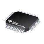
| 描述 | IC RGBHV VIDEO BUFFR 3CH 48HTQFP视频放大器 3-Ch RGBHV Video Buffer |
| 产品分类 | |
| 品牌 | Texas Instruments |
| 产品手册 | http://www.ti.com/lit/gpn/ths7347 |
| 产品图片 |
|
| rohs | 符合RoHS无铅 / 符合限制有害物质指令(RoHS)规范要求 |
| 产品系列 | 放大器 IC,视频放大器,Texas Instruments THS7347IPHP- |
| 数据手册 | |
| 产品型号 | THS7347IPHP |
| PCN组件/产地 | |
| PCN设计/规格 | |
| 产品 | Video Amplifiers |
| 产品目录页面 | |
| 产品种类 | 视频放大器 |
| 供应商器件封装 | 48-HTQFP(7x7) |
| 其它名称 | 296-21966-5 |
| 包装 | 托盘 |
| 单位重量 | 134.500 mg |
| 压摆率 | 1200 V/µs |
| 商标 | Texas Instruments |
| 安装类型 | 表面贴装 |
| 安装风格 | SMD/SMT |
| 封装 | Tray |
| 封装/外壳 | 48-TQFP 裸露焊盘 |
| 封装/箱体 | HTQFP-48 |
| 工作温度范围 | - 40 C to + 85 C |
| 工作电源电压 | 2.7 V to 5.5 V |
| 工厂包装数量 | 250 |
| 应用 | 缓冲器 |
| 最大工作温度 | + 85 C |
| 最小工作温度 | - 40 C |
| 标准包装 | 250 |
| 电压-电源,单/双 (±) | 2.7 V ~ 5.5 V |
| 电流-电源 | 90mA |
| 电流-输出/通道 | 110mA |
| 电源电压-最大 | 5.5 V |
| 电源电压-最小 | 2.7 V |
| 电源电流 | 80 mA |
| 电源类型 | Single |
| 电路数 | 3 |
| 系列 | THS7347 |
| 输出类型 | 满摆幅 |
| 通道数量 | 3 Channel |
| 配用 | /product-detail/zh/THS7347EVM/THS7347EVM-ND/1905377 |


- 商务部:美国ITC正式对集成电路等产品启动337调查
- 曝三星4nm工艺存在良率问题 高通将骁龙8 Gen1或转产台积电
- 太阳诱电将投资9.5亿元在常州建新厂生产MLCC 预计2023年完工
- 英特尔发布欧洲新工厂建设计划 深化IDM 2.0 战略
- 台积电先进制程称霸业界 有大客户加持明年业绩稳了
- 达到5530亿美元!SIA预计今年全球半导体销售额将创下新高
- 英特尔拟将自动驾驶子公司Mobileye上市 估值或超500亿美元
- 三星加码芯片和SET,合并消费电子和移动部门,撤换高东真等 CEO
- 三星电子宣布重大人事变动 还合并消费电子和移动部门
- 海关总署:前11个月进口集成电路产品价值2.52万亿元 增长14.8%


PDF Datasheet 数据手册内容提取
THS7347 www.ti.com SLOS531B–MAY2007–REVISEDOCTOBER2011 2 3-Channel RGBHV Video Buffer with I C™ Control, 2:1 Input Mux, Monitor Pass-Through, and Selectable Input Bias Modes CheckforSamples:THS7347 FEATURES APPLICATIONS 1 • 3-VideoAmplifiersforCVBS,S-Video,EDTV, • Projectors 2345 HDTVY'P'BP'R,G'B'R',andR'G'B'Video • ProfessionalVideoSystems • H/VSyncPathswithAdjustableSchmitt • LCD/DLP®/LOCSInputBuffering Trigger • 2:1InputMux DESCRIPTION • I2CControlofAllFunctionsonEachChannel Fabricated using the revolutionary complimentary silicon-germanium (SiGe) BiCom3 process, the • Unity-GainBufferPathforADCBuffering: THS7347 is a low-power, single-supply 2.7-V to 5-V – 500-MHzBandwidth,1200-V/μsSlewRate 3-channel integrated video buffer with horizontal (H) • MonitorPass-ThroughFunction: and vertical (V) sync signal paths. It incorporates a 500-MHzbandwidth,1200-V/μsunity-gainbufferideal – 500-MHzBandwidth,1300-V/μsSlewRate for driving analog-to-digital converters (ADCs) and – 6-dBGainwithSAGCorrectionCapable video decoders. In parallel with the unity-gain buffer, – HighOutputImpedanceinDisableState a monitor pass-through path allows for passing the • SelectableInputBiasModes: input signal on to other systems. This path has a 6-dB gain, 500-MHz bandwidth, 1300-V/μs slew rate, – AC-CoupledwithSync-TipClamp SAGcorrectioncapability,andhighoutputimpedance – AC-CoupledwithBias whiledisabled. – DC-CoupledwithOffsetShift Each channel of the THS7347 is individually – DC-Coupled I2C-configurable for all functions, including controlling • +2.7-Vto+5-VSingle-SupplyOperation the 2:1 input mux. Its rail-to-rail output stage allows forbothac-anddc-couplingapplications. • TotalPowerConsumption:265mWat3.3V • DisableFunctionReducesCurrentto0.1μA • Rail-to-RailOutput: – OutputSwingsWithin0.1VoftheRails, AllowingAC-orDC-OutputCoupling • Lead-free,RoHSTQFPPackage 3.3 V Input 1 0.1mF InA In B 2:1 X1 + 0.1mF 75W ADC - AC Input 2 0.1mF +ODffCset DC STyInPc + 47mF Clamp Out AC- 75W BIAS D=iOsaPbElNe - 675W 33mF 75W SAG Monitor 1 kW 878W 150W Output 75W SDA SCL 3.3 V 3.3VSingle-SupplyProjectorInputSystemwithMonitorPass-Through (OneofThreeR'G'B' ChannelsShown) 1 Pleasebeawarethatanimportantnoticeconcerningavailability,standardwarranty,anduseincriticalapplicationsofTexas Instrumentssemiconductorproductsanddisclaimerstheretoappearsattheendofthisdatasheet. PowerPADisatrademarkofTexasInstruments. 2 DLPisaregisteredtrademarkofTexasInstruments. 3I2CisatrademarkofNXPSemiconductors,Inc. 4 Allothertrademarksarethepropertyoftheirrespectiveowners. 5 PRODUCTIONDATAinformationiscurrentasofpublicationdate. Copyright©2007–2011,TexasInstrumentsIncorporated Products conform to specifications per the terms of the Texas Instruments standard warranty. Production processing does not necessarilyincludetestingofallparameters.
THS7347 SLOS531B–MAY2007–REVISEDOCTOBER2011 www.ti.com DESCRIPTION, CONTINUED As part of the THS7347 flexibility, the device input can be selected for ac- or dc-coupled inputs. The ac-coupled modes include a sync-tip clamp option for CVBS/Y'/G'B'R' with sync or a fixed bias for the C'/P' /P' /R'G'B' B R channels without sync. The dc input options include a dc input or a dc+Offset shift to allow for a full sync dynamicrangeattheoutputwith0-Vinput. TheTHS7347isavailableinalead-free,RoHS-compliantTQFPpackage. This integrated circuit can be damaged by ESD. Texas Instruments recommends that all integrated circuits be handled with appropriateprecautions.Failuretoobserveproperhandlingandinstallationprocedurescancausedamage. ESDdamagecanrangefromsubtleperformancedegradationtocompletedevicefailure.Precisionintegratedcircuitsmaybemore susceptibletodamagebecauseverysmallparametricchangescouldcausethedevicenottomeetitspublishedspecifications. PACKAGING/ORDERINGINFORMATION(1) PACKAGEDDEVICES PACKAGETYPE TRANSPORTMEDIA,QUANTITY THS7347IPHP Tray,250 HTQFP-48PowerPAD™ THS7347IPHPR TapeandReel,1000 (1) Forthemostcurrentpackageandorderinginformation,seethePackageOptionAddendumattheendofthisdocument,orseetheTI websiteatwww.ti.com. ABSOLUTE MAXIMUM RATINGS(1) Overoperatingfree-airtemperaturerange(unlessotherwisenoted). THS7347 UNIT V Supplyvoltage,GNDtoV orGNDtoV 5.5 V SS A DD V Inputvoltage –0.4toV orV V I A DD I Continuousoutputcurrent ±80 mA O Continuouspowerdissipation SeeDissipationRatingTable T Maximumjunctiontemperature,anycondition(2) +150 °C J T Maximumjunctiontemperature,continuousoperation,longtermreliability(3) +125 °C J T Storagetemperaturerange –65to+150 °C stg Leadtemperature1,6mm(1/16inch)fromcasefor10seconds 300 °C HBM 1500 V ESDratings CDM 1500 V MM 100 V (1) Stressesabovethoselistedunderabsolutemaximumratingsmaycausepermanentdamagetothedevice.Thesearestressratings only,andfunctionaloperationofthedeviceattheseoranyotherconditionsbeyondthoseindicatedunderrecommendedoperating conditionsisnotimpliedExposuretoabsolutemaximumratedconditionsforextendedperiodsmaydegradedevicereliability. (2) Theabsolutemaximumjunctiontemperatureunderanyconditionislimitedbytheconstraintsofthesiliconprocess. (3) Theabsolutemaximumjunctiontemperatureforcontinuousoperationislimitedbythepackageconstraints.Operationabovethis temperaturemayresultinreducedreliabilityand/orlifetimeofthedevice. DISSIPATION RATINGS POWERRATING(1)(2) (T =+125°C) θ θ J JC JA PACKAGE (°C/W) (°C/W) T =+25°C T =+85°C A A HTQFP-48withPowerPAD(PHP) 1.2 35 2.85W 1.14W (1) ThisdatawastakenwithaPowerPADstandard3-inchby3-inch,4-layerprintedcircuitboard(PCB)withinternalgroundplane connectionstothePowerPAD. (2) Powerratingisdeterminedwithajunctiontemperatureof+125°C.Thistemperatureisthepointwheredistortionstartstosubstantially increaseandlong-termreliabilitystartstobereduced.ThermalmanagementofthefinalPCBshouldstrivetokeepthejunction temperatureatorbelow+125°Cforbestperformanceandreliability. 2 Copyright©2007–2011,TexasInstrumentsIncorporated
THS7347 www.ti.com SLOS531B–MAY2007–REVISEDOCTOBER2011 RECOMMENDED OPERATING CONDITIONS MIN NOM MAX UNIT V Digitalsupplyvoltage 2.7 5 V DD V Analogsupplyvoltage.MustbeequaltoorgreaterthanV V 5 V A DD DD T Ambienttemperature –40 +85 °C A ELECTRICAL CHARACTERISTICS, V = V = 3.3 V A DD R =150Ω∥5pFtoGNDforMonitorOutput,19kΩ||8pFLoadtoGNDforBufferOutput,SAGpinshortedtoMonitor L OutputPin,unlessotherwisenoted. TYP OVERTEMPERATURE 0°Cto –40°Cto MIN/MAX/ PARAMETER TESTCONDITIONS +25°C +25°C +70°C +85°C UNIT TYP ACPERFORMANCE Small-signal Bufferoutput 500 MHz Typ bandwidth(–3dB) Monitoroutput VO=0.2VPP 450 MHz Typ Bufferoutput 425 MHz Typ –1dBflatness VO=0.2VPP Monitoroutput 375 MHz Typ Large-signal Bufferoutput VO=1VPP 475 MHz Typ bandwidth(–3dB) Monitoroutput VO=2VPP 240 MHz Typ Bufferoutput VO=1VPP 1050 V/μs Typ Slewrate Monitoroutput VO=2VPP 1050 V/μs Typ Groupdelayat Bufferoutput 1.2 ns Typ 100kHz Monitoroutput 1.2 ns Typ Bufferoutput 0.05/0.05 % Typ Differentialgain NTSC/PAL Monitoroutput 0.1/0.1 % Typ Bufferoutput 0.1/0.15 degrees Typ Differentialphase NTSC/PAL Monitoroutput 0.15/0.2 degrees Typ Totalharmonic Bufferoutput VO=1VPP –58 dB Typ distortionf=1MHz Monitoroutput VO=2VPP –57 dB Typ Bufferoutput 63 dB Typ Signal-to-noiseratio Noweighting,upto100MHz Monitoroutput 65 dB Typ Channel-to-channel Bufferoutput –40 dB Typ f=100MHz crosstalk Monitoroutput –36 dB Typ Bufferoutput 64 dB Typ MUXisolation f=100MHz Monitoroutput 66 dB Typ Bufferoutput f=100kHz;VO=1VPP 0 dB Typ Gain Monitoroutput f=100kHz;VO=2VPP 6 5.8/6.25 5.75/6.3 5.75/6.35 dB Min/Max Bufferoutput 6 ns Typ Settlingtime VIN=1VPP;0.5%settling Monitoroutput 6 ns Typ Bufferoutput 0.3 Ω Typ Outputimpedance f=10MHz Monitoroutput 0.4 Ω Typ DCPERFORMANCE Bufferoutput 15 ±80 ±85 ±85 mV Max Outputoffsetvoltage Bias=dc Monitoroutput 20 ±120 ±125 ±125 mV Max Averageoffset Bufferoutput 20 μV/°C Typ Bias=dc voltagedrift Monitoroutput 20 μV/°C Typ Bias=dc+shift,VIN=0V 255 175/355 165/365 160/370 mV Min/Max Bufferoutput Bias=ac 1.0 0.85/1.15 0.8/1.2 0.8/1.2 V Min/Max Biasoutputvoltage Bias=dc+shift,VIN=0V 235 145/350 135/360 130/365 mV Min/Max Monitoroutput Bias=ac 1.7 1.55/1.85 1.5/1.9 1.5/1.9 V Min/Max Synctipclamp Bufferoutput 290 200/405 195/410 190/415 mV Min/Max Bias=acSTC,clampvoltage voltage Monitoroutput 300 200/400 195/405 190/410 mV Min/Max Copyright©2007–2011,TexasInstrumentsIncorporated 3
THS7347 SLOS531B–MAY2007–REVISEDOCTOBER2011 www.ti.com ELECTRICAL CHARACTERISTICS, V = V = 3.3 V (continued) A DD R =150Ω∥5pFtoGNDforMonitorOutput,19kΩ||8pFLoadtoGNDforBufferOutput,SAGpinshortedtoMonitor L OutputPin,unlessotherwisenoted. TYP OVERTEMPERATURE 0°Cto –40°Cto MIN/MAX/ PARAMETER TESTCONDITIONS +25°C +25°C +70°C +85°C UNIT TYP DCPERFORMANCE,continued Inputbiascurrent Bias=dc;(–)impliesIBoutofthepin –1.3 –3.0 –3.5 –3.5 μA Max Averagebiascurrentdrift Bias=dc 10 nA/°C Typ Bias=acSTC,lowbias 2.3 0.9/3.6 0.8/3.8 0.7/3.9 μA Min/Max Synctipclampbiascurrent Bias=acSTC,midbias 5.8 3.8/8.0 3.7/8.2 3.6/8.3 μA Min/Max Bias=acSTC,highbias 8.1 5.7/10.8 5.6/11.0 5.5/11.1 μA Min/Max INPUTCHARACTERISTICS Inputvoltagerange Bias=dc 0to2 V Typ Bias=acbiasmode 25 kΩ Typ Inputresistance Bias=dc,dc+shift,acSTC 3 MΩ Typ Inputcapacitance 1.5 pF Typ OUTPUTCHARACTERISTICS:MONITOROUTPUT RL=150Ωto1.65V 3.15 2.9 2.8 2.8 V Min RL=150ΩtoGND 3.05 2.85 2.75 2.75 V Min Highoutputvoltageswing RL=75Ωto1.65V 3.05 V Typ RL=75ΩtoGND 2.9 V Typ RL=150Ωto1.65V 0.15 0.25 0.28 0.29 V Max RL=150ΩtoGND 0.1 0.18 0.21 0.22 V Max Lowoutputvoltageswing RL=75Ωto1.65V 0.25 V Typ RL=75ΩtoGND 0.08 V Typ Sourcing 80 50 47 45 mA Min Outputcurrent RL=10Ωto1.65V Sinking 75 50 47 45 mA Min OUTPUTCHARACTERISTICS:BUFFEROUTPUT Highoutputvoltageswing 2 1.8 1.75 1.75 V Min (LimitedbyinputrangeandG=0dB) Load=19kΩ∥8pFto1.65V LowOutputvoltageswing 0.05 0.12 0.13 0.14 V Max (LimitedbyinputrangeandG=0dB) Sourcing RL=10ΩtoGND 80 50 47 45 mA Min OutputCurrent Sinking RL=10Ωto1.65V 75 50 47 45 mA Min POWERSUPPLY:ANALOG Maximumoperatingvoltage VA 3.3 5.5 5.5 5.5 V Max Minimumoperatingvoltage VA 3.3 2.7 2.7 2.7 V Min Maximumquiescentcurrent VA,dc+shiftmode,VIN=100mV 80 100 103 105 mA Max Minimumquiescentcurrent VA,dc+shiftmode,VIN=100mV 80 60 57 55 mA Min Powersupplyrejection(+PSRR) Bufferoutput 50 dB Typ POWERSUPPLY:DIGITAL Maximumoperatingvoltage VDD 3.3 5.5 5.5 5.5 V Max Minimumoperatingvoltage VDD 3.3 2.7 2.7 2.7 V Min Maximumquiescentcurrent VDD,VIN=0V 0.65 1.2 1.3 1.4 mA Max Minimumquiescentcurrent VDD,VIN=0V 0.65 0.35 0.3 0.25 mA Min DISABLECHARACTERISTICS:ALLCHANNELSDISABLED Quiescentcurrent Allchannelsdisabled 0.1 μA Typ Turn-ontimedelay(tON) TimeforlStoreach50%offinalvalue 5 μs Typ Turn-ontimedelay(tOFF) afterI2Ccontrolisinitiated 2 μs Typ 4 Copyright©2007–2011,TexasInstrumentsIncorporated
THS7347 www.ti.com SLOS531B–MAY2007–REVISEDOCTOBER2011 ELECTRICAL CHARACTERISTICS, V = V = 3.3 V (continued) A DD R =150Ω∥5pFtoGNDforMonitorOutput,19kΩ||8pFLoadtoGNDforBufferOutput,SAGpinshortedtoMonitor L OutputPin,unlessotherwisenoted. TYP OVERTEMPERATURE 0°Cto –40°Cto MIN/MAX/ PARAMETER TESTCONDITIONS +25°C +25°C +70°C +85°C UNIT TYP DIGITALCHARACTERISTICS(1) Highlevelinputvoltage VIH 2.3 V Typ Lowlevelinputvoltage VIL 1.0 V Typ H/VSYNCCHARACTERISTICS:RLoad=1kΩToGND(2) Schmitttriggeradjustpinvoltage ReferenceforSchmitttrigger 1.47 1.35/1.6 1.3/1.65 1.27/1.68 V Min/Max Schmitttriggerthresholdrange AllowablerangeforSchmitttriggeradjust 0.9to2 V Typ Positive-goinginputvoltagethreshold SchmitttriggerVT+ 0.25 V Typ relativetoSchmitttriggerthreshold Negative-goinginputvoltagethreshold SchmitttriggerVT– –0.3 V Typ relativetoSchmitttriggerthreshold Schmitttriggerthresholdpininput InputresistanceintoControlpin 10 kΩ Typ resistance H/VSyncinputimpedance 10 MΩ Typ H/VSynchighoutputvoltage 1kΩtoGND 3.15 3.05 3.0 3.0 V Min H/VSynclowoutputvoltage 1kΩtoGND 0.01 0.05 0.1 0.1 V Max H/VSyncsourcecurrent 10ΩtoGND 50 35 30 30 mA Min H/VSyncsinkcurrent 10Ωto3.3V 35 25 23 21 mA Min H/VDelay DelayfromInputtooutput 6.5 ns Typ H/Vtobufferoutputskew 5 ns Typ (1) StandardCMOSlogic. (2) Schmitttriggerthresholdisdefinedby(VT+–VT–)/2. Copyright©2007–2011,TexasInstrumentsIncorporated 5
THS7347 SLOS531B–MAY2007–REVISEDOCTOBER2011 www.ti.com ELECTRICAL CHARACTERISTICS, V = V = 5 V A DD R =150Ω||5pFtoGNDforMonitorOutput,19kΩ||8pFLoadtoGNDforBufferOutput,SAGpinshortedtoMonitorOutput L Pin,unlessotherwisenoted. TYP OVERTEMPERATURE 0°Cto –40°Cto MIN/MAX/ PARAMETER TESTCONDITIONS +25°C +25°C +70°C +85°C UNIT TYP ACPERFORMANCE Small-signal Bufferoutput 550 MHz Typ bandwidth(–3dB) Monitoroutput VO=0.2VPP 500 MHz Typ Bufferoutput 450 MHz Typ –1dBflatness VO=0.2VPP Monitoroutput 400 MHz Typ Large-signal Bufferoutput VO=1VPP 525 MHz Typ bandwidth(–3dB) Monitoroutput VO=2VPP 325 MHz Typ Bufferoutput VO=1VPP 1200 V/μs Typ Slewrate Monitoroutput VO=2VPP 1350 V/μs Typ Groupdelayat Bufferoutput 1.15 ns Typ 100kHz Monitoroutput 1.15 ns Typ Bufferoutput 0.05/0.05 % Typ Differentialgain NTSC/PAL Monitoroutput 0.1/0.1 % Typ Bufferoutput 0.05/0.05 degrees Typ Differentialphase NTSC/PAL Monitoroutput 0.05/0.05 degrees Typ Totalharmonic Bufferoutput VO=1VPP –71 dB Typ distortionf=1MHz Monitoroutput VO=2VPP –67 dB Typ Bufferoutput 63 dB Typ Signal-to-noiseratio Noweighting,upto100MHz Monitoroutput 65 dB Typ Channel-to-channel Bufferoutput –40 dB Typ f=100MHz crosstalk Monitoroutput –36 dB Typ Bufferoutput 64 dB Typ MUXIsolation f=100MHz Monitoroutput 66 dB Typ Bufferoutput f=100kHz;VO=1VPP 0 dB Typ Gain Monitoroutput f=100kHz;VO=2VPP 6 5.8/6.25 5.75/6.3 5.75/6.35 dB Min/Max Bufferoutput 6 ns Typ Settlingtime VIN=1VPP;0.5%settling Monitoroutput 6 ns Typ Bufferoutput 0.3 Ω Typ Outputimpedance f=10MHz Monitoroutput 0.4 Ω Typ DCPERFORMANCE Bufferoutput 15 ±80 ±85 ±85 mV Max Outputoffsetvoltage Bias=dc Monitoroutput 20 ±120 ±125 ±125 mV Max Averageoffset Bufferoutput 20 μV/°C Typ Bias=dc voltagedrift Monitoroutput 20 μV/°C Typ Bias=dc+shift,VIN=0V 265 185/370 175/380 170/385 mV Min/Max Bufferoutput Bias=ac 1.5 1.3/1.65 1.25/1.7 1.25/1.7 V Min/Max Biasoutputvoltage Bias=dc+shift,VIN=0V 235 145/345 135/355 130/360 mV Min/Max Monitoroutput Bias=ac 2.65 2.5/2.8 2.45/2.85 2.45/2.85 V Min/Max Synctipclamp Bufferoutput 295 205/410 200/415 195/420 mV Min/Max Bias=acSTC,clampvoltage voltage Monitoroutput 300 200/400 195/405 190/410 mV Min/Max Inputbiascurrent Bias=dc;(–)impliesIBoutofthepin –1.4 –3.0 –3.5 –3.5 μA Max Averagebiascurrentdrift Bias=dc 10 nA/°C Typ Bias=acSTC,lowbias 2.4 0.9/3.9 0.8/4.0 0.7/4.1 μA Min/Max Synctipclampbiascurrent Bias=acSTC,midbias 6.2 3.9/8.4 3.8/8.6 3.7/8.7 μA Min/Max Bias=acSTC,highbias 8.6 6/11.2 5.8/11.4 5.7/11.5 μA Min/Max 6 Copyright©2007–2011,TexasInstrumentsIncorporated
THS7347 www.ti.com SLOS531B–MAY2007–REVISEDOCTOBER2011 ELECTRICAL CHARACTERISTICS, V = V = 5 V (continued) A DD R =150Ω||5pFtoGNDforMonitorOutput,19kΩ||8pFLoadtoGNDforBufferOutput,SAGpinshortedtoMonitorOutput L Pin,unlessotherwisenoted. TYP OVERTEMPERATURE 0°Cto –40°Cto MIN/MAX/ PARAMETER TESTCONDITIONS +25°C +25°C +70°C +85°C UNIT TYP INPUTCHARACTERISTICS Inputvoltagerange Bias=dc 0to3.4 V Typ Bias=acbiasmode 25 kΩ Typ Inputresistance Bias=dc,dc+shift,acSTC 3 MΩ Typ Inputcapacitance 1.5 pF Typ OUTPUTCHARACTERISTICS:MONITOROUTPUT RL=150Ωto2.5V 4.8 4.65 4.6 4.6 V Min RL=150ΩtoGND 4.7 4.55 4.5 4.5 V Min Highoutputvoltageswing RL=75Ωto2.5V 4.7 V Typ RL=75ΩtoGND 4.6 V Typ RL=150Ωto2.5V 0.2 0.25 0.28 0.30 V Max RL=150ΩtoGND 0.1 0.19 0.23 0.24 V Max Lowoutputvoltageswing RL=75Ωto2.5V 0.24 V Typ RL=75ΩtoGND 0.085 V Typ Sourcing 110 85 80 75 mA Min Outputcurrent RL=10Ωto2.5V Sinking 110 85 80 75 mA Min OUTPUTCHARACTERISTICS:BUFFEROUTPUT Highoutputvoltageswing 3.4 3.1 3.0 3.0 V Min (LimitedbyinputrangeandG=0dB) Load=19kΩ∥8pFto2.5V Lowoutputvoltageswing 0.05 0.12 0.13 0.14 V Max (LimitedbyinputrangeandG=0dB) Sourcing RL=10ΩtoGND 110 85 80 75 mA Min Outputcurrent Sinking RL=10Ωto2.5V 110 85 80 75 mA Min POWERSUPPLY:ANALOG Maximumoperatingvoltage VA 5.0 5.5 5.5 5.5 V Max Minimumoperatingvoltage VA 5.0 2.7 2.7 2.7 V Min Maximumquiescentcurrent VA,dc+shiftmode,VIN=100mV 90 112 115 117 mA Max Minimumquiescentcurrent VA,dc+shiftmode,VIN=100mV 90 68 65 63 mA Min Powersupplyrejection(+PSRR) BufferOutput 46 dB Typ POWERSUPPLY:DIGITAL Maximumoperatingvoltage VDD 5.0 5.5 5.5 5.5 V Max Minimumoperatingvoltage VDD 5.0 2.7 2.7 2.7 V Min Maximumquiescentcurrent VDD,VIN=0V 1 2 3 3 mA Max Minimumquiescentcurrent VDD,VIN=0V 1 0.5 0.4 0.4 mA Min DIGITALCHARACTERISTICS(1) Highlevelinputvoltage VIH 3.5 V Typ Lowlevelinputvoltage VIL 1.5 V Typ DISABLECHARACTERISTICS:ALLCHANNELSDISABLED Quiescentcurrent Allchannelsdisabled 1 μA Typ Turn-ontimedelay(tON) TimeforlStoreach50%offinalvalue 5 μs Typ Turn-ontimedelay(tOFF) afterI2Ccontrolisinitiated 2 μs Typ (1) StandardCMOSlogic. Copyright©2007–2011,TexasInstrumentsIncorporated 7
THS7347 SLOS531B–MAY2007–REVISEDOCTOBER2011 www.ti.com ELECTRICAL CHARACTERISTICS, V = V = 5 V (continued) A DD R =150Ω||5pFtoGNDforMonitorOutput,19kΩ||8pFLoadtoGNDforBufferOutput,SAGpinshortedtoMonitorOutput L Pin,unlessotherwisenoted. TYP OVERTEMPERATURE 0°Cto –40°Cto MIN/MAX/ PARAMETER TESTCONDITIONS +25°C +25°C +70°C +85°C UNIT TYP H/VSYNCCHARACTERISTICS:RLoad=1kΩToGND(2) Schmitttriggeradjustpinvoltage ReferenceforSchmitttrigger 1.54 1.43/1.65 1.38/1.7 1.35/1.73 V Min/Max Schmitttriggerthresholdrange AllowablerangeforSchmitttriggeradjust 0.9to2 V Typ Positive-goinginputvoltagethreshold SchmitttriggerVT+ 0.25 V Typ relativetoSchmitttriggerthreshold Negative-goinginputvoltagethreshold SchmitttriggerVT– –0.3 V Typ relativetoSchmitttriggerthreshold Schmitttriggerthresholdpininput InputresistanceintoControlpin 10 kΩ Typ resistance H/VSyncinputimpedance 10 MΩ Typ H/VSynchighoutputvoltage 1kΩtoGND 4.8 4.7 4.6 4.6 V Min H/VSynclowoutputvoltage 1kΩtoGND 0.01 0.05 0.1 0.1 V Max H/VSyncsourcecurrent 10ΩtoGND 90 60 55 55 mA Min H/VSyncsinkcurrent 10Ωto5V 50 30 27 25 mA Min H/VDelay Delayfrominputtooutput 6.5 ns Typ H/Vtobufferoutputskew 5 ns Typ (2) Schmitttriggerthresholdisdefinedby(VT+–VT–)/2. 8 Copyright©2007–2011,TexasInstrumentsIncorporated
THS7347 www.ti.com SLOS531B–MAY2007–REVISEDOCTOBER2011 TIMING REQUIREMENTS FOR I2C INTERFACE(1)(2) AtV =2.7Vto5V. DD STANDARDMODE FASTMODE PARAMETER MIN MAX MIN MAX UNIT f Clockfrequency,SCL 0 100 0 400 kHz SCL t Pulseduration,SCLhigh 4 0.6 μs w(H) t Pulseduration,SCLlow 4.7 1.3 μs w(L) t Risetime,SCLandSDA 1000 300 ns r t Falltime,SCLandSDA 300 300 ns f t Setuptime,SDAtoSCL 250 100 ns su(1) t Holdtime,SCLtoSDA 0 0 ns h(1) t Busfreetimebetweenstopandstartconditions 4.7 1.3 μs (buf) t Setuptime,SCLtostartcondition 4.7 0.6 μs su(2) t Holdtime,startconditiontoSCL 4 0.6 μs h(2) t Setuptime,SCLtostopcondition 4 0.6 μs su(3) C Capacitiveloadforeachbusline 400 400 pF b (1) TheTHS7347I2Caddress=01011(A1)(A0)(R/W).SeetheApplicationsInformationsectionformoreinformation. (2) TheTHS7347wasdesignedtocomplywithversion2.1oftheI2Cspecification. tw(H) tw(L) tr tf SCL tsu(1) th(1) SDA Figure1. SCLandSDATiming SCL tsu(2) th(2) tsu(3) t(buf) SDA Start Condition Stop Condition Figure2. StartandStopConditions Copyright©2007–2011,TexasInstrumentsIncorporated 9
THS7347 SLOS531B–MAY2007–REVISEDOCTOBER2011 www.ti.com FUNCTIONAL BLOCK DIAGRAM Channel 1 Input A 2:1 X1 + Channel 2 - Channel 1 Buffer Input A AC Output (To ADC) Channel 3 DC Sync Input A +Offset DC TIP Clamp + H-Sync AC- Channel 1 Monitor Input A BIAS Disable - Output = OPEN 675W V-Sync Input A Channel 1 SAG 1 kW 878W 150W 2:1 X1 + Channel 2 Buffer - AC Output (To ADC) DC Sync +Offset DC TIP + Clamp AC- Channel 2 Monitor BIAS Disable - Output = OPEN 675W Channel 2 SAG 1 kW 878W 150W 2:1 X1 + Channel 3 Buffer - AC Output (To ADC) DC Sync +Offset DC TIP Clamp + AC- Channel 3 Monitor BIAS Disable - Output = OPEN 675W Channel 3 SAG 1 kW 878W 150W Channel 1 Input B 2:1 + Horizontal Sync Channel 2 Buffer OUTPUT - Input B Channel 3 Input B Horizontal Sync Monitor OUTPUT H-Sync Input B V-Sync 2:1 + VerticalSync Input B - Buffer OUTPUT 10 kW VerticalSync +1.4 V Monitor OUTPUT MUX MUX SCHMITT SDA SCL I2C, I2C, PUC MODE SELECT TARDIGJUGSETR A1 A0 +VDD DGND +VA AGND NOTE: TheI2CaddressoftheTHS7347is01011(A1)(A0)(R/W). 10 Copyright©2007–2011,TexasInstrumentsIncorporated
THS7347 www.ti.com SLOS531B–MAY2007–REVISEDOCTOBER2011 PIN CONFIGURATION THS7347IPHP HTQFP-48(PHP) (TopView) T T T R OUTPU R OUTPU R OUTPU OUTPUT OUTPUT TO TO TO N. N. MONI SAG MONI SAG MONI SAG C MO C MO +VA AGND CH. 1, CH. 1, CH. 2, CH. 2, CH. 3, CH. 3, H-SYN V-SYN +VA AGND 48 47 46 45 44 43 42 41 40 39 38 37 CH. 1, INPUT A 1 36 CH. 1, BUFFER OUTPUT CH. 2, INPUT A 2 35 CH. 1, BUFFER OUTPUT CH. 3, INPUT A 3 34 AGND H-SYNC, INPUT A 4 33 +VA V-SYNC, INPUT A 5 32 CH. 2, BUFFER OUTPUT AGND 6 THS7347 31 CH. 2, BUFFER OUTPUT PowerPAD CH. 1, INPUT B 7 30 AGND CH. 2, INPUT B 8 29 +VA CH. 3, INPUT B 9 28 CH. 3, BUFFER OUTPUT H-SYNC, INPUT B 10 27 CH. 3, BUFFER OUTPUT V-SYNC, INPUT B 11 26 AGND AGND 12 25 H-SYNC BUFFER OUTPUT 3 4 5 6 7 8 9 0 1 2 3 4 1 1 1 1 1 1 1 2 2 2 2 2 ND DJ. DE CT A1 A0 DA CL UC DD ND UT AG ER A X MO SELE I2C, I2C, S S P V DG OUTP RIGG MU MUX FER T F T- U T B MI C H N C Y S S V- TERMINALFUNCTIONS TERMINAL I/O DESCRIPTION NAME NO. CH.1,INPUTA 1 I VideoInputChannel1,InputA CH.2,INPUTA 2 I VideoInputChannel2,InputA CH.3,INPUTA 3 I VideoInputChannel3,InputA H-SYNC,INPUTA 4 I HorizontalSync,InputA V-SYNC,INPUTA 5 I VerticalSync,InputA CH.1,INPUTB 7 I VideoInputChannel1,InputB CH.2,INPUTB 8 I VideoInputChannel2,InputB CH.3,INPUTB 9 I VideoInputChannel3,InputB Copyright©2007–2011,TexasInstrumentsIncorporated 11
THS7347 SLOS531B–MAY2007–REVISEDOCTOBER2011 www.ti.com TERMINALFUNCTIONS(continued) TERMINAL I/O DESCRIPTION NAME NO. H-SYNC,INPUTB 10 I HorizontalSync,InputB V-SYNC,INPUTB 11 I VerticalSync,InputB I2C,A1 17 I I2CSlaveAddressControlBitA1.ConnecttoVDDforalogic1presetvalueorGNDforalogic0preset value. I2C,A0 18 I I2CSlaveAddressControlBitA0.ConnecttoVDDforalogic1presetvalueorGNDforalogic0preset value. SerialdatalineoftheI2Cbus.Pull-upresistorshouldhaveaminimumvalue=2kΩandamaximumvalue SDA 19 I/O =19kΩ.PulluptoVDD. I2Cbusclockline.Pull-upresistorshouldhaveaminimumvalue=2kΩandamaximumvalue=19-kΩ. SCL 20 I PulluptoVDD. Power-UpCondition.ConnecttoGNDforallchannelsdisableduponpower-up.ConnecttoVDD(logic PUC 21 I high)tosetbufferoutputstoOFFandmonitoroutputsONwithac-biasconfigurationonChannels1to3 andbothH-Sync/V-Syncenabled. SetstheMUXconfigurationcontrol.ConnecttologiclowforMUXSelect(pin16)controloftheMUX. MUXMODE 15 I ConnecttologichighforI2CcontroloftheMUX. ControlstheMUXselectionwhenMUXMODE(pin15)issettologiclow.ConnecttologiclowforMUX MUXSELECT 16 I selectorsettoInputA.ConnecttologichighforMUXselectorsettoInputB. OutputChannel1fromeitherCH.1,INPUTAorCH.1,INPUTB.ConnecttoADC/Scalar/Decoder.Both CH.1,BUFFEROUTPUT 35,36 O pinsshouldbeconnectedtogetheronthePCB. OutputChannel2fromeitherCH.2,INPUTAorCH.2,INPUTB.ConnecttoADC/Scalar/Decoder.Both CH.2,BUFFEROUTPUT 31,32 O pinsshouldbeconnectedtogetheronthePCB. OutputChannel3fromeitherCH.3,INPUTAorCH.3,INPUTB.ConnecttoADC/Scalar/Decoder.Both CH.3,BUFFEROUTPUT 27,28 O pinsshouldbeconnectedtogetheronthePCB. H-SYNCBUFFER 25 O HorizontalSyncBufferOutput.ConnecttoADC/ScalarH-syncinput. OUTPUT V-SYNCBUFFER 24 O VerticalSyncBufferOutput.ConnecttoADC/ScalarV-syncinput. OUTPUT VideoMonitorPass-ThroughOutputChannel1SAGCorrectionpin.IfSAGisnotused,connectDirectlyto CH.1,SAG 45 O CH.1,OUTPUTpin46. CH.1,MONITOR 46 O VideoMonitorPass-ThroughOutputChannel1fromeitherCH.1,INPUTAorCH.1,INPUTB. OUTPUT VideoMonitorPass-ThroughOutputChannel2SAGCorrectionpin.IfSAGisnotused,connectDirectlyto CH.2,SAG 43 O CH.2,OUTPUTpin44. CH.2,MONITOR 44 O VideoMonitorPass-ThroughOutputChannel2fromeitherCH.2,INPUTAorCH.2,INPUTB. OUTPUT VideoMonitorPass-ThroughOutputChannel3SAGCorrectionpin.IfSAGisnotused,connectDirectlyto CH.3,SAG 41 O CH.3,OUTPUTpin42. CH.3,MONITOR 42 O VideoMonitorPass-ThroughOutputChannel3fromeitherCH.3,INPUTAorCH.3,INPUTB. OUTPUT H-SYNCMONITOR 40 O HorizontalSyncMonitorPass-ThroughOutput. OUTPUT V-SYNCMONITOR 39 O VerticalSyncMonitorPass-ThroughOutput. OUTPUT 6,12,13,26, GroundReferencepinforanalogsignals.Internally,thesepinsconnecttoDGND,althoughitis AGND I 30,34,37,47 recommendedtohavetheAGNDandDGNDconnectedtothepropersignalsforbestresults. +VA 29,33,38,48 I AnalogPositivePowerSupplyInputpins.Connectto2.7Vto5V.MustbeequaltoorgreaterthanVDD. VDD 22 I DigitalPositiveSupplypinforI2CcircuitryandH-Sync/V-Syncoutputs.Connectto2.7Vto5V. DGND 23 I DigitalGNDpinforHVcircuitryandI2Ccircuitry. Defaultsto1.45V(TTLcompatible).ConnecttoexternalvoltagereferencetoadjustH-Sync/V-Syncinput SchmittTriggerAdjust 14 I thresholdsfrom0.9Vto2Vrange. 12 Copyright©2007–2011,TexasInstrumentsIncorporated
THS7347 www.ti.com SLOS531B–MAY2007–REVISEDOCTOBER2011 APPLICATIONS INFORMATION The THS7347 is targeted for RGB+HV video buffer applications. Although it can be used for numerous other applications, the needs and requirements of the video signal were the most important design parameters of the THS7347. Built on the revolutionary complementary silicon-germanium (SiGe) BiCom3 process, the THS7347 incorporates many features not typically found in integrated video parts while consuming very low power. Each channel configuration is completely independent of the other channels. This architecture allows for any configurationforeachchanneltobedictatedbytheenduser,ratherthanthepartdictatingwhattheconfiguration mustbe—resultinginahighlyflexiblesystem. TheTHS7347hasthefollowingfeatures: • I2Cinterfaceforeasyinterfacingtothesystem. • Single-supply2.7-Vto5-Voperationwithlowquiescentcurrentof80mAat3.3V. • 2:1inputmux. • Inputconfigurationacceptsdc,dc+shift,acbias,oracsync-tipclampselection. • 500-MHzunity-gainbufferamplifiertodriveADC/Scalar/Decoder. • Monitor Pass-Through path has an internal fixed gain of 2 V/V (+6 dB) amplifier that can drive two video lines perchannelwithdccoupling,traditionalaccoupling,orSAG-correctedaccoupling. • Whiledisabled,theMonitorPass-Throughpathhasaveryhighoutputimpedance(>500kΩ ||8pF) • Power-Up Control (PUC) allows the THS7347 to be fully disabled or have the Monitor Pass-Through function (withac-biasmodeonallchannels)enableduponinitialdevicepower-up. • Mux is controlled by either I2C or a general-purpose input/output (GPIO) pin, based on the MUX Mode pin logic. • H-SyncandV-Syncpathshaveanexternally-adjustableSchmitttriggerthreshold • Disablemodereducesquiescentcurrenttoaslowas0.1-μA. OPERATING VOLTAGE The THS7347 is designed to operate from 2.7 V to 5 V over a -40°C to +85°C temperature range. The impact on performance over the entire temperature range is negligible because of the implementation of thin film resistors andhigh-quality,lowtemperaturecoefficientcapacitors. A 0.1-μF to 0.01-μF capacitor should be placed as close as possible to the power-supply pins. Failure to do so may result in the THS7347 outputs ringing or oscillating. Additionally, a large capacitor, such as 100 μF, should beplacedonthepower-supplylinetominimizeissueswith50-Hz/60-Hzlinefrequencies. INPUT VOLTAGE The THS7347 input range allows for an input signal range from ground to approximately (V +– 1.6 V). However, S because of the internal fixed gain of 2 V/V (+6 dB), the output is generally the limiting factor for the allowable linear input range. For example, with a 5-V supply, the linear input range is from GND to 3.4 V. As a result of the gain,thelinearoutputrangelimitstheallowablelinearinputrangefromGNDto2.5Vatmost. Copyright©2007–2011,TexasInstrumentsIncorporated 13
THS7347 SLOS531B–MAY2007–REVISEDOCTOBER2011 www.ti.com INPUT OVERVOLTAGE PROTECTION The THS7347 is built using a very high-speed complementary bipolar and CMOS process. The internal junction breakdown voltages are relatively low for these very small geometry devices. These breakdowns are reflected in the Absolute Maximum Ratings table. All input and output device pins are protected with internal ESD protection diodestothepowersupplies,asshowninFigure3. V S+ External Input/ Internal Output Circuitry Pin Figure3. InternalESDProtection These diodes provide moderate protection to input overdrive voltages above and below the supplies. The protectiondiodescantypicallysupport30mAofcontinuouscurrentwhenoverdriven. TYPICAL CONFIGURATION A typical application circuit usng the THS7347 as an ac-coupled input video buffer is shown in Figure 4. It shows the THS7347 driving a video ADC (such as the TVP7000) with 0-dB gain and also driving an output line with 6-dB gain. The Horizontal and Vertical Sync signals are also driven to the ADC and the Monitor Output separately. Although the computer resolution R’G’B’HV signals are shown, these channels can easily be the high-definition video (HD), enhanced-definition (ED), or standard-definition (SD) Y’P’ P’ (sometimes labeled B R Y’U’V’ or incorrectly labeled Y’C’ C’ ) channels. These channels could also be S-Video Y’/C’ channels and the B R composite video baseband signal (CVBS). Note that the R’G’B’ channels could be professional/broadcast G’B’R’ signals or other R’G’B’ variations based on the placement of the sync signals that are commonly called R’G’sB’ (synconGreen)orR’sG’sB’s(synconallsignals). The second set of inputs (B-Channels) shown are connected to another set of inputs. Again, these inputs can be either HD, ED, SD, or R'G'B'/G'B'R' video signals. The THS7347 flexibility allows for virtually any input signal to be driven into the THS7347 regardless of the other set of inputs. Simple control of the I2C configures the THS7347 for any conceivable combination. For example, the THS7347 can be configured to have Channel 1 Input connected to input A while Channel 2 and Channel 3 are connected to input B. See the multiple application notessectionsexplainingtheI2Cinterfacelaterinthisdocumentfordetailsonconfiguringtheseoptions. Note that the Y' term is used for the luma channels throughout this document, rather than the more common luminance (Y) term. The reason for this usage is to account for the true definition of luminance as stipulated by theCIE(InternationalCommissiononIllumination).Videodepartsfromtrueluminancebecauseanonlinearterm, gamma, is added to the true RGB signals to form R'G'B' signals. These R'G'B' signals are then utilized to mathematically create luma (Y'). Therefore, true luminance (Y) is not maintained, and thus the difference in terminologyarises. This rationale is also utilized for the chroma (C') term. Chroma is derived from the nonlinear R'G'B' terms and therefore it is also nonlinear. True chominance (C) is derived from linear RGB, and thus the difference between chroma (C') and chrominance (C) exists. The color difference signals (P' / P' /U'/V') are also referenced this way B R todenotethenonlinear(gamma-corrected)signals. R'G'B' (commonly labeled RGB) is also called G'B'R' (again commonly labeled as GBR) in professional video systems. The SMPTE component standard stipulates that the luma information is placed on the first channel, the blue color difference is placed on the second channel, and the red color difference signal is placed on the third channel. This approach is consistent with the Y'P' P' nomenclature. Because the luma channel (Y') carries the B R sync information and the green channel (G') also carries the sync information, it makes logical sense that G' be 14 Copyright©2007–2011,TexasInstrumentsIncorporated
THS7347 www.ti.com SLOS531B–MAY2007–REVISEDOCTOBER2011 placed first in the system. Since the blue color difference channel (P' ) is next and the red color difference B channel (P' ) is last, then it also makes logical sense to place the B' signal on the second channel and the R' R signal on the third channel, respectively. Thus, hardware compatibility is better achieved when using G'B'R' rather than R'G'B'. Note that for many G'B'R' systems, sync is embedded on all three channels; this configuration maynotalwaysbethecaseforallsystems. MonitorOutput 2.2mF Red 75W 75W Y’ 2.2mF W W W W W Green 5 5 5 5 5 7 7 7 7 7 75W 75W P’ 2.2mF B Blue 1 PUT 75W 75W N P’ I R V V H-Sync 806W A A 1.4 kW 484746454443424140393837 V-Sync 806W 1 36 +3.3 V +1.8 V 2 35 0.1mF 1.4 kW 3 34 VA 4 33 ADC 5 32 0.1mF 0.1mF Scalar/ 6 31 Y’ THS7347 Decoder Component 7 30 VA 480i 75W 8 29 576i 9 28 0.1mF 480p 2.2mF 10 27 P’ 2 576p B 11 26 T U 720p 12 25 P N 1080i 75W 131415161718192021222324 I 1080p 2.2mF G’B’R’ P’ R 75W H-Sync and 3.3 V 3.3 V V-Sync 0.1mF 22pF 22pF Not Used 100 100 V = 3.3 V to 5 V A 2 IC (1) Inputsand/oroutputscanbeac-ordc-coupledifdesired. (2) H-SyncandV-Syncinputresistanceasshownabove=2.2kΩ,butmaybechangedtoanydesiredresistance. (3) IftheMonitororBufferPCBtraceis>25mm,itisrecommendedtoplaceatleasta10-Ωresistorinserieswitheach signaltoreducePCBparasiticissues Figure4. TypicalR'G'B'HVandY'P' P' AC-CoupledInputsandDC-CoupledOutputConfiguration B R Copyright©2007–2011,TexasInstrumentsIncorporated 15
THS7347 SLOS531B–MAY2007–REVISEDOCTOBER2011 www.ti.com I2C INTERFACE NOTES The I2C interface is used to access the internal registers of the THS7347. I2C is a two-wire serial interface developed by Philips Semiconductor (see the I2C Bus Specification, Version 2.1, January 2000). The THS7347 was designed in compliance with version 2.1 specifications. The bus consists of a data line (SDA) and a clock line (SCL) with pull-up structures. When the bus is idle, both SDA and SCL lines are pulled high. All the I2C-compatible devices connect to the I2C bus through open-drain I/O pins, SDA and SCL. A master device, usually a microcontroller or a digital signal processor, controls the bus. The master is responsible for generating the SCL signal and device addresses. The master also generates specific conditions that indicate the START and STOP of data transfer. A slave device receives and/or transmits data on the bus under control of the master device. The THS7347 works as a slave and supports the standard mode transfer (100 kbps) and fast mode transfer (400 kbps) as defined in the I2C Bus Specification. The THS7347 has been tested to be fully functional withthehigh-speedmode(3.4Mbps)butitisnotspecifiedatthistime. Figure5showsthebasicI2Cstartandstopaccesscycles. Thebasicaccesscycleconsistsofthefollowing: • Astartcondition • Aslaveaddresscycle • Anynumberofdatacycles • Astopcondition SDA SCL S P Start Stop Condition Condition Figure5. I2CStartandStopConditions GENERAL I2C PROTOCOL • The master initiates data transfer by generating a start condition. The start condition exists when a high-to-low transition occurs on the SDA line while SCL is high, as shown in Figure 5. All I2C-compatible devicesshouldrecognizeastartcondition. • The master then generates the SCL pulses and transmits the 7-bit address and the read/write direction bit R/W on the SDA line. During all transmissions, the master ensures that data is valid. A valid data condition requires the SDA line to be stable during the entire high period of the clock pulse (see Figure 6). All devices recognize the address sent by the master and compare it to the respective internal fixed addresses. Only the slave device with a matching address generates an acknowledge (see Figure 7) by pulling the SDA line low during the entire high period of the ninth SCL cycle. On detecting this acknowledge, the master knows that a communicationlinkwithaslavehasbeenestablished. SDA SCL Data Line Stable; Data Valid Change of DataAllowed Figure6. I2CBitTransfer 16 Copyright©2007–2011,TexasInstrumentsIncorporated
THS7347 www.ti.com SLOS531B–MAY2007–REVISEDOCTOBER2011 Data Output by Transmitter NotAcknowledge Data Output by Receiver Acknowledge SCLFrom Master 1 2 8 9 S Clock Pulse for Start Acknowledgement Condition Figure7. I2CAcknowledge • The master generates further SCL cycles to either transmit data to the slave (R/W bit 1) or receive data from the slave (R/W bit 0). In either case, the receiver must acknowledge the data sent by the transmitter. So, an acknowledge signal can either be generated by the master or by the slave, depending on which one is the receiver. The 9-bit valid data sequences consisting of 8-bit data and 1-bit acknowledge can continue as long asnecessary(seeFigure8). 1 2 3 4 5 6 7 8 99 1 2 3 4 5 6 7 8 9 SCL SDA Stop MSB Acknowledge Acknowledge SlaveAddress Data Figure8. I2CAddressandDataCycles • To signal the end of the data transfer, the master generates a stop condition by pulling the SDA line from low to high while the SCL line is high (see Figure 5). This transaction releases the bus and stops the communication link with the addressed slave. All I2C-compatible devices must recognize the stop condition. Upon the receipt of a stop condition, all devices know that the bus is released, and they wait for a start conditionfollowedbyamatchingaddress. Copyright©2007–2011,TexasInstrumentsIncorporated 17
THS7347 SLOS531B–MAY2007–REVISEDOCTOBER2011 www.ti.com During a write cycle, the transmitting device must not drive the SDA signal line during the acknowledge cycle, so that the receiving device may drive the SDA signal low. After each byte transfer following the address byte, the receiving device pulls the SDA line low for one SCL clock cycle. A stop condition is initiated by the transmitting device after the last byte is transferred. Figure 9 and Figure 10 show an example of a write cycle. Note that the THS7347 does not allow multiple write transfers to occur. See the example, Writing to the THS7347, in WRITE ANDREADEXAMPLESformoreinformation. From Receiver A= NoAcknowledge (SDAHigh) A=Acknowledge S SlaveAddress W A DATA A DATA A P S = Start Condition P= Stop Condition W = Write R = Read From Transmitter Figure9. I2CWriteCycle Start Acknowledge Acknowledge Acknowledge Condition (From Receiver) (Receiver) (Transmitter) A6 A5 A1 A0 R/W ACK D7 D6 D1 D0 ACK D7 D6 D1 D0 ACK SDA I 2 C DeviceAddress and First Data Other Last Data Byte Stop Read/Write Bit Byte Data Bytes Condition Figure10. MultipleByteWriteTransfer During a read cycle, the slave receiver acknowledges the initial address byte if it decodes the address as its address. Following this initial acknowledge by the slave, the master device becomes a receiver and acknowledges data bytes sent by the slave. When the master has received all of the requested data bytes from theslave,thenotacknowledge(A)conditionisinitiatedbythemasterbykeepingtheSDAsignalhighjustbefore it asserts the stop (P) condition. This sequence terminates a read cycle, as shown in Figure 11 and Figure 12. Note that the THS7347 does not allow multiple read transfers to occur. See the example, Reading from the THS7347,inWRITEANDREADEXAMPLESformoreinformation. A= NoAcknowledge (SDAHigh) S SlaveAddress R A DATA A DATA A P A=Acknowledge S = Start Condition P= Stop Condition W = Write Transmitter R = Read Receiver Figure11. I2CReadCycle Start Condition Acknowledge Acknowledge Not (From (From Acknowledge Receiver) Transmitter) (Transmitter) SDA A6 A0 R/W ACK D7 D0 ACK D7 D6 D1 D0 ACK I 2 C DeviceAddress and First Data Other Last Data Byte Stop Condition Read/Write Bit Byte Data Bytes Figure12. MultipleByteReadTransfer 18 Copyright©2007–2011,TexasInstrumentsIncorporated
THS7347 www.ti.com SLOS531B–MAY2007–REVISEDOCTOBER2011 Slave Address Both the SDA and the SCL must be connected to a positive supply voltage via a pull-up resistor. These resistors should range from 2 kΩ to 19 kΩ in order to comply with the I2C specification. When the bus is free, both lines are high. The address byte is the first byte received following the START condition from the master device. The first five bits (MSBs) of the address are factory-preset to 01011. The next two bits of the THS7347 address are controlled by the logic levels appearing on the I2C, A1 and I2C, A0 pins. The I2C, A1 and I2C, A0 address inputs can be connected to V for logic 1, GND for logic 0, or actively driven by TTL/CMOS logic levels. The device DD address is set by the state of these pins and is not latched. Thus, a dynamic address control system could be used to incorporate several devices on the same system. Up to four THS7347 devices can be connected to the sameI2Cbuswithoutrequiringadditionalgluelogic.Table1liststhepossibleaddressesfortheTHS7347. Table1.THS7347SlaveAddresses SELECTABLEWITH READ/WRITE FIXEDADDRESS ADDRESSPINS BIT Bit7(MSB) Bit6 Bit5 Bit4 Bit3 Bit2(A1) Bit1(A0) Bit0(R/W) 0 1 0 1 1 0 0 0 0 1 0 1 1 0 0 1 0 1 0 1 1 0 1 0 0 1 0 1 1 0 1 1 0 1 0 1 1 1 0 0 0 1 0 1 1 1 0 1 0 1 0 1 1 1 1 0 0 1 0 1 1 1 1 1 Channel Selection Register Description (Subaddress) and Power-Up Condition (PUC) Pin The THS7347 operates using only a single-byte transfer protocol similar to that illustrated in Figure 9 and Figure 11. The internal subaddress registers and the functionality of each are given in Table 2. When writing to the device, it is required to send one byte of data to the corresponding internal subaddress. If control of all three channels is desired, then the master must cycle through all the subaddresses (channels) one at a time; see the example, Writing to the THS7347 (in WRITE AND READ EXAMPLES) for the proper procedure of writing to the THS7347. During a read cycle, the THS7347 sends the data in its selected subaddress (or channel) in a single transfer to the master device requesting the information. See the Reading from the THS7347 example (in WRITE AND READEXAMPLES)fortheproperprocedureonreadingfromtheTHS7347. On power-up, the THS7347 registers are dictated by the Power-Up Control (PUC) pin. If the PUC pin is tied to GND, the THS7347 powers up in a fully disabled state. If the PUC pin is tied to V , upon power-up the DD THS7347 is configured in the following state: ADC buffers disabled, monitor pass-through enabled, and ac-bias on, for all three input channels. It remains in the state dictated by the PUC unti a valid write sequence is completed. Table2.THS7347ChannelSelectionRegisterBitAssignments BITADDRESS REGISTERNAME (b b b ....b ) 7 6 5 0 Channel1 00000001 Channel2 00000010 Channel3 00000011 ChannelHSync,ChannelVSync,and 00000100 DisableControls Copyright©2007–2011,TexasInstrumentsIncorporated 19
THS7347 SLOS531B–MAY2007–REVISEDOCTOBER2011 www.ti.com Channel Register Bit Descriptions Each bit of the subaddress (channel selection) control register as described in the previous section allows the user to individually control the THS7347 functionality. This process allows the user to control the functionality of eachchannelindependentlywithregardtotheotherchannels.ThebitdescriptionforChannel1throughChannel 3isshowninTable3,whiletheH/VsyncchannelsandtheanalogchannelstatesaredescribedinTable4. Table3. THS7347ChannelRegister(Channel1throughChannel3)BitDecoderTable. UsewithRegisterBitCodes(00000001),(00000010),and(00000011) BIT FUNCTION BITVALUE(S) RESULT (MSB) 0 500-kHzfilterontheSTCcircuit Sync-TipClampFilter 7 1 5-MHzfilterontheSTCcircuit 0000 MUXInputA 0001 MUXInputA 0010 MUXInputA 0011 MUXInputA 0100 MUXInputA 0101 MUXInputB 0110 MUXInputB 0111 MUXInputB 6,5,4,3 MUXSelection 1000 MUXInputB 1001 MUXInputB 1010 Reserved;donotcare 1011 Reserved;donotcare 1100 Reserved;donotcare 1101 Reserved;donotcare 1110 Reserved;donotcare 1111 Reserved;donotcare 000 Disablesbothmonitorandbufferpathsoftherespective channel/register 001 ChannelMute 010 InputMode=dc InputMode 2,1,0 + 011 InputMode=dc+Shift (LSB) Operation 100 InputMode=ac-bias 101 InputMode=ac-STCwithlowbias 110 InputMode=ac-STCwithmidbias 111 InputMode=ac-STCwithhighbias Bit7(MSB):Controlsthesync-tipclampfilter.UsefulonlywhenAC-STCinputmodeisselected. Bits6,5,4,3:SelectstheInputMUXchannel. Bits 2, 1, and 0 (LSB): Configures the channel mode and operation. See Table 4, Bits 6 and 5, for more informationwithrespecttotheenable/disablestate. 20 Copyright©2007–2011,TexasInstrumentsIncorporated
THS7347 www.ti.com SLOS531B–MAY2007–REVISEDOCTOBER2011 Table4. THS7347ChannelRegister(H/VSyncChannel+AnalogChannelsState)BitDecoderTable. UseinConjunctionWithRegisterBitCode(00000100) BIT BIT FUNCTION VALUE(S) RESULT (MSB) Reserved;Donotcare X Reserved;donotcare 7 0 Disablesallmonitorchannelsregardlessofbits2:0ofRegister1 MonitorPass-ThroughPathDisable throughRegister3 6 Mode (UseinConjunctionwithTable3) 1 Enablesmonitorchannelsfunctionsdictatedbyeachprogrammed registercode 0 Disablesallbufferchannelsregardlessofbits2:0ofRegister1 BufferPathDisableMode throughRegister3 5 (UseinConjunctionwithTable3) 1 Enablesbufferchannelfunctionsdictatedbyeachprogrammed registercode 00 MUXInputA 01 MUXInputB 4,3 VerticalSyncChannelMUXSelection 10 Reserved;donotcare 11 Reserved;donotcare 00 MUXInputA 01 MUXInputB 2,1 HorizontalSyncChannelMUXSelection 10 Reserved;donotcare 11 Reserved;donotcare 0 0 DisableH-SyncandV-SyncChannels H/VSyncPathsDisableMode (LSB) 1 EnableH-SyncandV-SyncChannels Bit(MSB)7:Reserved;donotcare. Bit 6: Master Monitor Path Disable. Disables all monitor channels regardless of what is programmed into eachregisterchannel(1to3). Bit 5: Master Buffer Path Disable. Disables all buffer channels regardless of what is programmed into each registerchannel(1to3). Bits4,3:SelectstheInputMUXchannelfortheVerticalSync. Bits2,1:SelectstheInputMUXchannelfortheHorizontalSync. Bit0(LSB):EnablesordisablestheH-SyncandV-SyncChannels. Copyright©2007–2011,TexasInstrumentsIncorporated 21
THS7347 SLOS531B–MAY2007–REVISEDOCTOBER2011 www.ti.com WRITE AND READ EXAMPLES TheseexamplesillustratetheproperwaytowritetoandreadfromtheTHS7347. WRITINGTOTHETHS7347 An I2C master initiates a write operation to the THS7347 by generating a start condition (S) followed by the THS7347 I2C address, in MSB-first order, followed by a '0' to indicate a write cycle. After receiving an acknowledge from the THS7347, the master presents the subaddress (channel) it wants to write, consisting of one byte of data, MSB first. The THS7347 acknowledges the byte after completion of the transfer. Finally, the masterpresentsthedataitwantstowritetotheregister(channel)andtheTHS7347acknowledgesthebyte.The I2C master then terminates the write operation by generating a stop condition (P). Note that the THS7347 does not support multi-byte transfers. To write to all three channels (or registers), this procedure must be repeated for eachregister,oneseriesatatime(thatis,repeatsteps1through8foreachchannel). Step1 0 I2CStart(Master) S Step2 7 6 5 4 3 2 1 0 I2CGeneralAddress(Master) 0 1 0 1 1 X X 0 WhereeachXlogicstateisdefinedbyI2C-A1andI2C-A0pinsbeingtiedtoeitherV orGND. DD Step3 9 I2CAcknowledge(Slave) A Step4 7 6 5 4 3 2 1 0 I2CWriteChannelAddress(Master) 0 0 0 0 0 Addr Addr Addr WhereAddrisdeterminedbythevaluesshowninTable2. Step5 9 I2CAcknowledge(Slave) A Step6 7 6 5 4 3 2 1 0 I2CWriteData(Master) Data Data Data Data Data Data Data Data WhereDataisdeterminedbythevaluesshowninTable3. Step7 9 I2CAcknowledge(Slave) A Step8 0 I2CStop(Master) P 22 Copyright©2007–2011,TexasInstrumentsIncorporated
THS7347 www.ti.com SLOS531B–MAY2007–REVISEDOCTOBER2011 READINGFROMTHETHS7347 The read operation consists of two phases. The first phase is the address phase. In this phase, an I2C master initiates a write operation to the THS7347 by generating a start condition (S) followed by the THS7347 I2C address, in MSB-first order, followed by a '0' to indicate a write cycle. After receiving an acknowledge from the THS7347, the master presents the subaddress (channel) of the register it wants to read. After the cycle is acknowledged(A),themasterterminatesthecycleimmediatelybygeneratingastopcondition(P). The second phase is the data phase. In this phase, an I2C master initiates a read operation to the THS7347 by generating a start condition followed by the THS7347 I2C address, in MSB-first order, followed by a '1' to indicate a read cycle. After an acknowledge from the THS7347, the I2C master receives one byte of data from the THS7347. After the data byte has been transferred from the THS7347 to the master, the master generates a not-acknowledge(A)followedbyastop.AswiththeWritefunction,toreadallchannels,steps1through11must berepeatedforeachchanneldesired. THS7347ReadPhase1: Step1 0 I2CStart(Master) S Step2 7 6 5 4 3 2 1 0 I2CGeneralAddress(Master) 0 1 0 1 1 X X 0 WhereeachXlogicstateisdefinedbyI2C-A1andI2C-A0pinsbeingtiedtoeitherV orGND. DD Step3 9 I2CAcknowledge(Slave) A Step4 7 6 5 4 3 2 1 0 I2CReadChannelAddress(Master) 0 0 0 0 0 Addr Addr Addr WhereAddrisdeterminedbythevaluesshowninTable2. Step5 9 I2CAcknowledge(Slave) A Step6 0 I2CStart(Master) P Copyright©2007–2011,TexasInstrumentsIncorporated 23
THS7347 SLOS531B–MAY2007–REVISEDOCTOBER2011 www.ti.com THS7347ReadPhase2: Step7 0 I2CStart(Master) S Step8 7 6 5 4 3 2 1 0 I2CGeneralAddress(Master) 0 1 0 1 1 X X 1 WhereeachXLogicstateisdefinedbyI2C-A1andI2C-A0pinsbeingtiedtoeitherV orGND. DD Step9 9 I2CAcknowledge(Slave) A Step10 7 6 5 4 3 2 1 0 I2CReadData(Slave) Data Data Data Data Data Data Data Data WhereDataisdeterminedbythelogicvaluescontainedintheChannelRegister. Step11 9 I2CNot-Acknowledge(Master) A Step12 0 I2CStop(Master) P 24 Copyright©2007–2011,TexasInstrumentsIncorporated
THS7347 www.ti.com SLOS531B–MAY2007–REVISEDOCTOBER2011 REVISION HISTORY NOTE:Pagenumbersforpreviousrevisionsmaydifferfrompagenumbersinthecurrentversion. ChangesfromRevisionA(September2008)toRevisionB Page • ChangedfirstDCPerformance,Biasoutputvoltage,Bufferoutputparameterrow+25°C,0°Cto+70°C,and–40°C to+85°Cspecificationsin3.3-VElectricalCharacteristicstable .......................................................................................... 3 • ChangedfirstDCPerformance,Biasoutputvoltage,Monitoroutputparameterrow+25°C,0°Cto+70°C,and–40°C to+85°Cspecificationsin3.3-VElectricalCharacteristicstable .......................................................................................... 3 • ChangedDCPerformance,Synctipclampvoltage,Bufferoutputparameter+25°C,0°Cto+70°C,and–40°Cto +85°Cspecificationsin3.3-VElectricalCharacteristicstable .............................................................................................. 3 • ChangedfirstDCPerformance,Biasoutputvoltage,Bufferoutputparameterrow+25°C,0°Cto+70°C,and–40°C to+85°Cspecificationsin5-VElectricalCharacteristicstable ............................................................................................. 6 • ChangedfirstDCPerformance,Biasoutputvoltage,Monitoroutputparameterrow+25°C,0°Cto+70°C,and–40°C to+85°Cspecificationsin5-VElectricalCharacteristicstable ............................................................................................. 6 • ChangedDCPerformance,Synctipclampvoltage,Bufferoutputparameter+25°C,0°Cto+70°C,and–40°Cto +85°Cspecificationsin5-VElectricalCharacteristicstable ................................................................................................. 6 ChangesfromOriginal(May2007)toRevisionA Page • AddedDigitalCharacteristicssectionto3.3-VElectricalCharacteristicstable .................................................................... 3 • AddedDigitalCharacteristicssectionto5-VElectricalCharacteristicstable ....................................................................... 6 Copyright©2007–2011,TexasInstrumentsIncorporated 25
PACKAGE OPTION ADDENDUM www.ti.com 6-Feb-2020 PACKAGING INFORMATION Orderable Device Status Package Type Package Pins Package Eco Plan Lead/Ball Finish MSL Peak Temp Op Temp (°C) Device Marking Samples (1) Drawing Qty (2) (6) (3) (4/5) THS7347IPHP ACTIVE HTQFP PHP 48 250 Green (RoHS NIPDAU Level-3-260C-168 HR -40 to 85 THS7347 & no Sb/Br) THS7347IPHPG4 ACTIVE HTQFP PHP 48 250 Green (RoHS NIPDAU Level-3-260C-168 HR -40 to 85 THS7347 & no Sb/Br) THS7347IPHPR ACTIVE HTQFP PHP 48 1000 Green (RoHS NIPDAU Level-3-260C-168 HR -40 to 85 THS7347 & no Sb/Br) (1) The marketing status values are defined as follows: ACTIVE: Product device recommended for new designs. LIFEBUY: TI has announced that the device will be discontinued, and a lifetime-buy period is in effect. NRND: Not recommended for new designs. Device is in production to support existing customers, but TI does not recommend using this part in a new design. PREVIEW: Device has been announced but is not in production. Samples may or may not be available. OBSOLETE: TI has discontinued the production of the device. (2) RoHS: TI defines "RoHS" to mean semiconductor products that are compliant with the current EU RoHS requirements for all 10 RoHS substances, including the requirement that RoHS substance do not exceed 0.1% by weight in homogeneous materials. Where designed to be soldered at high temperatures, "RoHS" products are suitable for use in specified lead-free processes. TI may reference these types of products as "Pb-Free". RoHS Exempt: TI defines "RoHS Exempt" to mean products that contain lead but are compliant with EU RoHS pursuant to a specific EU RoHS exemption. Green: TI defines "Green" to mean the content of Chlorine (Cl) and Bromine (Br) based flame retardants meet JS709B low halogen requirements of <=1000ppm threshold. Antimony trioxide based flame retardants must also meet the <=1000ppm threshold requirement. (3) MSL, Peak Temp. - The Moisture Sensitivity Level rating according to the JEDEC industry standard classifications, and peak solder temperature. (4) There may be additional marking, which relates to the logo, the lot trace code information, or the environmental category on the device. (5) Multiple Device Markings will be inside parentheses. Only one Device Marking contained in parentheses and separated by a "~" will appear on a device. If a line is indented then it is a continuation of the previous line and the two combined represent the entire Device Marking for that device. (6) Lead/Ball Finish - Orderable Devices may have multiple material finish options. Finish options are separated by a vertical ruled line. Lead/Ball Finish values may wrap to two lines if the finish value exceeds the maximum column width. Important Information and Disclaimer:The information provided on this page represents TI's knowledge and belief as of the date that it is provided. TI bases its knowledge and belief on information provided by third parties, and makes no representation or warranty as to the accuracy of such information. Efforts are underway to better integrate information from third parties. TI has taken and continues to take reasonable steps to provide representative and accurate information but may not have conducted destructive testing or chemical analysis on incoming materials and chemicals. TI and TI suppliers consider certain information to be proprietary, and thus CAS numbers and other limited information may not be available for release. Addendum-Page 1
PACKAGE OPTION ADDENDUM www.ti.com 6-Feb-2020 In no event shall TI's liability arising out of such information exceed the total purchase price of the TI part(s) at issue in this document sold by TI to Customer on an annual basis. Addendum-Page 2
PACKAGE MATERIALS INFORMATION www.ti.com 26-Feb-2019 TAPE AND REEL INFORMATION *Alldimensionsarenominal Device Package Package Pins SPQ Reel Reel A0 B0 K0 P1 W Pin1 Type Drawing Diameter Width (mm) (mm) (mm) (mm) (mm) Quadrant (mm) W1(mm) THS7347IPHPR HTQFP PHP 48 1000 330.0 16.4 9.6 9.6 1.5 12.0 16.0 Q2 PackMaterials-Page1
PACKAGE MATERIALS INFORMATION www.ti.com 26-Feb-2019 *Alldimensionsarenominal Device PackageType PackageDrawing Pins SPQ Length(mm) Width(mm) Height(mm) THS7347IPHPR HTQFP PHP 48 1000 350.0 350.0 43.0 PackMaterials-Page2
None
None
None
IMPORTANTNOTICEANDDISCLAIMER TI PROVIDES TECHNICAL AND RELIABILITY DATA (INCLUDING DATASHEETS), DESIGN RESOURCES (INCLUDING REFERENCE DESIGNS), APPLICATION OR OTHER DESIGN ADVICE, WEB TOOLS, SAFETY INFORMATION, AND OTHER RESOURCES “AS IS” AND WITH ALL FAULTS, AND DISCLAIMS ALL WARRANTIES, EXPRESS AND IMPLIED, INCLUDING WITHOUT LIMITATION ANY IMPLIED WARRANTIES OF MERCHANTABILITY, FITNESS FOR A PARTICULAR PURPOSE OR NON-INFRINGEMENT OF THIRD PARTY INTELLECTUAL PROPERTY RIGHTS. These resources are intended for skilled developers designing with TI products. You are solely responsible for (1) selecting the appropriate TI products for your application, (2) designing, validating and testing your application, and (3) ensuring your application meets applicable standards, and any other safety, security, or other requirements. These resources are subject to change without notice. TI grants you permission to use these resources only for development of an application that uses the TI products described in the resource. Other reproduction and display of these resources is prohibited. No license is granted to any other TI intellectual property right or to any third party intellectual property right. TI disclaims responsibility for, and you will fully indemnify TI and its representatives against, any claims, damages, costs, losses, and liabilities arising out of your use of these resources. TI’s products are provided subject to TI’s Terms of Sale (www.ti.com/legal/termsofsale.html) or other applicable terms available either on ti.com or provided in conjunction with such TI products. TI’s provision of these resources does not expand or otherwise alter TI’s applicable warranties or warranty disclaimers for TI products. Mailing Address: Texas Instruments, Post Office Box 655303, Dallas, Texas 75265 Copyright © 2020, Texas Instruments Incorporated