ICGOO在线商城 > 集成电路(IC) > PMIC - 稳压器 - 线性 > NCV8537MN500R2G
 Datasheet下载
- 型号: NCV8537MN500R2G
- 制造商: ON Semiconductor
- 库位|库存: xxxx|xxxx
- 要求:
| 数量阶梯 | 香港交货 | 国内含税 |
| +xxxx | $xxxx | ¥xxxx |
查看当月历史价格
查看今年历史价格
NCV8537MN500R2G产品简介:
ICGOO电子元器件商城为您提供NCV8537MN500R2G由ON Semiconductor设计生产,在icgoo商城现货销售,并且可以通过原厂、代理商等渠道进行代购。 NCV8537MN500R2G价格参考。ON SemiconductorNCV8537MN500R2G封装/规格:PMIC - 稳压器 - 线性, Linear Voltage Regulator IC 正,固定式 1 Output 500mA 10-DFN(3x3)。您可以下载NCV8537MN500R2G参考资料、Datasheet数据手册功能说明书,资料中有NCV8537MN500R2G 详细功能的应用电路图电压和使用方法及教程。
NCV8537MN500R2G 是安森美半导体(ON Semiconductor)生产的一款线性稳压器,属于PMIC(电源管理集成电路)中的低压差线性稳压器(LDO)。该器件输出电压为5V,最大输出电流为500mA,采用SOP-5封装,具有良好的稳定性和较低的静态电流,适用于多种中低功率应用场景。

该型号常见应用场景包括:

1. 车载电子系统:如车载信息娱乐系统、仪表盘模块、ADAS传感器供电等,因其具备良好的温度稳定性和抗干扰能力,适合汽车复杂工作环境。

2. 工业控制设备:用于PLC、传感器、工业通信模块等设备中,为微控制器、ADC/DAC、接口电路等提供稳定电源。

3. 消费类电子产品:如机顶盒、家用路由器、智能家电控制板等,作为主电源或辅助电源为数字或模拟电路供电。

4. 通信设备:用于基站模块、光模块、无线通信设备中的电源管理部分,提供干净、稳定的电压源。

5. 测试与测量仪器:如示波器、万用表、信号发生器等精密设备,用于为敏感模拟和数字电路提供低噪声电源。

该LDO具备过温保护和过流保护功能,提高了系统可靠性,适合对电源稳定性要求较高的场合。
| 参数 | 数值 |
| 产品目录 | 集成电路 (IC)半导体 |
| 描述 | IC REG LDO 5V 0.5A 10DFN低压差稳压器 LDO |
| 产品分类 | |
| 品牌 | ON Semiconductor |
| 产品手册 | |
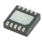
| 产品图片 |
|
| rohs | 符合RoHS无铅 / 符合限制有害物质指令(RoHS)规范要求 |
| 产品系列 | 电源管理 IC,低压差稳压器,ON Semiconductor NCV8537MN500R2G- |
| 数据手册 | |
| 产品型号 | NCV8537MN500R2G |
| 产品种类 | 低压差稳压器 |
| 供应商器件封装 | 10-DFN(3x3) |
| 其它名称 | NCV8537MN500R2GOSCT |
| 包装 | 剪切带 (CT) |
| 商标 | ON Semiconductor |
| 回动电压—最大值 | 340 mV |
| 安装类型 | 表面贴装 |
| 安装风格 | SMD/SMT |
| 封装 | Reel |
| 封装/外壳 | 10-VFDFN 裸露焊盘 |
| 封装/箱体 | DFN-10 |
| 工作温度 | -40°C ~ 125°C |
| 工厂包装数量 | 3000 |
| 最大工作温度 | + 125 C |
| 最大输入电压 | 16 V |
| 最小工作温度 | - 40 C |
| 标准包装 | 1 |
| 电压-跌落(典型值) | - |
| 电压-输入 | 5.4 V ~ 12 V |
| 电压-输出 | 5V |
| 电压调节准确度 | +/- 0.9 % |
| 电流-输出 | 500mA |
| 电流-限制(最小值) | - |
| 稳压器拓扑 | 正,固定式 |
| 稳压器数 | 1 |
| 系列 | NCV8537 |
| 负载调节 | 0.04 mV/mA |
| 输出电压 | 5 V |
| 输出电流 | 700 mA |
| 输出端数量 | 1 Output |
| 输出类型 | Fixed |


- 商务部:美国ITC正式对集成电路等产品启动337调查
- 曝三星4nm工艺存在良率问题 高通将骁龙8 Gen1或转产台积电
- 太阳诱电将投资9.5亿元在常州建新厂生产MLCC 预计2023年完工
- 英特尔发布欧洲新工厂建设计划 深化IDM 2.0 战略
- 台积电先进制程称霸业界 有大客户加持明年业绩稳了
- 达到5530亿美元!SIA预计今年全球半导体销售额将创下新高
- 英特尔拟将自动驾驶子公司Mobileye上市 估值或超500亿美元
- 三星加码芯片和SET,合并消费电子和移动部门,撤换高东真等 CEO
- 三星电子宣布重大人事变动 还合并消费电子和移动部门
- 海关总署:前11个月进口集成电路产品价值2.52万亿元 增长14.8%


PDF Datasheet 数据手册内容提取
NCV8537 Linear Regulator - High Accuracy, Low Dropout, Power Good Function 500 mA www.onsemi.com The NCV8537 is a high performance low dropout linear voltage regulator. Based on the popular NCV8535, the device retains all the best features of its predecessor which includes high accuracy, excellent stability, low noise performance and reverse bias protection but now includes a Power Good output signal to enable monitoring of DFN10 DFNW10 the supply system. The device is available with fixed or adjustable CASE 485C CASE 507AM outputs and is packaged in a 10 pin 3x3 mm DFN package. Features PIN CONFIGURATION • High Accuracy Output Over Line and Load Variances (±0.9% at 25°C) Pin 1, 2. Vout • Operating Temperature Range: −40°C to 125°C 3. Sense / ADJ 4. GND • Power Good Output to Indicate the Regulator is Within Specified 5. PWRG Limits 6. NC • 7. NR Stable Output with Low Value Capacitors of any type and with no 8. SD Minimum Load Current Requirement 9, 10. Vin • Incorporates Current Limiting and Reverse Bias Protection EP, GND • Thermal Shutdown Protection • MARKING DIAGRAM Low Dropout Voltage at Full Load (340 mV typ at V = 3.3 V) o • Low Noise (33 (cid:2)Vrms w/ 10 nF Cnr and 52 (cid:2)Vrms w/out Cnr) 1 V8537 1 L8537 • Low Shutdown Current (< 1 mA) xxx xxx • Reverse Bias Protected ALYW(cid:2) ALYW(cid:2) (cid:2) (cid:2) • 2.9 V to 12 V Supply Range • Available in 1.8 V, 2.5 V, 3.3 V, 5.0 V and Adjustable Output V8537= Specific Device Code Voltages L8537= Specific Device Code • NCV Prefix for Automotive and Other Applications Requiring xxx = ADJ, 180, 250, 330, 500 A = Assembly Location Unique Site and Control Change Requirements; AEC−Q100 L = Wafer Lot Qualified and PPAP Capable Y = Year • These are Pb−Free Devices W = Work Week (cid:2) = Pb−Free Package Applications (Note: Microdot may be in either location) • Networking Systems, DSL/Cable Modems • Audio Systems for Automotive Applications • ORDERING INFORMATION Navigation Systems See detailed ordering, marking and shipping information in the • Satellite Receivers package dimensions section on page 15 of this data sheet. © Semiconductor Components Industries, LLC, 2017 1 Publication Order Number: October, 2019 − Rev. 6 NCV8537/D
NCV8537 Cnr ON (Optional) 6 7 OFF 8 NC NR SD SENSE 3 9 IN OUT 2 10 Vin IN OUT Vout 1 + + 1.0 C(cid:2)iFn R1 PWRG EP GND 1.0C (cid:2)ouFt 100k 5 EP 4 PWRG Figure 1. Typical Fixed Version Application Schematic Cnr R2 ON (Optional) 6 7 OFF 8 NC NR 3 SD ADJ 9 2 R3 IN OUT 10 1 Vin IN OUT Vout + + Cout 1.0 C(cid:2)iFn R1010k P5WRG EPEP G4ND 1.0 (cid:2)F PWRG Figure 2. Typical Adjustable Version Application Schematic www.onsemi.com 2
NCV8537 Comp. PWRG Vin Enable Voltage SD Block Reference Current and Series Pass Thermal Error NR Protection Amplifier REelevmeresnet Bwiiaths Vout Circuit Protection NCV8537 Adjustable ADJ GND Figure 3. Block Diagram, Adjustable Output Version Comp. PWRG Vin Enable Voltage SD Block Reference Current and Series Pass NR PTrohteercmtiaoln AmErprolifrier REelevmeresnet Bwiiaths Vout Circuit Protection SENSE NCV8537 Fix GND Figure 4. Block Diagram, Fixed Output Version www.onsemi.com 3
NCV8537 PIN FUNCTION DESCRIPTION Pin No. Pin Name Description 1, 2 Vout Regulated output voltage. Bypass to ground with Cout (cid:2) 1.0 (cid:2)F 3 SENSE/ADJ For output voltage sensing, connect to Pins 1 and 2.at Fixed output Voltage version Adjustable pin at Adjustable output version 4 GND Power Supply Ground 5 PWRG Power Good 6 NC Not Connected 7 NR Noise Reduction Pin. This is an optional pin used to further reduce noise. 8 SD Shutdown pin. When not in use, this pin should be connected to the input pin. 9, 10 Vin Power Supply Input Voltage EPAD EPAD Exposed thermal pad should be connected to ground. MAXIMUM RATINGS Rating Symbol Value Unit Input Voltage Vin −0.3 to +16 V Output Voltage Vout −0.3 to Vin +0.3 or 10 V* V PWRG Pin Voltage VPWRG −0.3 to +16 V Shutdown Pin Voltage Vsh −0.3 to +16 V Junction Temperature Range TJ −40 to +150 °C Storage Temperature Range Tstg −50 to +150 °C Stresses exceeding those listed in the Maximum Ratings table may damage the device. If any of these limits are exceeded, device functionality should not be assumed, damage may occur and reliability may be affected. NOTE: This device series contains ESD protection and exceeds the following tests: Human Body Model (HBM) tested per AEC−Q100−002 (EIA/JESD22−A114) Machine Model (MM) tested per AEC−Q100−003 (EIA/JESD22−A115) Charged Device Model (CDM) tested per EIA/JESD22−C101. *Which ever is less. Reverse bias protection feature valid only if (Vout − Vin) ≤ 7 V. THERMAL CHARACTERISTICS Test Conditions (Typical Value) Characteristic Min Pad Board (Note 1) 1(cid:2) Pad Board (Note 1) Unit Junction−to−Air, (cid:3)JA 215 66 °C/W Junction−to−Pin, J−L4 58 18 °C/W 1. As mounted on a 35 x 35 x 1.5 mm FR4 Substrate, with a single layer of a specified copper area of 2 oz (0.07 mm thick) copper traces and heat spreading area. JEDEC 51 specifications for a low and high conductivity test board recommend a 2 oz copper thickness. Test conditions are under natural convection or zero air flow. www.onsemi.com 4
NCV8537 ELECTRICAL CHARACTERISTICS − 1.8 V (Vout = 1.8 V typical, Vin = 2.9 V, TA = −40°C to +125°C, unless otherwise noted, Note 2) Characteristic Symbol Min Typ Max Unit Output Voltage (Accuracy) Vout −0.9% 1.8 +0.9% V Vin = 2.9 V to 5.8 V, Iload = 0.1 mA to 500 mA, TA = 25°C 1.783 1.817 Output Voltage (Accuracy) Vout −1.4% 1.8 +1.4% V Vin = 2.9 V to 5.8 V, Iload = 0.1 mA to 500 mA, TA = 0°C to +85°C 1.774 1.826 Output Voltage (Accuracy) Vout −1.5% 1.8 +1.5% V Vin = 2.9 V to 5.8 V, Iload = 0.1 mA to 500 mA, TA = −40°C to +125°C 1.773 1.827 Minimum Input Voltage Vinmin 2.9 V Line Regulation LineReg 0.04 mV/V Vin = 2.9 V to 12 V, Iload = 0.1 mA Load Regulation LoadReg 0.04 mV/mA Vin = 2.9 V, Iload = 0.1 mA to 500 mA Dropout Voltage (See Figure 9) VDO mV Iload = 500 mA (Notes 3, 4) 620 Iload = 300 mA (Notes 3, 4) 230 Iload = 50 mA (Notes 3, 4) 95 Peak Output Current (See Figures 14 and 17) Ipk 500 700 830 mA Short Output Current (See Figure 14) Vin < 7 V, TA = 25°C Isc 900 mA Thermal Shutdown / Hysteresis TJ 160/10 °C Ground Current IGND In Regulation Iload = 500 mA (Note 3) 9.0 14 mA Iload = 300 mA (Note 3) 4.6 7.5 Iload = 50 mA 0.8 2.5 Iload = 0.1 mA − 220 (cid:2)A In Dropout Vin = 2.2 V, Iload = 0.1 mA 500 (cid:2)A In Shutdown VSD = 0 V IGNDsh 1.0 (cid:2)A Output Noise Vnoise Cnr = 0 nF, Iload = 500 mA, f = 10 Hz to 100 kHz, Cout = 10 (cid:2)F 52 (cid:2)Vrms Cnr = 10 nF, Iload = 500 mA, f = 10 Hz to 100 kHz, Cout = 10 (cid:2)F 33 (cid:2)Vrms Power Good Voltage Velft % of Low Threshold 93 95 Vout Hysteresis 2 High Threshold 97 99 Power Good Pin Voltage Saturation (Ief − 1.0 mA) Vefdo 200 mV Power Good Pin Leakage Iefleak 1.0 (cid:2)A Power Good Blanking Time (Note 7) tef 50 (cid:2)s Shutdown VSD Threshold Voltage ON 2.0 V Threshold Voltage OFF 0.4 V SD Input Current, VSD = 0 V to 0.4 V or VSD = 2.0 V to Vin ISD 0.07 1.0 (cid:2)A Output Current In Shutdown Mode, Vout = 0 V IOSD 0.07 1.0 (cid:2)A Reverse Bias Protection, Current Flowing from the Output Pin to GND IOUTR 10 (cid:2)A (Vin = 0 V, Vout_forced = 1.8 V) 2. Performance guaranteed over the operating temperature range by design and/or characterization, production tested at TJ = TA = 25°C. Low duty cycle pulse techniques are used during testing to maintain the junction temperature as close to ambient as possible. 3. TA must be greater than 0°C. 4. Maximum dropout voltage is limited by minimum input voltage Vin = 2.9 V recommended for guaranteed operation. www.onsemi.com 5
NCV8537 ELECTRICAL CHARACTERISTICS − 2.5 V (Vout = 2.5 V typical, Vin = 2.9 V, TA = −40°C to +125°C, unless otherwise noted, Note 5) Characteristic Symbol Min Typ Max Unit Output Voltage (Accuracy) Vout −0.9% 2.5 +0.9% V Vin = 2.9 V to 6.5 V, Iload = 0.1 mA to 500 mA, TA = 25°C 2.477 2.523 Output Voltage (Accuracy) Vout −1.4% 2.5 +1.4% V Vin = 2.9 V to 6.5 V, Iload = 0.1 mA to 500 mA, TA = 0°C to +85°C 2.465 2.535 Output Voltage (Accuracy) Vout −1.5% 2.5 +1.5% V Vin = 2.9 V to 6.5 V, Iload = 0.1 mA to 500 mA, TA = −40°C to +125°C 2.462 2.538 Minimum Input Voltage Vinmin 2.9 V Line Regulation LineReg 0.04 mV/V Vin = 2.9 V to 12 V, Iload = 0.1 mA Load Regulation LoadReg 0.04 mV/mA Vin = 2.9 V, Iload = 0.1 mA to 500 mA Dropout Voltage (See Figure 10) VDO mV Iload = 500 mA (Note 6) 340 Iload = 300 mA (Note 6) 230 Iload = 50 mA 110 Iload = 0.1mA 10 Peak Output Current (See Figures 14 and 18) Ipk 500 700 800 mA Short Output Current (See Figure 14) Vin < 7 V, TA = 25°C Isc 900 mA Thermal Shutdown / Hysteresis TJ 160/10 °C Ground Current IGND In Regulation Iload = 500 mA (Note 6) 9.0 14 mA Iload = 300 mA (Note 6) 4.6 7.5 Iload = 50 mA 0.8 2.5 Iload = 0.1 mA − 220 (cid:2)A In Dropout Vin = 2.4 V, Iload = 0.1 mA 500 (cid:2)A In Shutdown VSD = 0 V IGNDsh 1.0 (cid:2)A Output Noise Vnoise Cnr = 0 nF, Iload = 500 mA, f = 10 Hz to 100 kHz, Cout = 10 (cid:2)F 56 (cid:2)Vrms Cnr = 10 nF, Iload = 500 mA, f = 10 Hz to 100 kHz, Cout = 10 (cid:2)F 35 (cid:2)Vrms Power Good Voltage Velft % of Low Threshold 93 95 Vout Hysteresis 2 High Threshold 97 99 Power Good Pin Voltage Saturation (Ief − 1.0 mA) Vefdo 200 mV Power Good Pin Leakage Iefleak 1.0 (cid:2)A Power Good Blanking Time (Note 7) tef 50 (cid:2)s Shutdown VSD Threshold Voltage ON 2.0 V Threshold Voltage OFF 0.4 V SD Input Current, VSD = 0 V to 0.4 V or VSD = 2.0 V to Vin ISD 0.07 1.0 (cid:2)A Output Current In Shutdown Mode, Vout = 0 V IOSD 0.07 1.0 (cid:2)A Reverse Bias Protection, Current Flowing from the Output Pin to GND IOUTR 10 (cid:2)A (Vin = 0 V, Vout_forced = 2.5 V) 5. Performance guaranteed over the operating temperature range by design and/or characterization, production tested at TJ = TA = 25°C. Low duty cycle pulse techniques are used during testing to maintain the junction temperature as close to ambient as possible. 6. TA must be greater than 0°C. 7. Can be disabled per customer request. www.onsemi.com 6
NCV8537 ELECTRICAL CHARACTERISTICS − 3.3 V (Vout = 3.3 V typical, Vin = 3.7 V, TA = −40°C to +125°C, unless otherwise noted, Note 8) Characteristic Symbol Min Typ Max Unit Output Voltage (Accuracy) Vin Vout −0.90% 3.3 0.90% V Vin = 3.7 V to 7.3 V, Iload = 0.1 mA to 500 mA, TA = 25°C 3.27 3.33 Output Voltage (Accuracy) Vout −1.40% 3.3 1.40% V Vin = 3.7 V to 7.3 V, Iload = 0.1 mA to 500 mA, TA = 0°C to +85°C 3.254 3.346 Output Voltage (Accuracy) Vout −1.50% 3.3 1.50% V Vin = 3.7 V to 7.3 V, Iload = 0.1 mA to 500 mA, TA = −40°C to +125°C 3.25 3.35 Line Regulation LineReg 0.04 mV/V Vin = 3.7 V to 12 V, Iload = 0.1 mA Load Regulation LoadReg 0.04 mV/mA Vin = 3.7 V, Iload = 0.1 mA to 500 mA Dropout Voltage VDO mV Iload = 500 mA 340 Iload = 300 mA 230 Iload = 50 mA 110 Iload = 0.1 mA 10 Peak Output Current (See Figure 14) Ipk 500 700 800 mA Short Output Current (See Figure 14) Vin < 7 V, TA = 25°C Isc 900 mA Thermal Shutdown / Hysteresis TJ 160/10 °C Ground Current IGND In Regulation Iload = 500 mA (Note 8) 9 14 mA Iload = 300 mA 4.6 7.5 Iload = 50 mA 0.8 2.5 Iload = 0.1 mA − 220 (cid:2)A In Dropout Vin = 3.7 V, Iload = 0.1 mA 500 (cid:2)A In Shutdown VSD = 0 V IGNDsh 1 (cid:2)A Output Noise Vnoise (cid:2)Vrms Cnr = 0 nF, Iload = 500 mA, f = 10 Hz to 100 kHz, Cout = 10 (cid:2)F 69 Cnr = 10 nF, Iload = 500 mA, f = 10 Hz to 100 kHz, Cout = 10 (cid:2)F 46 Power Good Voltage Velft % of Low Threshold 93 95 Vout Hysteresis 2 High Threshold 97 99 Power Good Pin Voltage Saturation (Ief = 1.0 mA) Vefdo 200 mV Power Good Pin Leakage Iefleak 1 (cid:2)A Power Good Blanking Time (Note 9) tef 50 (cid:2)s Shutdown VSD V Threshold Voltage ON 2 Threshold Voltage OFF 0.4 SD Input Current, VSD = 0 V to 0.4 V or VSD = 2.0 V to Vin ISD 0.07 1 (cid:2)A Output Current In Shutdown Mode, Vout = 0 V IOSD 0.07 1 (cid:2)A Reverse Bias Protection, Current Flowing from the Output Pin to GND IOUTR 10 (cid:2)A (Vin = 0 V, Vout_forced = 3.3 V) 8. Performance guaranteed over the operating temperature range by design and/or characterization, production tested at TJ = TA = 25°C. Low duty cycle pulse techniques are used during testing to maintain the junction temperature as close to ambient as possible. 9. Can be disabled per customer request. www.onsemi.com 7
NCV8537 ELECTRICAL CHARACTERISTICS − 5 V (Vout = 5.0 V typical, Vin = 5.4 V, TA = −40°C to +125°C, unless otherwise noted, Note 10) Characteristic Symbol Min Typ Max Unit Output Voltage (Accuracy) Vin Vout −0.90% 5 0.90% V Vin = 5.4 V to 7.3 V, Iload = 0.1 mA to 500 mA, TA = 25°C 4.955 5.045 Output Voltage (Accuracy) Vout −1.40% 5 1.40% V Vin = 5.4 V to 7.3 V, Iload = 0.1 mA to 500 mA, TA = 0°C to +85°C 4.93 5.07 Output Voltage (Accuracy) Vout −1.50% 5 1.50% V Vin = 5.4 V to 7.3 V, Iload = 0.1 mA to 500 mA, TA = −40°C to +125°C 4.925 5.075 Line Regulation LineReg 0.04 mV/V Vin = 5.4 V to 12 V, Iload = 0.1 mA Load Regulation LoadReg 0.04 mV/mA Vin = 5.4 V, Iload = 0.1 mA to 500 mA Dropout Voltage VDO mV Iload = 500 mA 340 Iload = 300 mA 230 Iload = 50 mA 110 Iload = 0.1 mA 10 Peak Output Current (See Figure 14) Ipk 500 700 830 mA Short Output Current (See Figure 14) Vin < 7 V, TA = 25°C Isc 930 mA Thermal Shutdown / Hysteresis TJ 160/10 °C Ground Current IGND In Regulation Iload = 500 mA (Note 10) 9 14 mA Iload = 300 mA 4.6 7.5 Iload = 50 mA 0.8 2.5 Iload = 0.1 mA − 220 (cid:2)A In Dropout Vin = 3.2 V, Iload = 0.1 mA 500 (cid:2)A In Shutdown VSD = 0 V IGNDsh 1 (cid:2)A Output Noise Vnoise (cid:2)Vrms Cnr = 0 nF, Iload = 500 mA, f = 10 Hz to 100 kHz, Cout = 10 (cid:2)F 93 Cnr = 10 nF, Iload = 500 mA, f = 10 Hz to 100 kHz, Cout = 10 (cid:2)F 58 Power Good Voltage Velft % of Low Threshold 93 95 Vout Hysteresis 2 High Threshold 97 99 Power Good Pin Voltage Saturation (Ief = 1.0 mA) Vefdo 200 mV Power Good Pin Leakage Iefleak 1 (cid:2)A Power Good Blanking Time (Note 11) tef 50 (cid:2)s Shutdown VSD V Threshold Voltage ON 2 Threshold Voltage OFF 0.4 SD Input Current, VSD = 0 V to 0.4 V or VSD = 2.0 V to Vin ISD 0.07 1 (cid:2)A Output Current In Shutdown Mode, Vout = 0 V IOSD 0.07 1 (cid:2)A Reverse Bias Protection, Current Flowing from the Output Pin to GND IOUTR 10 (cid:2)A (Vin = 0 V, Vout_forced = 5 V) 10.Performance guaranteed over the operating temperature range by design and/or characterization, production tested at TJ = TA = 25°C. Low duty cycle pulse techniques are used during testing to maintain the junction temperature as close to ambient as possible. 11.Can be disabled per customer request. www.onsemi.com 8
NCV8537 ELECTRICAL CHARACTERISTICS − ADJUSTABLE (Vout = 1.25 V typical, Vin = 2.9 V, TA = −40°C to +125°C, unless otherwise noted, Note 12) Characteristic Symbol Min Typ Max Unit Reference Voltage (Accuracy) Vref −0.90% 1.25 0.90% V Vin = 2.9 V to Vout +4.0 V, Iload = 0.1 mA to 500 mA, TA = 25°C 1.239 1.261 Reference Voltage (Accuracy) Vref −1.40% 1.25 1.40% V Vin = 2.9 V to Vout + 4.0 V, Iload = 0.1 mA to 500 mA, TA = 0°C to +85°C 1.233 1.268 Reference Voltage (Accuracy) Vref −1.50% 1.25 1.50% V Vin = 2.9 V to Vout + 4.0 V, Iload = 0.1 mA to 500 mA, TA = −40°C to 1.231 1.269 +125°C Line Regulation LineReg 0.04 mV/V Vin = 2.9 V to 12 V, Iload = 0.1 mA Load Regulation LoadReg 0.04 mV/mA Vin = 2.9 V to 12 V, Iload = 0.1 mA to 500 mA Dropout Voltage (Vout = 2.5 V − 10 V) VDO mV Iload = 500 mA 340 Iload = 300 mA 230 Iload = 50 mA 110 Iload = 0.1 mA 10 Peak Output Current (See Figure 14) Ipk 500 700 830 mA Short Output Current (See Figure 14) Vin < 7 V, TA = 25°C Isc mA Vout (cid:3) 3.3 V 900 Vout > 3.3 V 930 Thermal Shutdown / Hysteresis TJ 160/ °C 10 Ground Current IGND In Regulation Iload = 500 mA (Note 12) 9 14 mA Iload = 300 mA 4.6 7.5 Iload = 50 mA 0.8 2.5 Iload = 0.1 mA 220 (cid:2)A In Dropout Vin = Vout + 0.1 V or 2.9 V (whichever is higher), Iload = 0.1 mA 500 (cid:2)A In Shutdown VSD = 0 V IGNDsh 1 (cid:2)A Output Noise Vnoise (cid:2)Vrms Cnr = 0 nF, Iload = 500 mA, f = 10 Hz to 100 kHz, Cout = 10 (cid:2)F 69 Cnr = 10 nF, Iload = 500 mA, f = 10 Hz to 100 kHz, Cout = 10 (cid:2)F 46 Power Good Voltage Velft % of Low Threshold 93 95 Vout Hysteresis 2 High Threshold 97 99 Power Good Pin Voltage Saturation (Ief = 1.0 mA) Vefdo 200 mV Power Good Pin Leakage Iefleak 1 (cid:2)A Power Good Pin Blanking Time (Note 13) tef 50 (cid:2)s Shutdown VSD V Threshold Voltage ON 2 Threshold Voltage OFF 0.4 SD Input Current, VSD = 0 V to 0.4 V or VSD = 2.0 V to Vin ISD (cid:2)A Vin (cid:3) 5.4 V 0.07 1 Vin > 5.4 V 5 Output Current In Shutdown Mode, Vout = 0 V IOSD 0.07 1 (cid:2)A Reverse Bias Protection, Current Flowing from the Output Pin to GND IOUTR 1 (cid:2)A (Vin = 0 V, Vout_forced = Vout (nom) (cid:3) 7 V) 12.Performance guaranteed over the operating temperature range by design and/or characterization, production tested at TJ = TA = 25°C. Low duty cycle pulse techniques are used during testing to maintain the junction temperature as close to ambient as possible. 13.Can be disabled per customer request. www.onsemi.com 9
NCV8537 1.85 2.52 1.84 VIN = 2.9 V 2.515 VIN = 2.9 V V) IOUT = 0 V) IOUT = 0 E ( 1.83 E ( 2.51 G G A 1.82 A 2.505 T T L L O 1.81 O 2.5 T V 1.8 T V 2.495 VOUT = 2.5 V U U TP 1.79 VOUT = 1.8 V TP 2.49 U U O 1.78 O 2.485 , T , T U U O 1.77 O 2.48 V V 1.76 2.475 1.75 2.47 −40 −20 0 20 40 60 80 100 120 140 −40 −20 0 20 40 60 80 100 120 140 TA, TEMPERATURE (°C) TA, TEMPERATURE (°C) Figure 5. Output Voltage vs. Temperature Figure 6. Output Voltage vs. Temperature 1.8 V Version 2.5 V Version 3.320 5.1 3.315 VIN = 3.7 V VIN = 5.4 V E (V) 3.310 IOUT = 0 E (V) 5.05 IOUT = 0 G 3.305 G A A T T L 3.300 L 5 O O T V 3.295 VOUT = 3.3 V T V VOUT = 5.0 V U U P 3.290 P 4.95 T T U U O 3.285 O , UT3.280 , UT 4.9 O O V V 3.275 3.270 4.85 −40 −20 0 20 40 60 80 100 120 140 −40 −20 0 20 40 60 80 100 120 140 TA, TEMPERATURE (°C) TA, TEMPERATURE (°C) Figure 7. Output Voltage vs. Temperature 3.3 V Figure 8. Output Voltage vs. Temperature 5.0 V Version Version 900 400 V) 800 V) 350 m m E ( 700 E ( 300 G G 500 mA TA 600 TA L L 250 O O V 500 500 mA V 300 mA T T 200 U 400 U O O P P 150 O 300 300 mA O R R 50 mA D D 100 , O 200 50 mA , O D D V 100 V 50 0 0 0 20 40 60 80 100 120 140 0 20 40 60 80 100 120 140 TA, TEMPERATURE (°C) TA, TEMPERATURE (°C) Figure 9. Dropout Voltage vs. Temperature Figure 10. Dropout Voltage vs. Temperature 1.8 V Version 2.5 V Version www.onsemi.com 10
NCV8537 400 350 mV) 350 mV) 300 500 mA E ( 300 500 mA E ( G G 250 A A T T L 250 L 300 mA O 300 mA O 200 V V T 200 T U U O O 150 P 150 P O 50 mA O 50 mA R R 100 D 100 D , O , O VD 50 VD 50 0 0 0 20 40 60 80 100 120 140 0 20 40 60 80 100 120 140 TA, TEMPERATURE (°C) TA, TEMPERATURE (°C) Figure 11. Dropout Voltage vs. Temperature Figure 12. Dropout Voltage vs. Temperature 3.3 V Version 5.0 V Version 1000 900 0.97 Vout 800 Isc A) 700 A), I (msc 560000 Ipk (V)out m 400 V (pk 300 I 200 VIN = 2.9 V 100 VOUT = 1.8 V 0 0 20 40 60 80 100 120 140 Iout (mA) Ipk Isc TA, TEMPERATURE (°C) (For specific values of Ipk and Isc, please refer to Figure 13) Figure 13. Peak and Short Current Figure 14. Output Voltage vs. Output Current vs. Temperature 12 12 mA) 10 VVOIUNT = = 2 1.9.8 V V mA) 10 VVOIUNT = = 2 1.9.8 V V T ( T ( TA = 25°C N 500 mA N E 8 E 8 R R R R U U C 6 C 6 D 300 mA D N N U U O 4 O 4 R R G G , ND 2 , ND 2 G 50 mA G I I 0 0 0 20 40 60 80 100 120 140 0 0.1 0.2 0.3 0.4 0.5 TA, TEMPERATURE (°C) IOUT, OUTPUT CURRENT (A) Figure 15. Ground Current vs. Temperature Figure 16. Ground Current vs. Output Current www.onsemi.com 11
NCV8537 0.8 0.8 0.7 25°C 0°C 0.7 25°C 0°C A) A) T ( 0.6 T ( 0.6 N N E E RR 0.5 −20°C RR 0.5 −20°C −40°C U U T C 0.4 −40°C T C 0.4 U U TP 0.3 TP 0.3 U U O O , T 0.2 , T 0.2 IOU 0.1 VVOIUNT = = 2 1.9.8 V V IOU 0.1 VVOIUNT = = 2 2.9.5 V V 0.0 0.0 3.6 3.4 3.2 3 2.8 2.6 2.4 2.2 3.5 3.4 3.3 3.2 3.1 3 2.9 2.8 2.7 VIN, INPUT VOLTAGE (V) VIN, INPUT VOLTAGE (V) Figure 17. Output Current Capability for the Figure 18. Output Current Capability for the 1.8 V Version 2.5 V Version 100 90 dB) 90 dB) 80 VIN = 3.4 VVO +U0T.5 = V 2P.5P VModulation N ( 80 N ( 70 TA = 25°C CTIO 70 Iout = 50 mA CTIO 60 Iout = 50 mA E 60 E REJ 50 Iout = 0.5 A REJ 50 E E 40 PL 40 PL RIP 30 Iout = 0.25 A RIP 30 Iout = 0.5 A RR, 20 VIN = 2.9 V +0.5 VPP Modulation RR, 20 Iout = 0.25 A PS 10 VOTUAT = = 2 15.°2C5 V PS 10 0 0 100 1k 10k 100k 1M 100 1k 10k 100k 1M F, FREQUENCY (Hz) F, FREQUENCY (Hz) Figure 20. PSRR vs. Frequency Adjustable Figure 21. PSRR vs. Frequency 2.5 V Version Version 600 600 500 500 Z) Z) H H √ √ V/ 400 V/ 400 n n Y ( Cnr = 0 nF Y ( Cnr = 0 nF T T SI 300 SI 300 N N E E D D E 200 Cnr = 10 nF E 200 Cnr = 10 nF S S NOI 100 VIN = 2.9 V NOI 100 VIN = 2.9 V VOUT = 1.25 V VOUT = 2.5 V TA = 25°C TA = 25°C 0 0 10 100 1k 10k 100k 1M 10 100 1k 10k 100k 1M F, FREQUENCY (Hz) F, FREQUENCY (Hz) Figure 22. Output Noise Density Adjustable Figure 23. Output Noise Density 2.5 V Version Version www.onsemi.com 12
NCV8537 Figure 24. Power Good Activation Figure 25. Power Good Inactivation 15 300 Vin at2 D5°aCta, 1S h(cid:2)eFe Ct Taepsatc Citaonncdeitions, 250 (cid:4)) SR ( 10 W) 200 M E °C/ 150 MU Unstable Area JA ( 1 oz CF AXI 5.0 (cid:3) 100 M 2 oz CF 50 Stable Area 0 0 0 100 200 300 400 500 0 100 200 300 400 500 600 700 OUTPUT CURRENT (mA) COPPER HEAT SPREADING AREA (mm2) Figure 26. Stability with ESR vs. Output Figure 27. DFN10 Self−Heating Thermal Current Characterstics as a Function of Copper Area on the PCB NOTE: Typical characteristics were measured with the same conditions as electrical characteristics. www.onsemi.com 13
NCV8537 APPLICATIONS INFORMATION Reverse Bias Protection temperature is exceeded. This feature provides protection Reverse bias is a condition caused when the input voltage from a catastrophic device failure due to accidental goes to zero, but the output voltage is kept high either by a overheating. This protection feature is not intended to be used large output capacitor or another source in the application as a substitute to heat sinking. The maximum power that can which feeds the output pin. be dissipated, can be calculated with the equation below: Normally in a bipolar LDO all the current will flow from TJ(max)(cid:5)TA the output pin to input pin through the PN junction with PD(cid:4) (eq. 1) R(cid:3)JA limited current capability and with the potential to destroy For improved thermal performance, contact the factory the IC. for the DFN package option. The DFN package includes an Due to an improved architecture, the NCV8537 can exposed metal pad that is specifically designed to reduce the withstand up to 7.0 V on the output pin with virtually no current flowing from output pin to input pin, and only junction to air thermal resistance, R(cid:3)JA. negligible amount of current (tens of (cid:2)A) flowing from the Adjustable Operation output pin to ground for infinite duration. The output voltage can be set by using a resistor divider as shown in Figure 2 with a range of 1.25 to 10 V. The Input Capacitor An input capacitor of at least 1.0 (cid:2)F, any type, is appropriate resistor divider can be found by solving the equation below. The recommended current through the recommended to improve the transient response of the resistor divider is from 10 (cid:2)A to 100 (cid:2)A. This can be regulator and/or if the regulator is located more than a few accomplished by selecting resistors in the k(cid:4) range. As inches from the power source. It will also reduce the circuit’s result, the I * R2 becomes negligible in the equation and sensitivity to the input line impedance at high frequencies. adj can be ignored. The capacitor should be mounted with the shortest possible track length directly across the regular’s input terminals. Vout(cid:4)1.25*(1(cid:6)R3(cid:7)R2)(cid:6)Iadj*R2 (eq. 2) Output Capacitor Power Good Operation The NCV8537 remains stable with any type of capacitor The Power Good pin on the NCV8537 will produce a as long as it fulfills its 1.0 (cid:2)F requirement. There are no logic Low when it drops below the nominal output voltage. constraints on the minimum ESR and it will remain stable up Refer to the electrical characteristics for the threshold values to an ESR of 5.0 (cid:4). Larger capacitor values will improve the at which point the Power Good goes Low. When the noise rejection and load transient response. NCV8537 is above the nominal output voltage, the Power Good will remain at logic High. Noise Reduction Pin The external pullup resistor needs to be connected Output noise can be greatly reduced by connecting a 10 nF between V and the Power Good pin. A resistor of capacitor (C ) between the noise reduction pin and ground in nr approximately 100 k(cid:4) is recommended to minimize the (see Figure 1). In applications where very low noise is not current consumption. No pullup resistor is required if the required, the noise reduction pin can be left unconnected. Power Good output is not being used. The Power Good does Dropout Voltage not function during thermal shutdown and when the part is The voltage dropout is measured at 97% of the nominal disabled. output voltage. Thermal Considerations Internal thermal limiting circuitry is provided to protect the integrated circuit in the event that the maximum junction www.onsemi.com 14
NCV8537 ORDERING INFORMATION Device* Voltage Option Marking Package Package Shipping† NCV8537MN180R2G 1.8 V V8537 180 NCV8537MN250R2G 2.5 V V8537 250 DFN10 Non−Wettable NCV8537MN330R2G 3.3 V V8537 330 3000 / Tape & Reel (Pb−Free) Flank NCV8537MN500R2G 5.0 V V8537 500 NCV8537MNADJR2G Adj V8537 ADJ NCV8537ML180R2G 1.8 V L8537 180 NCV8537ML250R2G 2.5 V L8537 250 DFN10 Wettable Flank NCV8537ML330R2G 3.3 V L8537 330 3000 / Tape & Reel (Pb−Free) SLP Process NCV8537ML500R2G 5.0 V L8537 500 NCV8537MLADJR2G Adj L8537 ADJ †For information on tape and reel specifications, including part orientation and tape sizes, please refer to our Tape and Reel Packaging Specifications Brochure, BRD8011/D. *NCV Prefix for Automotive and Other Applications Requiring Unique Site and Control Change Requirements; AEC−Q100 Qualified and PPAP Capable. www.onsemi.com 15
NCV8537 PACKAGE DIMENSIONS DFN10, 3x3, 0.5P CASE 485C ISSUE E D A NOTES: L L 1. DIMENSIONING AND TOLERANCING PER ASME Y14.5M, 1994. B 2. CONTROLLING DIMENSION: MILLIMETERS. 3. DIMENSION b APPLIES TO PLATED TERMINAL AND IS L1 MEASURED BETWEEN 0.25 AND 0.30 MM FROM TERMINAL. 4. COPLANARITY APPLIES TO THE EXPOSED PAD AS WELL AS ALTERNATE A−1 ALTERNATE A−2 THE TERMINALS. 5. TERMINAL b MAY HAVE MOLD COMPOUND MATERIAL ALONG PIN ONE ÇÇÇ E ALTERDNEATTAE ITLE RAMINAL SOINDTEO E BDOGTET. OMMO LSDU RFLFAASCHEI NOGF TMEARYM NINOATL E bX.CEED 30 MICRONS REFERENCE CONSTRUCTIONS 6. FOR DEVICE OPN CONTAINING W OPTION, DETAIL A AND B ÇÇÇ ALTERNATE CONSTRUCTION ARE NOT APPLICABLE. WET- TABLE FLANK CONSTRUCTION IS DETAIL B AS SHOWN ON 2X 0.15 C ÇÇÇ SIDE VIEW OF PACKAGE. A3 EXPOSED Cu MOLD CMPD MILLIMETERS 2X 0.15 C ÉÇÉÇ ÉÉ DIM MIN MAX TOP VIEW A 0.80 1.00 ÇÇ ÇÇ A1 0.00 0.05 A1 A3 0.20 REF DETAIL B (A3) ALTERNATE B−1 ALTERNATE B−2 b 0.18 0.30 0.10 C D 3.00 BSC DETAIL B D2 2.40 2.60 A ALTERNATE E 3.00 BSC CONSTRUCTIONS E2 1.70 1.90 10X 0.08 C e 0.50 BSC SIDE VIEW A1 C SPELAATNIENG A3 K 0.19 TYP L 0.35 0.45 L1 0.00 0.03 DETAIL A D2 10XL A1 1 5 DETAIL B SOLDERING FOOTPRINT* WETTABLE FLANK OPTION CONSTRUCTION 2.64 10X 0.55 PACKAGE E2 OUTLINE K 10 6 1.90 3.30 10Xb e 0.10 C A B BOTTOM VIEW 0.05 C NOTE 3 10X 0.30 0.50 PITCH DIMENSIONS: MILLIMETERS *For additional information on our Pb−Free strategy and soldering details, please download the ON Semiconductor Soldering and Mounting Techniques Reference Manual, SOLDERRM/D. www.onsemi.com 16
NCV8537 PACKAGE DIMENSIONS DFNW10 3x3, 0.5P CASE 507AM ISSUE A ON Semiconductor and are trademarks of Semiconductor Components Industries, LLC dba ON Semiconductor or its subsidiaries in the United States and/or other countries. ON Semiconductor owns the rights to a number of patents, trademarks, copyrights, trade secrets, and other intellectual property. A listing of ON Semiconductor’s product/patent coverage may be accessed at www.onsemi.com/site/pdf/Patent−Marking.pdf. ON Semiconductor reserves the right to make changes without further notice to any products herein. ON Semiconductor makes no warranty, representation or guarantee regarding the suitability of its products for any particular purpose, nor does ON Semiconductor assume any liability arising out of the application or use of any product or circuit, and specifically disclaims any and all liability, including without limitation special, consequential or incidental damages. Buyer is responsible for its products and applications using ON Semiconductor products, including compliance with all laws, regulations and safety requirements or standards, regardless of any support or applications information provided by ON Semiconductor. “Typical” parameters which may be provided in ON Semiconductor data sheets and/or specifications can and do vary in different applications and actual performance may vary over time. All operating parameters, including “Typicals” must be validated for each customer application by customer’s technical experts. ON Semiconductor does not convey any license under its patent rights nor the rights of others. ON Semiconductor products are not designed, intended, or authorized for use as a critical component in life support systems or any FDA Class 3 medical devices or medical devices with a same or similar classification in a foreign jurisdiction or any devices intended for implantation in the human body. Should Buyer purchase or use ON Semiconductor products for any such unintended or unauthorized application, Buyer shall indemnify and hold ON Semiconductor and its officers, employees, subsidiaries, affiliates, and distributors harmless against all claims, costs, damages, and expenses, and reasonable attorney fees arising out of, directly or indirectly, any claim of personal injury or death associated with such unintended or unauthorized use, even if such claim alleges that ON Semiconductor was negligent regarding the design or manufacture of the part. ON Semiconductor is an Equal Opportunity/Affirmative Action Employer. This literature is subject to all applicable copyright laws and is not for resale in any manner. PUBLICATION ORDERING INFORMATION LITERATURE FULFILLMENT: N. American Technical Support: 800−282−9855 Toll Free ON Semiconductor Website: www.onsemi.com Literature Distribution Center for ON Semiconductor USA/Canada 19521 E. 32nd Pkwy, Aurora, Colorado 80011 USA Europe, Middle East and Africa Technical Support: Order Literature: http://www.onsemi.com/orderlit Phone: 303−675−2175 or 800−344−3860 Toll Free USA/Canada Phone: 421 33 790 2910 Fax: 303−675−2176 or 800−344−3867 Toll Free USA/Canada For additional information, please contact your local Email: orderlit@onsemi.com Sales Representative ◊ www.onsemi.com NCV8537/D 17