ICGOO在线商城 > 集成电路(IC) > PMIC - 稳压器 - 线性 > RT9053AGB

 Datasheet下载
- 型号: RT9053AGB
- 制造商: RICHTEK
- 库位|库存: xxxx|xxxx
- 要求:
| 数量阶梯 | 香港交货 | 国内含税 |
| +xxxx | $xxxx | ¥xxxx |
查看当月历史价格
查看今年历史价格
RT9053AGB产品简介:
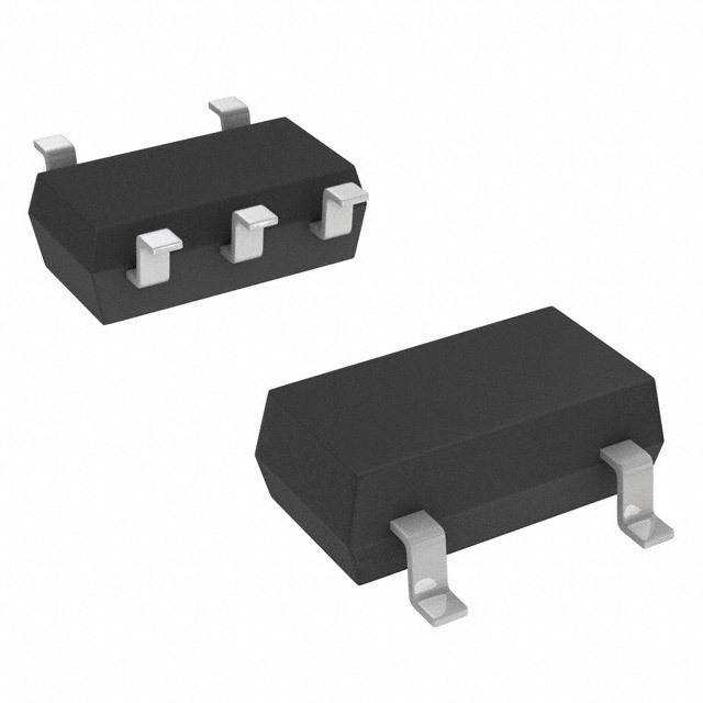
ICGOO电子元器件商城为您提供RT9053AGB由RICHTEK设计生产,在icgoo商城现货销售,并且可以通过原厂、代理商等渠道进行代购。 RT9053AGB价格参考。RICHTEKRT9053AGB封装/规格:PMIC - 稳压器 - 线性, Linear Voltage Regulator IC Positive Adjustable 1 Output Adj to 0.8V 400mA SOT-23-5。您可以下载RT9053AGB参考资料、Datasheet数据手册功能说明书,资料中有RT9053AGB 详细功能的应用电路图电压和使用方法及教程。
RT9053AGB 是由 Richtek USA Inc.(立锜科技)生产的一款线性稳压器(LDO),属于电源管理集成电路(PMIC)的一部分。该器件主要用于将较高的输入电压稳定地转换为较低的输出电压,具有低噪声、高电源抑制比(PSRR)和快速瞬态响应等特性。

 应用场景包括:

1. 便携式电子设备:如智能手机、平板电脑、电子书阅读器等,适用于需要高效能与低功耗的电池供电系统。
2. 无线通信模块:用于Wi-Fi、蓝牙、Zigbee等无线芯片组的电源管理,提供稳定的低噪声电源以提升信号质量。
3. 传感器供电:适用于高精度模拟传感器或射频传感器的供电,因其低输出噪声可提高测量精度。
4. 音频设备:如耳机放大器、麦克风偏置电源等对噪声敏感的电路中,确保音质清晰。
5. 工业控制系统:在PLC、工业仪表等设备中作为关键电源调节器件,提供可靠稳定的电压。
6. 汽车电子系统:用于车载信息娱乐系统、摄像头模块或其他对电源稳定性要求高的场合。

该器件采用小型封装(如DFN-8),适合空间受限的设计,同时具备过热保护与过流保护功能,提升了系统可靠性。
| 参数 | 数值 |
| 产品目录 | 集成电路 (IC) |
| 描述 | IC REG LDO ADJ 0.4A SOT23-5 |
| 产品分类 | |
| 品牌 | Richtek USA Inc |
| 数据手册 | http://www.richtek.com/download_ds.jsp?s=735 |
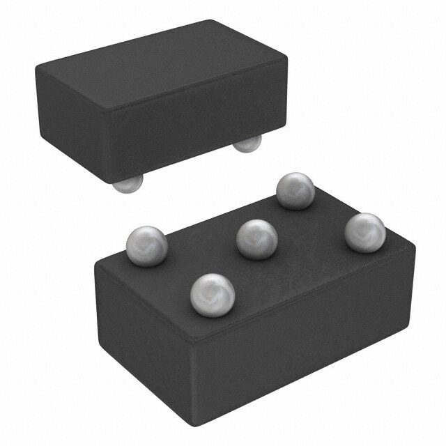
| 产品图片 |
|
| 产品型号 | RT9053AGB |
| rohs | 无铅 / 符合限制有害物质指令(RoHS)规范要求 |
| RoHS指令信息 | http://www.richtek.com/download.jsp?t=UyUyRmFzc2V0cyUyRjIwMDklMkYwNiUyRjE3JTJGcGFnZTY1MTYwenRpeGIucGRmJTNEJTNEJTNE%0AR0w5NTI1LUMtLVBiLWZyZWUrUHJvZHVjdCsrR3JlZW4rUHJvZHVjdCtTdGF0ZW1lbnQrMDkwNjE2%0AQw%3D%3D |
| 产品系列 | - |
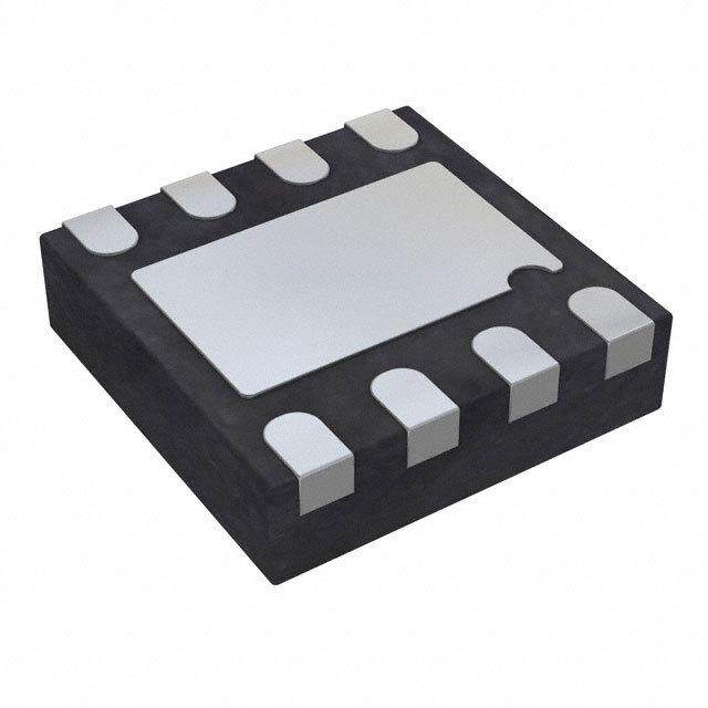
| 供应商器件封装 | SOT-23-5 |
| 其它名称 | 1028-1180-6 |
| 包装 | Digi-Reel® |
| 安装类型 | 表面贴装 |
| 封装/外壳 | SC-74A,SOT-753 |
| 工作温度 | -40°C ~ 85°C |
| 标准包装 | 1 |
| 电压-跌落(典型值) | 0.23V @ 400mA |
| 电压-输入 | 2.2 V ~ 5.5 V |
| 电压-输出 | 可调至 0.8V |
| 电流-输出 | 400mA |
| 电流-限制(最小值) | 400mA |
| 稳压器拓扑 | 正,可调式 |
| 稳压器数 | 1 |


PDF Datasheet 数据手册内容提取
® RT9053A Low Dropout, 400mA Adjustable Linear Regulator General Description Features The RT9053A is a high performance, 400mA LDO regulator Adjustable Output Voltage Down to 0.8V and ultra low dropout. The quiescent current is as low as Wide Operating Voltage Ranges : 2.2V to 5.5V 42μA, further prolonging the battery life. The RT9053A also Low Dropout : 230mV at 400mA works with low ESR ceramic capacitors, reducing the Ultra Fast Response in Line/Load Transient amount of board space necessary for power applications, Current Limiting Protection critical in handheld wireless devices. Thermal Shutdown Protection Output Only 1μμμμμF Capacitor Required for Stability The RT9053A consumes typically 0.7μA in shutdown RoHS Compliant and Halogen Free mode. The other features include low dropout voltage, high output accuracy, and current limiting protection. The Applications RT9053A is available in SOT-23-5 and WDFN-6L 2x2 Mega Sim Card packages. CDMA/GSM Cellular Handsets Portable Information Appliances Ordering Information Laptop, Palmtops, Notebook Computers RT9053A Hand-Held Instruments Package Type B : SOT-23-5 Mini PCI& PCI-Express Cards QW : WDFN- 6L 2x2 (W-Type) PCMCIA & New Cards Lead Plating System G : Green (Halogen Free and Pb Free) Pin Configurations Z : ECO (Ecological Element with Halogen Free and Pb free) (TOP VIEW) (for WDFN-6L 2x2 Only) VOUT FB Note : 5 4 EN 1 6 FB Richtek roducts are : D GND 2 N 5 NC RoHS compliant and compatible with the current require- 2 3 G VIN 3 7 4 VOUT ments of IPC/JEDEC J-STD-020. VIN GND EN Suitable for use in SnPb or Pb-free soldering processes. SOT-23-5 WDFN-6L 2x2 Marking Information RT9053AGB RT9053AGQW 3Q= : Product Code JH : Product Code 3Q=DNN DNN : Date Code JHW W : Date Code RT9053AZQW J_H : Product Code J_HW W : Date Code Copyright © 2014 Richtek Technology Corporation. All rights reserved. is a registered trademark of Richtek Technology Corporation. DS9053A-03 September 2014 www.richtek.com 1
RT9053A Typical Application Circuit RT9053A VIN CIN VIN VOUT COUT VOUT 1µF 1µF R1 Chip Enable EN FB GND R2 Functional Pin Description Pin No. Pin Name Pin Function SOT-23-5 WDFN-6L 2x2 1 3 VIN Supply Input. 2, 7 Ground. The exposed pad must be soldered to a large PCB and 2 GND (Exposed Pad) connected to GND for maximum power dissipation. Chip Enable (Active High). When the EN goes to a logic low, the 3 1 EN device will be shutdown mode. 4 6 FB Output Voltage Feedback. 5 4 VOUT Regulator Output. -- 5 NC No Internal Connection. Function Block Diagram POR Current EN OTP Limit VIN VREF - MOS FB + Driver VOUT GND Copyright © 2014 Richtek Technology Corporation. All rights reserved. is a registered trademark of Richtek Technology Corporation. www.richtek.com RT9053A-03 September 2014 2
RT9053A Absolute Maximum Ratings (Note 1) Supply Input Voltage, V ------------------------------------------------------------------------------------------------ 6V IN EN Input Voltage----------------------------------------------------------------------------------------------------------- 6V Power Dissipation, P @ T = 25°C (Note 2) D A SOT-23-5 -------------------------------------------------------------------------------------------------------------------- 0.4W WDFN-6L 2x2 -------------------------------------------------------------------------------------------------------------- 0.606W Package Thermal Resistance SOT-23-5, θ --------------------------------------------------------------------------------------------------------------- 250°C/W JA WDFN-6L 2x2, θ --------------------------------------------------------------------------------------------------------- 165°C/W JA WDFN-6L 2x2, θ --------------------------------------------------------------------------------------------------------- 8.2°C/W JC Lead Temperature (Soldering 10sec.) -------------------------------------------------------------------------------- 260°C Junction Temperature----------------------------------------------------------------------------------------------------- 150°C Storage Temperature Range -------------------------------------------------------------------------------------------- −65°C to 150°C ESD Susceptibility (Note 3) HBM (Human Body Model)---------------------------------------------------------------------------------------------- 2kV MM (Machine Model) ----------------------------------------------------------------------------------------------------- 200V Recommended Operating Conditions (Note 4) Supply Input Voltage, V ------------------------------------------------------------------------------------------------ 2.2V to 5.5V IN Junction Temperature Range-------------------------------------------------------------------------------------------- −40°C to 125°C Ambient Temperature Range-------------------------------------------------------------------------------------------- −40°C to 85°C Electrical Characteristics (VIN = 3.7V, CIN = COUT = 1μF, IOUT = 20mA, TA = 25°C, unless otherwise specified) Parameter Symbol Test Conditions Min Typ Max Unit FB Reference Voltage VFB 0.792 0.8 0.808 V Output Voltage Accuracy VOUT IOUT = 10mA 1 0 1 % Quiescent Current IQ IOUT = 0mA -- 35 50 A Shutdown Current ISHDN VEN = 0V -- 0.7 1.5 A RLOAD = 0, Current Limit ILIM 400 650 1000 mA 2.2V VIN < 5.5V Dropout Voltage VDROP IOUT = 400mA -- 230 350 mV 1mA < IOUT < 400mA Load Regulation VLOAD -- -- 1 % 2.2V VIN < 5.5V VIN = (VOUT + 0.5) to 5.5V, Line Regulation VLINE -- 0. 01 0.2 %/V IOUT = 1mA EN Threshold Logic-High VIH 1.6 -- 5.5 V Voltage Logic-Low VIL 0 -- 0.6 Enable Pin Current IEN -- 1 2 A FB Pin Current IFB -- 0.1 1 A Thermal Shutdown TSD -- 150 -- °C Temperature Copyright © 2014 Richtek Technology Corporation. All rights reserved. is a registered trademark of Richtek Technology Corporation. RT9053A-03 September 2014 www.richtek.com 3
RT9053A Parameter Symbol Test Conditions Min Typ Max Unit f = 1kHz, I = 10mA -- 56 -- Power Supply Rejection OUT PSRR dB Rate f = 10kHz, IOUT = 10mA -- 35 -- Output Noise Voltage VON VOUT = 1.5V, COUT = 1F, -- 30 -- V IOUT = 0mA RMS Note 1. Stresses beyond those listed “Absolute Maximum Ratings” may cause permanent damage to the device. These are stress ratings only, and functional operation of the device at these or any other conditions beyond those indicated in the operational sections of the specifications is not implied. Exposure to absolute maximum rating conditions may affect device reliability. Note 2. θJA is measured at TA= 25°C on a low effective thermal conductivity single-layer test board per JEDEC 51-3. θJC is measured at the exposed pad of the package. Note 3. Devices are ESD sensitive. Handling precaution is recommended. Note 4. The device is not guaranteed to function outside its operating conditions. Copyright © 2014 Richtek Technology Corporation. All rights reserved. is a registered trademark of Richtek Technology Corporation. www.richtek.com RT9053A-03 September 2014 4
RT9053A Typical Operating Characteristics Reference Voltage vs. Temperature Quiescent Current vs. Temperature 0.815 60 56 0.810 ) ) A 52 V µ e ( 0.805 nt ( 48 g e olta 0.800 urr 44 e V nt C 40 nc 0.795 ce 36 e s efer 0.790 Quie 32 R 28 0.785 24 VIN = VEN = 3.3V, No Load VIN = VEN = 3.3V, No Load 0.780 20 -50 -25 0 25 50 75 100 125 -50 -25 0 25 50 75 100 125 Temperature (°C) Temperature (°C) Dropout Voltage vs. Load Current EN Threshold Voltage vs. Temperature 0.40 1.5 1.4 0.35 TA = 25°C TA = 125°C V) 1.3 V) 0.30 e ( e ( ag 1.2 ag 0.25 olt 1.1 out Volt 00..1250 TA = −40°C shold V 01..90 Rising op hre 0.8 Falling Dr 0.10 T N 0.7 E 0.05 0.6 VEN = 3.3V, VOUT = 2.5V VIN = 3.3V, No Load 0.00 0.5 0 50 100 150 200 250 300 350 400 -50 -25 0 25 50 75 100 125 Load Current (mA) Temperature (°C) Current Limit vs. Input Voltage Current Limit vs. Temperature 0.90 0.90 0.85 0.85 0.80 0.80 A) A) mit ( 0.75 mit (0.75 Li Li nt 0.70 nt 0.70 e e urr 0.65 urr0.65 C C 0.60 0.60 0.55 0.55 VOUT = 1.8V VIN = 3.3V, VOUT = 1.8V 0.50 0.50 2.0 2.5 3.0 3.5 4.0 4.5 5.0 5.5 -50 -25 0 25 50 75 100 125 Input Voltage (V) Temperature (°C) Copyright © 2014 Richtek Technology Corporation. All rights reserved. is a registered trademark of Richtek Technology Corporation. RT9053A-03 September 2014 www.richtek.com 5
RT9053A PSRR vs. Frequency Load Transient Response 0 -10 VOUT -20 (5mV/Div) B) -30 d R ( -40 R S P -50 IOUT -60 (200mA/Div) -70 VIN = 3.3V, VOUT = 2.5V VIN = 3.3V, VOUT = 2.5V, ILOAD = 200mA ILOAD = 10mA, CIN = COUT = 1μF/X7R to 400mA, CIN = COUT = 1μF / X7R -80 1100 110000 1010k0 101000k0 10100000k0 10010M000 Time (100μs/Div) Frequency (Hz) Power On from EN Enable/Shutdown Response VEN VEN (2V/Div) (5V/Div) VOUT VOUT (500mV/Div) (1V/Div) VIN = 5V, VOUT = 2.5V, No Load VIN = 5V, VOUT = 2.5V, ILOAD = 15mA Time (5μs/Div) Time (500μs/Div) Copyright © 2014 Richtek Technology Corporation. All rights reserved. is a registered trademark of Richtek Technology Corporation. www.richtek.com RT9053A-03 September 2014 6
RT9053A Application Information Input Capacitor Selection Enable Function Like any low dropout linear regulator, the external The RT9053A features enable/shutdown function. The capacitors used with the RT9053A must be carefully voltage at the EN pin determines the enable/shutdown selected for stability and performance. The input state of the regulator. To ensure the regulator will switch capacitance is recommended to be at least 1μF, and can on, the enable control voltage must be greater than 1.6V. be increased without limit. The input capacitor must be The regulator will enter shutdown mode when the voltage located at a distance of less than 0.5 inch from the input at the EN pin falls below 0.6V. If the enable function is not pin of the IC and returned to a clean ground plane. Any needed, the EN pin should be pulled high or simply tied high-quality ceramic capacitor or tantalum capacitor can to V to keep the regulator in an on state. IN be used for the input capacitor. Using input capacitor with larger capacitance and lower ESR (Equivalent Series PSRR Resistance) can obtain better PSRR and line transient RT9053A features high Power Supply Rejection Ratio response. (PSRR), which is defined as the ratio of output voltage change against input voltage change. Output Capacitor Selection VOUT The RT9053A is designed specifically to work with low PSRR20log VIN ESR ceramic output capacitor to save board space and A low dropout regulator with a higher PSRR can provide have better performance. The output capacitor is better line transient performance. recommended to be at least 1μF. Larger capacitance can reduce noise and improve load transient response, stability Current Limit and PSRR. The RT9053A can operate with other types of The RT9053A implements an independent current limit output capacitor due to its wide stable operation range. circuit, which monitors and controls the pass element’s The output capacitor should be placed less than 0.5 inch gate voltage to limit the output current at 650mA (typ.). If from the VOUT pin and returned to a clean ground plane. the current limit condition lasts for a long time, the regulator temperature may increase high enough to damage the Output Voltage Setting regulator itself. Therefore, the RT9053A implements The output voltage divider R1 and R2 allows adjustment current limit function and thermal protection function to of the output voltage for various application as shown in prevent the regulator from damage when the output is Figure 1. shorted to ground. VOUT Thermal Considerations R1 FB For continuous operation, do not exceed absolute RT9053A maximum junction temperature. The maximum power R2 GND dissipation depends on the thermal resistance of the IC package, PCB layout, rate of surrounding airflow, and Figure 1. Output Voltage Setting difference between junction and ambient temperature. The The output voltage is set according to the following equation : maximum power dissipation can be calculated by the R1 following formula : VOUT VFB1 R2 P = (T − T ) / θ D(MAX) J(MAX) A JA where V is the feedback reference voltage (0.8V typical). FB where T is the maximum junction temperature, T is J(MAX) A the ambient temperature, and θ is the junction to ambient JA thermal resistance. Copyright © 2014 Richtek Technology Corporation. All rights reserved. is a registered trademark of Richtek Technology Corporation. RT9053A-03 September 2014 www.richtek.com 7
RT9053A For recommended operating condition specifications of As shown in Figure 3, we can also find the WDFN-6L 2x2 the RT9053A, the maximum junction temperature is 125°C maximum power dissipation improvement by different and T is the ambient temperature. The junction to ambient copper area design at ambient temperature T = 25°C A A thermal resistance, θ , is layout dependent. For WDFN- operation. JA 6L 2x2 packages, the thermal resistance, θJA, is 165°C/ ) 1 0.9 W W on a standard JEDEC 51-3 single-layer thermal test n ( 0.8 board. For SOT-23-5 packages, the thermal resistance, atio 0.7 θ , is 250°C/W on a standard JEDEC 51-3 single-layer p JA si 0.6 s thermal test board. The maximum power dissipation at Di 0.5 T = 25°C can be calculated by the following formulas : er A w 0.4 o P = (125°C − 25°C) / (165°C/W) = 0.606W for P D(MAX) m 0.3 WDFN-6L 2X2 package u m 0.2 P = (125°C − 25°C) / (250°C/W) = 0.400W for axi D(MAX) M 0.1 SOT-23-5 package 0.0 The thermal resistance θ is determined by the package 0 10 20 30 40 50 60 70 JA architecture design and the PCB layout design. However, Copper Area (mm2) the package architecture design had been already Figure 3. Maximum Power Dissipation PD vs. PCB designed. If possible, it's useful to increase thermal Copper Area performance by the PCB layout copper design. The thermal resistance θ can be decreased by adding copper area The maximum power dissipation depends on operating JA under the exposed pad of WDFN series package. ambient temperature for fixed TJ(MAX) and thermal resistance, θ . For the RT9053A packages, the derating As shown in Figure 2, we can find the relation between JA curves in Figure 4 allow the designer to see the effect of the copper area and the thermal resistance θ . The JA rising ambient temperature on the maximum power thermal resistance will be reduced by adding more copper dissipation. area. When IC mounted to the standard footprint, the thermal resistance θ is 165°C/W. Adding copper area 0.80 JA Copper Area of pad to 15mm2 under the package reduces the θJA to W) 1 00..7705 WDFN 2x2 70mm2 150°C/W. Even further, increasing the copper area of pad n ( 0.65 WDFN 2x2 15mm2 o 0.60 to 70mm2 reduces the θJA to 130°C/W. ati 0.55 WDFN 2x2, Min. Layout p 180 si 0.50 s 160 Di 0.45 W) er 0.40 C/ 140 w 0.35 e (° 120 m Po 00..2350 c SOT-23-5, Min Layout n u 0.20 sta 100 xim 0.15 esi 80 Ma 0.10 R 0.05 Single-Layer PCB al 60 0.00 m 0 25 50 75 100 125 er 40 h Ambient Temperature (°C) T 20 Figure 4. Derating Curves for RT9053A Packages 0 0 10 20 30 40 50 60 70 Copper Area (mm2) Figure 2. WDFN-6L 2x2 Thermal Resistance θ vs. PCB JA Copper Area Copyright © 2014 Richtek Technology Corporation. All rights reserved. is a registered trademark of Richtek Technology Corporation. www.richtek.com RT9053A-03 September 2014 8
RT9053A Outline Dimension H D L C B b A A1 e Dimensions In Millimeters Dimensions In Inches Symbol Min Max Min Max A 0.889 1.295 0.035 0.051 A1 0.000 0.152 0.000 0.006 B 1.397 1.803 0.055 0.071 b 0.356 0.559 0.014 0.022 C 2.591 2.997 0.102 0.118 D 2.692 3.099 0.106 0.122 e 0.838 1.041 0.033 0.041 H 0.080 0.254 0.003 0.010 L 0.300 0.610 0.012 0.024 SOT-23-5 Surface Mount Package Copyright © 2014 Richtek Technology Corporation. All rights reserved. is a registered trademark of Richtek Technology Corporation. RT9053A-03 September 2014 www.richtek.com 9
RT9053A D D2 L E E2 SEE DETAIL A 1 e b 2 1 2 1 A A3 A1 DETAIL A Pin #1 ID and Tie Bar Mark Options Note : The configuration of the Pin #1 identifier is optional, but must be located within the zone indicated. Dimensions In Millimeters Dimensions In Inches Symbol Min Max Min Max A 0.700 0.800 0.028 0.031 A1 0.000 0.050 0.000 0.002 A3 0.175 0.250 0.007 0.010 b 0.200 0.350 0.008 0.014 D 1.950 2.050 0.077 0.081 D2 1.000 1.450 0.039 0.057 E 1.950 2.050 0.077 0.081 E2 0.500 0.850 0.020 0.033 e 0.650 0.026 L 0.300 0.400 0.012 0.016 W-Type 6L DFN 2x2 Package Richtek Technology Corporation 14F, No. 8, Tai Yuen 1st Street, Chupei City Hsinchu, Taiwan, R.O.C. Tel: (8863)5526789 Richtek products are sold by description only. Richtek reserves the right to change the circuitry and/or specifications without notice at any time. Customers should obtain the latest relevant information and data sheets before placing orders and should verify that such information is current and complete. Richtek cannot assume responsibility for use of any circuitry other than circuitry entirely embodied in a Richtek product. Information furnished by Richtek is believed to be accurate and reliable. However, no responsibility is assumed by Richtek or its subsidiaries for its use; nor for any infringements of patents or other rights of third parties which may result from its use. No license is granted by implication or otherwise under any patent or patent rights of Richtek or its subsidiaries. www.richtek.com RT9053A-03 September 2014 10