ICGOO在线商城 > 集成电路(IC) > PMIC - 稳压器 - 线性 > NCV4266ST50T3G

 Datasheet下载
- 型号: NCV4266ST50T3G
- 制造商: ON Semiconductor
- 库位|库存: xxxx|xxxx
- 要求:
| 数量阶梯 | 香港交货 | 国内含税 |
| +xxxx | $xxxx | ¥xxxx |
查看当月历史价格
查看今年历史价格
NCV4266ST50T3G产品简介:
ICGOO电子元器件商城为您提供NCV4266ST50T3G由ON Semiconductor设计生产,在icgoo商城现货销售,并且可以通过原厂、代理商等渠道进行代购。 NCV4266ST50T3G价格参考¥6.80-¥8.50。ON SemiconductorNCV4266ST50T3G封装/规格:PMIC - 稳压器 - 线性, Linear Voltage Regulator IC Positive Fixed 1 Output 5V 150mA SOT-223。您可以下载NCV4266ST50T3G参考资料、Datasheet数据手册功能说明书,资料中有NCV4266ST50T3G 详细功能的应用电路图电压和使用方法及教程。
ON Semiconductor的NCV4266ST50T3G是一款PMIC(电源管理集成电路),属于线性稳压器类别。它专为汽车和工业应用设计,具有高可靠性和稳定性,适用于需要精确电压调节的场合。以下是该型号的一些典型应用场景:

1. 汽车电子系统:
   - 车身控制模块(BCM):用于控制车窗、门锁、灯光等设备,确保这些系统的供电稳定。
   - 信息娱乐系统:为车载音响、导航系统等提供稳定的电源,确保多媒体功能正常运行。
   - 传感器和执行器:为各种传感器(如温度、压力传感器)和执行器(如电动马达)提供稳定的电源。

2. 工业自动化:
   - PLC(可编程逻辑控制器):为工业控制系统中的PLC提供稳定的电源,确保其在恶劣环境下可靠工作。
   - 电机驱动器:为小型电机驱动器提供稳定的电源,确保电机的精确控制。
   - 传感器网络:为工业传感器网络中的节点提供稳定的电源,确保数据采集的准确性。

3. 通信设备:
   - 基站和路由器:为通信设备中的微处理器和外围电路提供稳定的电源,确保通信的稳定性和可靠性。
   - 无线模块:为无线通信模块提供稳定的电源,确保信号传输的稳定性和低噪声。

4. 医疗设备:
   - 便携式医疗设备:为便携式医疗设备(如血糖仪、血压计)提供稳定的电源,确保测量结果的准确性。
   - 监护设备:为医院监护设备(如心电图机、呼吸机)提供稳定的电源,确保设备的可靠性和安全性。

NCV4266ST50T3G的特点包括宽输入电压范围(4.5V至40V)、低静态电流(通常为2.8mA)、高输出精度(±1%)以及内置过热保护和短路保护功能。这些特性使其非常适合在严苛环境中使用,确保系统在各种条件下都能稳定工作。
| 参数 | 数值 |
| 产品目录 | 集成电路 (IC)半导体 |
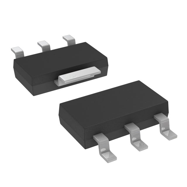
| 描述 | IC REG LDO 5V 0.15A SOT223低压差稳压器 5V/150MA LDO |
| 产品分类 | |
| 品牌 | ON Semiconductor |
| 产品手册 | |
| 产品图片 |
|
| rohs | 符合RoHS无铅 / 符合限制有害物质指令(RoHS)规范要求 |
| 产品系列 | 电源管理 IC,低压差稳压器,ON Semiconductor NCV4266ST50T3G- |
| 数据手册 | |
| 产品型号 | NCV4266ST50T3G |
| 产品种类 | 低压差稳压器 |
| 供应商器件封装 | SOT-223 |
| 其它名称 | NCV4266ST50T3GOSDKR |
| 包装 | Digi-Reel® |
| 商标 | ON Semiconductor |
| 回动电压—最大值 | 500 mV |
| 安装类型 | 表面贴装 |
| 安装风格 | SMD/SMT |
| 封装 | Reel |
| 封装/外壳 | TO-261-4,TO-261AA |
| 封装/箱体 | SOT-223 |
| 工作温度 | -40°C ~ 150°C |
| 工厂包装数量 | 4000 |
| 最大输入电压 | 45 V |
| 标准包装 | 1 |
| 电压-跌落(典型值) | 0.25V @ 150mA |
| 电压-输入 | 最高 45 V |
| 电压-输出 | 5V |
| 电流-输出 | 150mA |
| 电流-限制(最小值) | 150mA |
| 稳压器拓扑 | 正,固定式 |
| 稳压器数 | 1 |
| 系列 | NCV4266 |
| 负载调节 | 3 mV |
| 输出电压 | 5 V |
| 输出电流 | 150 mA |


- 商务部:美国ITC正式对集成电路等产品启动337调查
- 曝三星4nm工艺存在良率问题 高通将骁龙8 Gen1或转产台积电
- 太阳诱电将投资9.5亿元在常州建新厂生产MLCC 预计2023年完工
- 英特尔发布欧洲新工厂建设计划 深化IDM 2.0 战略
- 台积电先进制程称霸业界 有大客户加持明年业绩稳了
- 达到5530亿美元!SIA预计今年全球半导体销售额将创下新高
- 英特尔拟将自动驾驶子公司Mobileye上市 估值或超500亿美元
- 三星加码芯片和SET,合并消费电子和移动部门,撤换高东真等 CEO
- 三星电子宣布重大人事变动 还合并消费电子和移动部门
- 海关总署:前11个月进口集成电路产品价值2.52万亿元 增长14.8%


PDF Datasheet 数据手册内容提取
NCV4266 Regulator with Enable, 150 mA, Low-Dropout Voltage The NCV4266 is a 150 mA output current integrated low dropout regulator family designed for use in harsh automotive environments. www.onsemi.com It includes wide operating temperature and input voltage ranges. The device is offered with fixed voltage versions of 3.3 V and 5.0 V available in 2% output voltage accuracy. It has a high peak input voltage tolerance and reverse input voltage protection. It also provides overcurrent protection, overtemperature protection and SOT−223 enable function for control of the state of the output voltage. The ST SUFFIX NCV4266 is available in SOT−223 surface mount package. The CASE 318E output is stable over a wide output capacitance and ESR range. The NCV4266 has improved startup behavior during input voltage MARKING DIAGRAM transients. Features • 3.3 V and 5.0 V Output Voltage AYW • 4266x(cid:2) 150 mA Output Current (cid:2) • 500 mV (max) Dropout Voltage 1 • Enable Input • Very Low Current Consumption A = Assembly Location • Fault Protection Y = Year W = Work Week ♦ +45 V Peak Transient Voltage x = Voltage Option ♦ −42 V Reverse Voltage 3.3 V (x = 3) ♦ Short Circuit 5.0 V (x = 5) ♦ Thermal Overload (cid:2) = Pb−Free Package • NCV Prefix for Automotive and Other Applications Requiring (Note: Microdot may be in either location) Unique Site and Control Change Requirements; AEC−Q100 Qualified and PPAP Capable • These are Pb−Free Devices ORDERING INFORMATION See detailed ordering and shipping information in the ordering information section on page 10 of this data sheet. I Q Error Current Limit and Amplifier Saturation Sense Bandgap − Reference + Thermal Shutdown EN GND Figure 1. Block Diagram © Semiconductor Components Industries, LLC, 2012 1 Publication Order Number: November, 2018 − Rev. 3 NCV4266/D
NCV4266 PIN FUNCTION DESCRIPTION Pin No. Symbol Description 1 I Input; Battery Supply Input Voltage. 2 EN Enable Input; low level disables the IC. 3 Q Output; Bypass with a capacitor to GND. 4 GND Ground. MAXIMUM RATINGS* Rating Symbol Min Max Unit Input Voltage VI −42 45 V Input Peak Transient Voltage VI − 45 V Enable Input Voltage VEN −42 45 V Output Voltage VQ −1.0 40 V Ground Current Iq − 100 mA Input Voltage Operating Range VI VQ + 0.5 V or 40 V 4.5 (Note 1) ESD Susceptibility (Human Body Model) − 4.0 − kV (Machine Model) − 250 − V Junction Temperature TJ −40 150 °C Storage Temperature Tstg −50 150 °C Stresses exceeding those listed in the Maximum Ratings table may damage the device. If any of these limits are exceeded, device functionality should not be assumed, damage may occur and reliability may be affected. *During the voltage range which exceeds the maximum tested voltage of I, operation is assured, but not specified. Wider limits may apply. Thermal dissipation must be observed closely. 1. Minimum VI = 4.5 V or (VQ + 0.5 V), whichever is higher. LEAD TEMPERATURE SOLDERING REFLOW AND MSL (Note 2) Rating Symbol Min Max Unit Lead Temperature Soldering TSLD °C Reflow (SMD styles only), Leaded, 60−150 s above 183, 30 s max at peak − 240 Reflow (SMD styles only), Free, 60−150 s above 217, 40 s max at peak − 265 Wave Solder (through hole styles only), 12 sec max − 310 Moisture Sensitivity Level MSL 3 − 2. Per IPC / JEDEC J−STD−020C. THERMAL CHARACTERISTICS Characteristic Test Conditions (Typical Value) Unit Min Pad Board (Note 3) 1(cid:2) Pad Board (Note 4) Junction−to−Tab (psi−JL4, (cid:2)JL4) 15.7 18 C/W Junction−to−Ambient (R(cid:3)JA, (cid:3)JA) 96 77 C/W 3. 1 oz. copper, 0.26 inch2 (168 mm2) copper area, 0.062″ thick FR4. 4. 1 oz. copper, 1.14 inch2 (736 mm2) copper area, 0.062″ thick FR4. www.onsemi.com 2
NCV4266 ELECTRICAL CHARACTERISTICS (VI = 13.5 V; −40°C < TJ < 150°C; unless otherwise noted.) Characteristic Symbol Test Conditions Min Typ Max Unit OUTPUT Output Voltage (5.0 V Version) VQ 5.0 mA < IQ < 150 mA, 6 V < VI < 28 V 4.9 5.0 5.1 V Output Voltage (3.3 V Version) VQ 5.0 mA < IQ < 150 mA, 4.5 V < VI < 28 V 3.234 3.3 3.366 V Output Current Limitation IQ VQ = 90% VQTYP 150 200 500 mA Quiescent Current (Sleep Mode) Iq VEN = 0 V − − 10 (cid:4)A Iq = II − IQ Quiescent Current, Iq = II − IQ Iq IQ = 1.0 mA − 130 200 (cid:4)A Quiescent Current, Iq = II − IQ Iq IQ = 150 mA − 10 15 mA Dropout Voltage (5.0 V Version) VDR IQ = 150 mA, VDR = VI − VQ (Note 5) − 250 500 mV Load Regulation (cid:5)VQ,LO IQ = 5.0 mA to 150 mA − 3.0 20 mV Line Regulation (5.0 V Version) (cid:5)VQ (cid:5)VI = 6.0 V to 28 V, IQ = 5.0 mA − 10 25 mV Line Regulation (3.3 V Version) (cid:5)VQ (cid:5)VI = 4.5 V to 28 V, IQ = 5.0 mA − 10 25 mV Power Supply Ripple Rejection PSRR fr = 100 Hz, Vr = 0.5 VPP − 70 − dB Temperature Output Voltage Drift dVQ/dT − − 0.5 − mV/K ENABLE INPUT Enable Voltage, Output High VEN VQ (cid:2) VQMIN − 2.3 2.8 V Enable Voltage, Output Low (Off) VEN VQ (cid:3) 0.1 V 1.8 2.2 − V Enable Input Current IEN VEN = 5.0 V 5.0 10 20 (cid:4)A THERMAL SHUTDOWN Thermal Shutdown Temperature* TSD 150 − 210 °C *Guaranteed by design, not tested in production. 5. Measured when the output voltage VQ has dropped 100 mV from the nominal value obtained at V = 13.5 V. II I 1 3 Q IQ Output Input CI1 CI2 CQ 1.0 (cid:4)F 100 nF NCV4266 22 (cid:4)F EN 2 RL 4 IEN GND Figure 2. Applications Circuit www.onsemi.com 3
NCV4266 TYPICAL PERFORMANCE CHARACTERISTICS 100 Unstable Region CQ = 10 (cid:4)F − 100 (cid:4)F 10 (cid:6)) R ( 1 S E Stable Region 0.1 0.01 0 25 50 75 100 125 150 OUTPUT CURRENT (mA) Figure 3. Output Stability with Output Capacitor ESR 5.2 3.5 VI = 13.5 V VI = 13.5 V V) RL = 1 k(cid:6) V) RL = 660 (cid:6) E ( 5.1 E ( 3.4 G G A A T T L L O O V V T 5.0 T 3.3 U U P P T T U U O O , Q 4.9 , Q 3.2 V V 4.8 3.1 −40 0 40 80 120 160 −40 0 40 80 120 160 TJ, JUNCTION TEMPERATURE (°C) TJ, JUNCTION TEMPERATURE (°C) Figure 4. Output Voltage vs. Junction Figure 5. Output Voltage vs. Junction Temperature, 5.0 V Version Temperature, 3.3 V Version 25 6 TJ = 25°C TJ = 25°C mA) RL = 33 (cid:6) mA) 5 RL = 22 (cid:6) T ( 20 T ( N N E E R R 4 R 15 R U U C C T T 3 N N E 10 E C C S S 2 E E UI UI Q 5 Q , q , q 1 I I 0 0 0 5 10 15 20 25 30 35 40 0 5 10 15 20 25 30 35 40 VI, INPUT VOLTAGE (V) VI, INPUT VOLTAGE (V) Figure 6. Quiescent Current vs. Input Voltage, Figure 7. Quiescent Current vs. Input Voltage, 5.0 V Version 3.3 V Version www.onsemi.com 4
NCV4266 TYPICAL PERFORMANCE CHARACTERISTICS 6 6 TJ = 25°C TJ = 25°C E (V) 5 RL = 33 (cid:6) E (V) 5 RL = 22 (cid:6) G G A A T 4 T 4 L L O O V V T 3 T 3 U U P P T T U U O 2 O 2 , Q , Q V V 1 1 0 0 0 2 4 6 8 10 0 2 4 6 8 10 VI, INPUT VOLTAGE (V) VI, INPUT VOLTAGE (V) Figure 8. Output Voltage vs. Input Voltage, Figure 9. Output Voltage vs. Input Voltage, 5.0 V Version 3.3 V Version 6.0 1 4.0 0 A) A) m 2.0 m −1 T ( T ( N 0 N −2 E E R R R −2.0 R −3 U U C C T −4.0 T −4 U U P P I, INI −−86..00 TJ = 25°C I, INI −−65 TJ = 25°C RL = 6.8 k(cid:6) RL = 6.8 k(cid:6) −10 −7 −50 −25 0 25 50 −50 −25 0 25 50 VI, INPUT VOLTAGE (V) VI, INPUT VOLTAGE (V) Figure 10. Input Current vs. Input Voltage, Figure 11. Input Current vs. Input Voltage, 5.0 V Version 3.3 V Version 300 400 GE (mV) 250 T (mA) 330500 TVJQ = = 2 05 °VC OLTA 200 TJ = 125°C RREN 250 V U UT 150 T C 200 PO TJ = 25°C PU O T 150 R 100 U D O , R , Q 100 D 50 I V 50 0 0 0 25 50 75 100 125 150 0 5 10 15 20 25 30 35 40 IQ, OUTPUT CURRENT (mA) VI, INPUT VOLTAGE (V) Figure 12. Dropout Voltage vs. Output Current Figure 13. Maximum Output Current vs. (5.0 V Version only) Input Voltage www.onsemi.com 5
NCV4266 TYPICAL PERFORMANCE CHARACTERISTICS 1 6 TJ = 25°C TJ = 25°C mA) VI = 13.5 V mA) 5 VI = 13.5 V T ( 0.8 T ( N N E E 4 R R R 0.6 R U U T C T C 3 N N E 0.4 E SC SC 2 E E UI UI I, Qq 0.2 I, Qq 1 0 0 0 5 10 15 20 25 30 0 25 50 75 100 125 150 IQ, OUTPUT CURRENT (mA) IQ, OUTPUT CURRENT (mA) Figure 14. Quiescent Current vs. Output Current Figure 15. Quiescent Current vs. Output (Low Load), 5.0 V Version Current (High Load), 5.0 V Version 1 6 TJ = 25°C TJ = 25°C mA) VI = 13.5 V mA) 5 VI = 13.5 V T ( 0.8 T ( N N E E 4 R R R 0.6 R U U T C T C 3 N N E 0.4 E SC SC 2 E E UI UI I, Qq 0.2 I, Qq 1 0 0 0 5 10 15 20 25 30 0 25 50 75 100 125 150 IQ, OUTPUT CURRENT (mA) IQ, OUTPUT CURRENT (mA) Figure 16. Quiescent Current vs. Output Current Figure 17. Quiescent Current vs. Output (Low Load), 3.3 V Version Current (High Load), 3.3 V Version www.onsemi.com 6
NCV4266 Circuit Description transient response and loop stability. The capacitor value The NCV4266 is an integrated low dropout regulator that and type should be based on cost, availability, size and provides a regulated voltage at 150 mA to the output. It is temperature constraints. The aluminum electrolytic enabled with an input to the enable pin. The regulator capacitor is the least expensive solution, but, if the circuit voltage is provided by a PNP pass transistor controlled by operates at low temperatures (−25°C to −40°C), both the an error amplifier with a bandgap reference, which gives it value and ESR of the capacitor will vary considerably. The the lowest possible dropout voltage. The output current capacitor manufacturer’s data sheet usually provides this capability is 150 mA, and the base drive quiescent current information. is controlled to prevent oversaturation when the input The value for the output capacitor C , shown in Figure 2, Q voltage is low or when the output is overloaded. The should work for most applications; see also Figure 3 for regulator is protected by both current limit and thermal output stability at various load and Output Capacitor ESR shutdown. Thermal shutdown occurs above 150°C to conditions. Stable region of ESR in Figure 3 shows ESR protect the IC during overloads and extreme ambient values at which the LDO output voltage does not have any temperatures. permanent oscillations at any dynamic changes of output load current. Marginal ESR is the value at which the output Regulator voltage waving is fully damped during four periods after The error amplifier compares the reference voltage to a the load change and no oscillation is further observable. sample of the output voltage (VQ) and drives the base of a ESR characteristics were measured with ceramic PNP series pass transistor via a buffer. The reference is a capacitors and additional series resistors to emulate ESR. bandgap design to give it a temperature−stable output. Low duty cycle pulse load current technique has been used Saturation control of the PNP is a function of the load to maintain junction temperature close to ambient current and input voltage. Oversaturation of the output temperature. power device is prevented, and quiescent current in the ground pin is minimized. See Figure 2, Test Circuit, for Enable Input circuit element nomenclature illustration. The enable pin is used to turn the regulator on or off. By holding the pin down to a voltage less than 1.8 V, the output Regulator Stability Considerations of the regulator will be turned off. When the voltage on the The input capacitors (CI1 and CI2) are necessary to enable pin is greater than 2.8 V, the output of the regulator stabilize the input impedance to avoid voltage line will be enabled to power its output to the regulated output influences. Using a resistor of approximately 1.0 (cid:6) in voltage. The enable pin may be connected directly to the series with C can stop potential oscillations caused by I2 input pin to give constant enable to the output regulator. stray inductance and capacitance. The output capacitor helps determine three main characteristics of a linear regulator: startup delay, load www.onsemi.com 7
NCV4266 Calculating Power Dissipation Heatsinks in a Single Output Linear Regulator A heatsink effectively increases the surface area of the The maximum power dissipation for a single output package to improve the flow of heat away from the IC and regulator (Figure 18) is: into the surrounding air. PD(max)(cid:4)[VI(max)(cid:5)VQ(min)]IQ(max) (1) Each material in the heat flow path between the IC and the outside environment will have a thermal resistance. (cid:6)VI(max)Iq Like series electrical resistances, these resistances are where summed to determine the value of R(cid:3)JA: VI(max) is the maximum input voltage, R(cid:3)JA(cid:4)R(cid:3)JC(cid:6)R(cid:3)CS(cid:6)R(cid:3)SA (3) V is the minimum output voltage, Q(min) where I is the maximum output current for the Q(max) application, R(cid:3)JC is the junction−to−case thermal resistance, I is the quiescent current the regulator R(cid:3)CS is the case−to−heatsink thermal resistance, q consumes at I . R(cid:3)SA is the heatsink−to−ambient thermal Q(max) resistance. Once the value of P is known, the maximum D(max) permissible value of R(cid:3)JA can be calculated: R(cid:3)JC appears in the package section of the data sheet. R(cid:3)JA(cid:4)150oPCD(cid:5)TA (2) LRi(cid:3)kSeA Ra(cid:3)reJA f,u int cttoioon iss oaf ftuhnec tpioacnk oafg ep atcykpaeg, eh etyaptsei.n kR (cid:3)aCnSd atnhde interface between them. These values appear in data sheets The value of R(cid:3)JA can then be compared with those in the of heatsink manufacturers. package section of the data sheet. Those packages with Thermal, mounting, and heatsinking considerations are R(cid:3)JA less than the calculated value in Equation 2 will keep the die temperature below 150°C. discussed in the ON Semiconductor application note AN1040/D. In some cases, none of the packages will be sufficient to dissipate the heat generated by the IC, and an external heatsink will be required. II IQ VI SMART VQ REGULATOR® }Control Features Iq Figure 18. Single Output Regulator with Key Performance Parameters Labeled www.onsemi.com 8
NCV4266 140 W) °/ 130 C E ( C 120 N A T 110 S SI E 100 R L A 90 M 1 oz R E 80 H T , A 70 (cid:3)J 2 oz R 60 0 100 200 300 400 500 600 700 COPPER HEAT SPREADER AREA (mm2) Figure 19. R(cid:2)JA vs. Copper Spreader Area 100 Cu Area 167 mm2 Cu Area 736 mm2 10 W °/ C R(t) 1 0.1 0.000001 0.00001 0.0001 0.001 0.01 0.1 1 10 100 1000 TIME (sec) Figure 20. Single−Pulse Heating Curves 100 50% Duty Cycle 20% W °C/10 10% 2 m 5% m 36 2% 7 JA 1 1% (cid:3) R Non−normalized Response 0.1 0.000001 0.00001 0.0001 0.001 0.01 0.1 1 10 100 1000 PULSE WIDTH (sec) Figure 21. Duty Cycle for 1(cid:2) Spreader Boards www.onsemi.com 9
NCV4266 ORDERING INFORMATION Device* Output Voltage Package Shipping† NCV4266ST33T3G 3.3 V SOT−223 4000 / Tape & Reel (Pb−Free) NCV4266ST50T3G 5.0 V SOT−223 4000 / Tape & Reel (Pb−Free) †For information on tape and reel specifications, including part orientation and tape sizes, please refer to our Tape and Reel Packaging Specifications Brochure, BRD8011/D. *NCV Prefix for Automotive and Other Applications Requiring Unique Site and Control Change Requirements; AEC−Q100 Qualified and PPAP Capable. www.onsemi.com 10
MECHANICAL CASE OUTLINE PACKAGE DIMENSIONS SOT−223 (TO−261) CASE 318E−04 ISSUE R SCALE 1:1 DATE 02 OCT 2018 (cid:2) (cid:2) Electronic versions are uncontrolled except when accessed directly from the Document Repository. DOCUMENT NUMBER: 98ASB42680B Printed versions are uncontrolled except when stamped “CONTROLLED COPY” in red. DESCRIPTION: SOT−223 (TO−261) PAGE 1 OF 2 ON Semiconductor and are trademarks of Semiconductor Components Industries, LLC dba ON Semiconductor or its subsidiaries in the United States and/or other countries. ON Semiconductor reserves the right to make changes without further notice to any products herein. ON Semiconductor makes no warranty, representation or guarantee regarding the suitability of its products for any particular purpose, nor does ON Semiconductor assume any liability arising out of the application or use of any product or circuit, and specifically disclaims any and all liability, including without limitation special, consequential or incidental damages. ON Semiconductor does not convey any license under its patent rights nor the rights of others. © Semiconductor Components Industries, LLC, 2018 www.onsemi.com
SOT−223 (TO−261) CASE 318E−04 ISSUE R DATE 02 OCT 2018 STYLE 1: STYLE 2: STYLE 3: STYLE 4: STYLE 5: PIN 1.BASE PIN 1.ANODE PIN 1.GATE PIN 1.SOURCE PIN 1.DRAIN 2.COLLECTOR 2.CATHODE 2.DRAIN 2.DRAIN 2.GATE 3.EMITTER 3.NC 3.SOURCE 3.GATE 3.SOURCE 4.COLLECTOR 4.CATHODE 4.DRAIN 4.DRAIN 4.GATE STYLE 6: STYLE 7: STYLE 8: STYLE 9: STYLE 10: PIN 1.RETURN PIN 1.ANODE 1 CANCELLED PIN 1.INPUT PIN 1.CATHODE 2.INPUT 2.CATHODE 2.GROUND 2.ANODE 3.OUTPUT 3.ANODE 2 3.LOGIC 3.GATE 4.INPUT 4.CATHODE 4.GROUND 4.ANODE STYLE 11: STYLE 12: STYLE 13: PIN 1.MT 1 PIN 1.INPUT PIN 1.GATE 2.MT 2 2.OUTPUT 2.COLLECTOR 3.GATE 3.NC 3.EMITTER 4.MT 2 4.OUTPUT 4.COLLECTOR GENERIC MARKING DIAGRAM* AYW XXXXX(cid:2) (cid:2) 1 A = Assembly Location Y = Year W = Work Week XXXXX = Specific Device Code (cid:2) = Pb−Free Package (Note: Microdot may be in either location) *This information is generic. Please refer to device data sheet for actual part marking. Pb−Free indicator, “G” or microdot “(cid:2)”, may or may not be present. Some products may not follow the Generic Marking. Electronic versions are uncontrolled except when accessed directly from the Document Repository. DOCUMENT NUMBER: 98ASB42680B Printed versions are uncontrolled except when stamped “CONTROLLED COPY” in red. DESCRIPTION: SOT−223 (TO−261) PAGE 2 OF 2 ON Semiconductor and are trademarks of Semiconductor Components Industries, LLC dba ON Semiconductor or its subsidiaries in the United States and/or other countries. ON Semiconductor reserves the right to make changes without further notice to any products herein. ON Semiconductor makes no warranty, representation or guarantee regarding the suitability of its products for any particular purpose, nor does ON Semiconductor assume any liability arising out of the application or use of any product or circuit, and specifically disclaims any and all liability, including without limitation special, consequential or incidental damages. ON Semiconductor does not convey any license under its patent rights nor the rights of others. © Semiconductor Components Industries, LLC, 2018 www.onsemi.com
ON Semiconductor and are trademarks of Semiconductor Components Industries, LLC dba ON Semiconductor or its subsidiaries in the United States and/or other countries. ON Semiconductor owns the rights to a number of patents, trademarks, copyrights, trade secrets, and other intellectual property. A listing of ON Semiconductor’s product/patent coverage may be accessed at www.onsemi.com/site/pdf/Patent−Marking.pdf. ON Semiconductor reserves the right to make changes without further notice to any products herein. ON Semiconductor makes no warranty, representation or guarantee regarding the suitability of its products for any particular purpose, nor does ON Semiconductor assume any liability arising out of the application or use of any product or circuit, and specifically disclaims any and all liability, including without limitation special, consequential or incidental damages. Buyer is responsible for its products and applications using ON Semiconductor products, including compliance with all laws, regulations and safety requirements or standards, regardless of any support or applications information provided by ON Semiconductor. “Typical” parameters which may be provided in ON Semiconductor data sheets and/or specifications can and do vary in different applications and actual performance may vary over time. All operating parameters, including “Typicals” must be validated for each customer application by customer’s technical experts. ON Semiconductor does not convey any license under its patent rights nor the rights of others. ON Semiconductor products are not designed, intended, or authorized for use as a critical component in life support systems or any FDA Class 3 medical devices or medical devices with a same or similar classification in a foreign jurisdiction or any devices intended for implantation in the human body. Should Buyer purchase or use ON Semiconductor products for any such unintended or unauthorized application, Buyer shall indemnify and hold ON Semiconductor and its officers, employees, subsidiaries, affiliates, and distributors harmless against all claims, costs, damages, and expenses, and reasonable attorney fees arising out of, directly or indirectly, any claim of personal injury or death associated with such unintended or unauthorized use, even if such claim alleges that ON Semiconductor was negligent regarding the design or manufacture of the part. ON Semiconductor is an Equal Opportunity/Affirmative Action Employer. This literature is subject to all applicable copyright laws and is not for resale in any manner. PUBLICATION ORDERING INFORMATION LITERATURE FULFILLMENT: N. American Technical Support: 800−282−9855 Toll Free ON Semiconductor Website: www.onsemi.com Literature Distribution Center for ON Semiconductor USA/Canada 19521 E. 32nd Pkwy, Aurora, Colorado 80011 USA Europe, Middle East and Africa Technical Support: Order Literature: http://www.onsemi.com/orderlit Phone: 303−675−2175 or 800−344−3860 Toll Free USA/Canada Phone: 421 33 790 2910 Fax: 303−675−2176 or 800−344−3867 Toll Free USA/Canada For additional information, please contact your local Email: orderlit@onsemi.com Sales Representative ◊
Mouser Electronics Authorized Distributor Click to View Pricing, Inventory, Delivery & Lifecycle Information: O N Semiconductor: NCV4266ST50T3G NCV4266ST33T3G