ICGOO在线商城 > 集成电路(IC) > PMIC - 稳压器 - 线性 > TPS74201KTWT
 Datasheet下载
- 型号: TPS74201KTWT
- 制造商: Texas Instruments
- 库位|库存: xxxx|xxxx
- 要求:
| 数量阶梯 | 香港交货 | 国内含税 |
| +xxxx | $xxxx | ¥xxxx |
查看当月历史价格
查看今年历史价格
TPS74201KTWT产品简介:
ICGOO电子元器件商城为您提供TPS74201KTWT由Texas Instruments设计生产,在icgoo商城现货销售,并且可以通过原厂、代理商等渠道进行代购。 TPS74201KTWT价格参考¥29.40-¥45.97。Texas InstrumentsTPS74201KTWT封装/规格:PMIC - 稳压器 - 线性, Linear Voltage Regulator IC Positive Adjustable 1 Output 0.8 V ~ 3.6 V 1.5A DDPAK/TO-263-7。您可以下载TPS74201KTWT参考资料、Datasheet数据手册功能说明书,资料中有TPS74201KTWT 详细功能的应用电路图电压和使用方法及教程。
TPS74201KTWT 是由德州仪器(Texas Instruments)生产的一款线性稳压器(PMIC - Power Management IC),属于低功耗、低压差(LDO)稳压器系列。以下是其主要应用场景:

1. 便携式电子设备:
   TPS74201KTWT 的低静态电流(典型值为 16 µA)和高电源抑制比(PSRR)使其非常适合用于电池供电的便携式设备,例如智能手机、平板电脑、可穿戴设备和手持式医疗设备。这些设备对功耗敏感,需要高效且稳定的电源管理。

2. 无线通信模块:
   该器件支持 1.8V 至 5.5V 的输入电压范围,并能提供高达 300mA 的输出电流,适用于为无线通信模块(如蓝牙、Wi-Fi 和 Zigbee 模块)供电。其出色的噪声性能和稳定性有助于提高射频信号的质量。

3. 传感器系统:
   在物联网(IoT)应用中,TPS74201KTWT 可以为各种传感器(如温度、压力、加速度传感器)提供稳定且低噪声的电源。其小封装尺寸(WSON-8 封装)和高效性能使其非常适合紧凑型设计。

4. 嵌入式系统:
   该稳压器适用于嵌入式系统的电源管理,例如微控制器(MCU)、数字信号处理器(DSP)和其他低功耗逻辑电路的供电。其快速瞬态响应能力能够满足这些设备在动态负载条件下的需求。

5. 工业自动化:
   在工业环境中,TPS74201KTWT 可用于为现场总线模块、数据采集系统和远程监控设备供电。其宽输入电压范围和过流保护功能增强了其在复杂工业环境中的可靠性。

6. 消费类电子产品:
   包括数码相机、便携式音频设备和电子阅读器在内的消费类电子产品也可以使用 TPS74201KTWT,以实现高效的电源管理和延长电池寿命。

总结来说,TPS74201KTWT 凭借其低功耗、高稳定性和紧凑的设计,广泛应用于需要高效电源管理的各种场景,特别是在对功耗和空间要求严格的便携式和嵌入式设备中表现优异。
| 参数 | 数值 |
| 产品目录 | 集成电路 (IC)半导体 |
| 描述 | IC REG LDO ADJ 1.5A 7DDPAK低压差稳压器 Sgl Output LDO 1.5A Adj 0.8 to 3.3V |
| DevelopmentKit | TPS74201EVM-118 |
| 产品分类 | |
| 品牌 | Texas Instruments |
| 产品手册 | |
| 产品图片 |
|
| rohs | 符合RoHS无铅 / 符合限制有害物质指令(RoHS)规范要求 |
| 产品系列 | 电源管理 IC,低压差稳压器,Texas Instruments TPS74201KTWT- |
| 数据手册 | |
| 产品型号 | TPS74201KTWT |
| 产品目录页面 | |
| 产品种类 | Regulators - Low Dropout (LDO) |
| 供应商器件封装 | DDPAK/TO-263-7 |
| 其它名称 | 296-21505-2 |
| 制造商产品页 | http://www.ti.com/general/docs/suppproductinfo.tsp?distId=10&orderablePartNumber=TPS74201KTWT |
| 包装 | 带卷 (TR) |
| 参考电压 | 0.804 V |
| 商标 | Texas Instruments |
| 回动电压—最大值 | 120 mV at 1.5 A |
| 安装类型 | 表面贴装 |
| 安装风格 | SMD/SMT |
| 封装 | Reel |
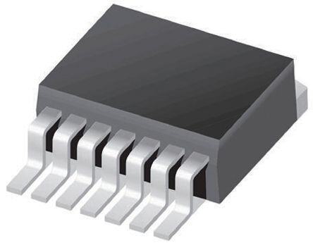
| 封装/外壳 | TO-263-8,D²Pak(7 引线+接片),TO-263CA |
| 封装/箱体 | TO-263-7 |
| 工作温度 | -40°C ~ 125°C |
| 工厂包装数量 | 50 |
| 最大功率耗散 | 5.32 W |
| 最大工作温度 | + 125 C |
| 最大输入电压 | 5.5 V |
| 最小工作温度 | - 40 C |
| 最小输入电压 | + 0.8 V |
| 标准包装 | 50 |
| 电压-跌落(典型值) | 0.06V @ 1.5A |
| 电压-输入 | 0.86 V ~ 5.5 V |
| 电压-输出 | 0.8 V ~ 3.6 V |
| 电压调节准确度 | 1 % |
| 电流-输出 | 1.5A |
| 电流-限制(最小值) | 1.8A |
| 稳压器拓扑 | 正,可调式 |
| 稳压器数 | 1 |
| 系列 | TPS74201 |
| 线路调整率 | 0.0005 % / V |
| 负载调节 | 0.04 % / A |
| 输出电压 | 796 mV to 3.6 V |
| 输出电流 | 1.5 A |
| 输出端数量 | 1 Output |
| 输出类型 | Adjustable |
| 配用 | /product-detail/zh/TPS74201EVM-118/296-31430-ND/1673007 |


- 商务部:美国ITC正式对集成电路等产品启动337调查
- 曝三星4nm工艺存在良率问题 高通将骁龙8 Gen1或转产台积电
- 太阳诱电将投资9.5亿元在常州建新厂生产MLCC 预计2023年完工
- 英特尔发布欧洲新工厂建设计划 深化IDM 2.0 战略
- 台积电先进制程称霸业界 有大客户加持明年业绩稳了
- 达到5530亿美元!SIA预计今年全球半导体销售额将创下新高
- 英特尔拟将自动驾驶子公司Mobileye上市 估值或超500亿美元
- 三星加码芯片和SET,合并消费电子和移动部门,撤换高东真等 CEO
- 三星电子宣布重大人事变动 还合并消费电子和移动部门
- 海关总署:前11个月进口集成电路产品价值2.52万亿元 增长14.8%


PDF Datasheet 数据手册内容提取
Product Order Technical Tools & Support & Folder Now Documents Software Community TPS74201 SBVS064N–DECEMBER2005–REVISEDNOVEMBER2016 TPS742 1.5-A Ultra-LDO With Programmable Soft-Start 1 Features 3 Description • InputVoltageRange:0.8Vto5.5V The TPS742 series of low-dropout (LDO) linear 1 regulators provide an easy-to-use, robust power- • Soft-Start(SS)PinProvidesaLinearStart-Up management solution for a wide variety of WithRampTimeSetbyExternalCapacitor applications. User-programmable soft-start minimizes • 1%AccuracyOverLine,Load,andTemperature stress on the input power source by reducing • SupportsInputVoltagesasLowas0.8VWith capacitive inrush current on start-up. The soft-start is monotonic and well suited for powering many ExternalBiasSupply different types of processors and ASICs. The enable • AdjustableOutput(0.8Vto3.6V) input and power-good output allow easy sequencing • Ultra-LowDropout:55mVat1.5A(Typical) with external regulators. This complete flexibility • StableWithAnyorNoOutputCapacitor permits the user to configure a solution that meets the sequencing requirements of FPGAs, DSPs, and • ExcellentTransientResponse otherapplicationswithspecialstart-uprequirements. • Open-DrainPower-Good(VQFN) A precision reference and error amplifier deliver 1% • ActiveHighEnable accuracy over load, line, temperature, and process. Each LDO is stable with low-cost ceramic output 2 Applications capacitors, and the family is fully specified from • FPGAApplications –40°C to 125°C. The TPS742 devices are offered in a small 5-mm × 5-mm VQFN (RGW) and a small • DSPCoreandI/OVoltages 3.5-mm × 3.5-mm VQFN (RGR) package, yielding a • Servers highly compact total solution size. For applications • Post-RegulationApplications that require additional power dissipation, the DDPAK/TO-263(KTW)packageisalsoavailable. • ApplicationsWithSpecialStart-UpTimeor SequencingRequirements DeviceInformation(1) PART PACKAGE BODYSIZE(NOM) NUMBER VQFN(20),RGW 5.00mm×5.00mm TPS74201 VQFN(20),RGR 3.50mm×3.50mm DDPAK/TO-263(7) 8.89mm×10.10mm (1) For all available packages, see the orderable addendum at theendofthedatasheet. TypicalApplicationAdjustableOutputVersion TurnonResponse VIN IN PG C1µINF BIAS R3 EN TPS74201 OUT VOUT VBIAS C1µBFIAS SS GND FB R1 COUT CSSC=S S0=m F0.001mF VOUT CSS R2 1V/div CSS= 0.0047mF Optional 1.2V V EN 1V/div 0V Time (1ms/div) 1 An IMPORTANT NOTICE at the end of this data sheet addresses availability, warranty, changes, use in safety-critical applications, intellectualpropertymattersandotherimportantdisclaimers.PRODUCTIONDATA.
TPS74201 SBVS064N–DECEMBER2005–REVISEDNOVEMBER2016 www.ti.com Table of Contents 1 Features.................................................................. 1 8.1 ApplicationInformation............................................15 2 Applications........................................................... 1 8.2 TypicalApplications................................................19 3 Description............................................................. 1 9 PowerSupplyRecommendations...................... 20 4 RevisionHistory..................................................... 2 10 Layout................................................................... 21 5 PinConfigurationandFunctions......................... 4 10.1 LayoutGuidelines.................................................21 10.2 LayoutExample....................................................21 6 Specifications......................................................... 5 10.3 ThermalProtection................................................22 6.1 AbsoluteMaximumRatings .....................................5 10.4 ThermalConsiderations........................................22 6.2 ESDRatings ............................................................5 11 DeviceandDocumentationSupport................. 25 6.3 RecommendedOperatingConditions.......................5 6.4 ThermalInformation..................................................6 11.1 DeviceSupport......................................................25 6.5 ElectricalCharacteristics...........................................7 11.2 DocumentationSupport .......................................25 6.6 TypicalCharacteristics..............................................8 11.3 ReceivingNotificationofDocumentationUpdates25 11.4 CommunityResources..........................................25 7 DetailedDescription............................................ 12 11.5 Trademarks...........................................................25 7.1 Overview.................................................................12 11.6 ElectrostaticDischargeCaution............................25 7.2 FunctionalBlockDiagram.......................................12 11.7 Glossary................................................................25 7.3 FeatureDescription.................................................13 12 Mechanical,Packaging,andOrderable 7.4 DeviceFunctionalModes........................................13 Information........................................................... 26 8 ApplicationandImplementation........................ 15 4 Revision History NOTE:Pagenumbersforpreviousrevisionsmaydifferfrompagenumbersinthecurrentversion. ChangesfromRevisionM(October2015)toRevisionN Page • AddedRGRpackagetodocument........................................................................................................................................ 1 • DeletedPackagesFeaturesbullet......................................................................................................................................... 1 • ChangedPower-GoodFeaturesbullet................................................................................................................................... 1 • AddedRGRpackagetolastparagraphofDescriptionsection ............................................................................................. 1 • AddedRGRrowtoDeviceInformationtable ........................................................................................................................ 1 • AddedRGRpackagetoPinConfigurationandFunctionssection........................................................................................ 4 • ChangedpinoutviewofKTWpackagetoTopView.............................................................................................................. 4 • AddedRGRpackagetoThermalInformationtable .............................................................................................................. 6 • ChangedFigure32titletoreflectbothVQFNpackagesinsteadofjustone....................................................................... 21 ChangesfromRevisionL(November2010)toRevisionM Page • AddedESDRatingstable,FeatureDescriptionsection,DeviceFunctionalModes,ApplicationandImplementation section,PowerSupplyRecommendationssection,Layoutsection,DeviceandDocumentationSupportsection,and Mechanical,Packaging,andOrderableInformationsection.................................................................................................. 1 • UpdatedthevalueinNormalandDropoutmodesunderV column............................................................................... 14 BIAS ChangesfromRevisionK(August,2010)toRevisionL Page • ReplacedtheDissipationRatingstablewiththeThermalInformationtable.......................................................................... 6 • CorrectedequationforTable2............................................................................................................................................. 17 • RevisedLayoutRecommendationsandPowerDissipationsection.................................................................................... 21 2 SubmitDocumentationFeedback Copyright©2005–2016,TexasInstrumentsIncorporated ProductFolderLinks:TPS74201
TPS74201 www.ti.com SBVS064N–DECEMBER2005–REVISEDNOVEMBER2016 ChangesfromRevisionJ(December,2009)toRevisionK Page • RevisedLayoutGuidelinessection...................................................................................................................................... 21 • ChangedfinalparagraphofLayoutGuidelinessection........................................................................................................ 21 • RevisedEstimatingJunctionTemperaturesection.............................................................................................................. 22 Copyright©2005–2016,TexasInstrumentsIncorporated SubmitDocumentationFeedback 3 ProductFolderLinks:TPS74201
TPS74201 SBVS064N–DECEMBER2005–REVISEDNOVEMBER2016 www.ti.com 5 Pin Configuration and Functions RGW,RGRPackages KTWPackage 20-PinVQFNwithExposedThermalPad 7-PinDDPAK/TO-263 TopView TopView T C C C U N N N N O I 5 4 3 2 1 IN 6 20 OUT IN 7 19 OUT 1 2 3 4 5 6 7 IN 8 TPS742xx 18 OUT GND PG 9 17 NC BIAS 10 16 FB/SNS SS OUT IN EN FB/ GND BIAS 1 2 3 4 5 SNS 1 1 1 1 1 N D C C S E N N N S G PinFunctions PIN KTW RGW,RGR I/O DESCRIPTION NAME (DDPAK/ (VQFN) TO-263) BIAS 6 10 I Biasinputvoltageforerroramplifier,reference,andinternalcontrolcircuits. Enablepin.Drivingthispinhighenablestheregulator.Drivingthispinlowputs EN 7 11 I theregulatorintoshutdownmode.Thispinmustnotbeleftfloating. Thispinisthefeedbackconnectiontothecentertapofanexternalresistor FB 2 16 I dividernetworkthatsetstheoutputvoltage.Thispinmustnotbeleftfloating. (Adjustableversiononly.) GND 4 12 — Ground IN 5 5,6,7,8 I Unregulatedinputtothedevice. 2,3,4, Noconnection.ThispincanbeleftfloatingorconnectedtoGNDtoallowbetter NC — O 13,14,17 thermalcontacttothetop-sideplane. OUT 3 1,18,19,20 O Regulatedoutputvoltage.Nocapacitorisrequiredonthispinforstability. PAD/TAB — — — Soldertothegroundplaneforincreasedthermalperformance. Power-Good(PG)isanopen-drain,active-highoutputthatindicatesthestatus ofV .WhenV exceedsthePGtripthreshold,thePGpingoesintoa OUT OUT high-impedancestate.WhenV isbelowthisthresholdthepinisdriventoa OUT PG — 9 O low-impedancestate.Connectapullupresistorfrom10kΩto1MΩfromthis pintoasupplyupto5.5V.Thesupplycanbehigherthantheinputvoltage. Alternatively,thePGpincanbeleftfloatingifoutputmonitoringisnot necessary. Thispinisthesenseconnectiontotheloaddevice.Thispinmustbe SNS 2 16 I connectedtoV andmustnotbeleftfloating.(Fixedversionsonly.) OUT Soft-Startpin.Acapacitorconnectedonthispintogroundsetsthestart-up SS 1 15 — time.Ifthispinisleftfloating,theregulatoroutputsoft-startramptimeis typically100μs. 4 SubmitDocumentationFeedback Copyright©2005–2016,TexasInstrumentsIncorporated ProductFolderLinks:TPS74201
TPS74201 www.ti.com SBVS064N–DECEMBER2005–REVISEDNOVEMBER2016 6 Specifications 6.1 Absolute Maximum Ratings atT =–40°Cto125°C(unlessotherwisenoted);allvoltagesarewithrespecttoGND(1) J MIN MAX UNIT V ,V Inputvoltage –0.3 6 V IN BIAS V Enablevoltage –0.3 6 V EN V Power-goodvoltage –0.3 6 V PG I PGsinkcurrent 0 1.5 mA PG V SSpinvoltage –0.3 6 V SS V Feedbackpinvoltage –0.3 6 V FB V Outputvoltage –0.3 V +0.3 V OUT IN I Maximumoutputcurrent Internallylimited OUT Outputshortcircuitduration Indefinite P Continuoustotalpowerdissipation SeeThermalInformation DISS T Operatingjunctiontemperature –40 125 °C J T Storagejunctiontemperature –55 150 °C stg (1) StressesbeyondthoselistedunderAbsoluteMaximumRatingsmaycausepermanentdamagetothedevice.Thesearestressratings only,whichdonotimplyfunctionaloperationofthedeviceattheseoranyotherconditionsbeyondthoseindicatedunderRecommended OperatingConditions.Exposuretoabsolute-maximum-ratedconditionsforextendedperiodsmayaffectdevicereliability. 6.2 ESD Ratings VALUE UNIT Humanbodymodel(HBM),perANSI/ESDA/JEDECJS-001(1) ±2000 V Electrostaticdischarge V (ESD) Chargeddevicemodel(CDM),perJEDECspecificationJESD22-C101(2) ±500 (1) JEDECdocumentJEP155statesthat500-VHBMallowssafemanufacturingwithastandardESDcontrolprocess. (2) JEDECdocumentJEP157statesthat250-VCDMallowssafemanufacturingwithastandardESDcontrolprocess. 6.3 Recommended Operating Conditions overoperatingfree-airtemperaturerange(unlessotherwisenoted) MIN NOM MAX UNIT V Inputsupplyvoltage V +V 5.5 V IN OUT DO V Enablesupplyvoltage 0 5.5 V EN V (1) BIASsupplyvoltage V +V (V ) 5.5 V BIAS OUT DO BIAS I Outputcurrent 0 1.5 A OUT C Outputcapacitor 0 µF OUT C (2) Inputcapacitor 1 µF IN C Biascapacitor 1 µF BIAS T Operatingjunctiontemperature –40 125 °C J (1) BIASsupplyisrequiredwhenV isbelowV +V (V ). IN OUT DO BIAS (2) IfV andV areconnectedtothesamesupply,therecommendedminimumcapacitorforthesupplyis4.7µF. IN BIAS Copyright©2005–2016,TexasInstrumentsIncorporated SubmitDocumentationFeedback 5 ProductFolderLinks:TPS74201
TPS74201 SBVS064N–DECEMBER2005–REVISEDNOVEMBER2016 www.ti.com 6.4 Thermal Information TPS742 THERMALMETRIC(1)(2)(3) RGW(VQFN) RGR(VQFN) KTW(DDPAK/TO- UNIT 263) 20PINS 20PINS 7PINS R Junction-to-ambientthermalresistance 35.4 39.1 26.6 °C/W θJA R Junction-to-case(top)thermalresistance 32.4 29.3 41.7 °C/W θJC(top) R Junction-to-boardthermalresistance 14.7 10.2 12.5 °C/W θJB ψ Junction-to-topcharacterizationparameter 0.4 0.4 4 °C/W JT ψ Junction-to-boardcharacterizationparameter 14.8 10.1 7.3 °C/W JB R Junction-to-case(bottom)thermalresistance 3.9 2.0 0.3 °C/W θJC(bot) (1) Formoreinformationabouttraditionalandnewthermalmetrics,seetheSemiconductorandICPackageThermalMetricsapplication report(SPRA953). (2) ForthermalestimatesofthisdevicebasedonPCBcopperarea,seetheTIPCBThermalCalculator. (3) ThermaldatafortheRGW,RGR,andKTWpackagesarederivedbythermalsimulationsbasedonJEDEC-standardmethodologyas specifiedintheJESD51series.Thefollowingassumptionsareusedinthesimulations: (a)i. RGW and RGR: The exposed pad is connected to the PCB ground layer through a 4 × 4 thermal via array. -ii.KTW:TheexposedpadisconnectedtothePCBgroundlayerthrougha6×6thermalviaarray. (b)Eachoftopandbottomcopperlayershasadedicatedpatternfor20%coppercoverage. (c) ThesedataweregeneratedwithonlyasingledeviceatthecenterofaJEDEChigh-K(2s2p)boardwith3in×3incopperarea.To understandtheeffectsofthecopperareaonthermalperformance,refertotheThermalConsiderationssection. 6 SubmitDocumentationFeedback Copyright©2005–2016,TexasInstrumentsIncorporated ProductFolderLinks:TPS74201
TPS74201 www.ti.com SBVS064N–DECEMBER2005–REVISEDNOVEMBER2016 6.5 Electrical Characteristics atV =1.1V,V =V +0.3V,C =C =0.1μF,C =10μF,I =50mA,V =5V,andT =–40°Cto125°C EN IN OUT IN BIAS OUT OUT BIAS J (unlessotherwisenoted);typicalvaluesareatT =25°C J PARAMETER TESTCONDITIONS MIN TYP MAX UNIT VIN Inputvoltage VOUT+VDO 5.5 V VBIAS Biaspinvoltage 2.375 5.25 V VREF Internalreference(adjustable) TJ=25°C 0.796 0.8 0.804 V Outputvoltage VIN=5V,IOUT=1.5A,VBIAS=5V VREF 3.6 V VOUT Accuracy(1) 2.375V≤VBIAS≤5.25V,VOUT+1.62V≤VBIAS –1% ±0.2% 1% 50mA≤IOUT≤1.5A VOUT(NOM)+0.3≤VIN≤5.5V,VQFN 0.0005 0.05 VOUT/VIN Lineregulation %/V VOUT(NOM)+0.3≤VIN≤5.5V,DDPAK/TO-263 0.0005 0.06 0mA≤IOUT≤50mA 0.013 %/mA VOUT/IOUT Loadregulation 50mA≤IOUT≤1.5A 0.04 %/A IOUT=1.5A,VBIAS–VOUT(NOM)≥1.62V,VQFN 55 100 VDO VINdropoutvoltage(2) IDODUTP=AK1/.T5OA-,2V6B3IAS–VOUT(NOM)≥1.62V, 60 120 mV VBIASdropoutvoltage(2) IOUT=1.5A,VIN=VBIAS 1.4 V ICL Currentlimit VOUT=80%×VOUT(NOM) 1.8 4 A IBIAS Biaspincurrent IOUT=0mAto1.5A 2 4 mA ISHDN Shutdownsupplycurrent(VIN) VEN≤0.4V 1 100 μA Feedback,Sensepin IFB,ISNS current(3) IOUT=50mAto1.5A –250 68 250 nA Power-supplyrejection 1kHz,IOUT=1.5A,VIN=1.8V,VOUT=1.5V 73 dB (VINtoVOUT) 300kHz,IOUT=1.5A,VIN=1.8V,VOUT=1.5V 42 PSRR Power-supplyrejection 1kHz,IOUT=1.5A,VIN=1.8V,VOUT=1.5V 62 dB (VBIAStoVOUT) 300kHz,IOUT=1.5A,VIN=1.8V,VOUT=1.5V 50 Noise Outputnoisevoltage 100Hzto100kHz,IOUT=1.5A,CSS=0.001μF 16×VOUT μVRMS VTRAN %traVnOsUieTndtroopduringload IOUT=50mAto1.5Aat1A/μs,COUT=none 3.5 %VOUT tSTR Minimumstart-uptime IOUT=1.5A,CSS=open 100 μs ISS Soft-startchargingcurrent VSS=0.4V 0.5 0.73 1 μA VEN,HI Enableinputhighlevel 1.1 5.5 V VEN,LO Enableinputlowlevel 0 0.4 V VEN,HYS Enablepinhysteresis 50 mV VEN,DG Enablepindeglitchtime 20 μs IEN Enablepincurrent VEN=5V 0.1 1 μA VIT PGtripthreshold VOUTdecreasing 86.5 90 93.5 %VOUT VHYS PGtriphysteresis 3 %VOUT VPG,LO PGoutputlowvoltage IPG=1mA(sinking),VOUT<VIT 0.3 V IPG,LKG PGleakagecurrent VPG=5.25V,VOUT>VIT 0.03 1 μA Operatingjunction TJ temperature –40 125 °C Thermalshutdown Shutdown,temperatureincreasing 155 TSD temperature Reset,temperaturedecreasing 140 °C (1) Adjustabledevicestestedat0.8V;resistortoleranceisnottakenintoaccount. (2) DropoutisdefinedasthevoltagefromtheinputtoV whenV is2%belownominal. OUT OUT (3) I ,I currentflowisoutofthedevice. FB SNS Copyright©2005–2016,TexasInstrumentsIncorporated SubmitDocumentationFeedback 7 ProductFolderLinks:TPS74201
TPS74201 SBVS064N–DECEMBER2005–REVISEDNOVEMBER2016 www.ti.com 6.6 Typical Characteristics atT =25°C,V =1.5V,V =V +0.3V,V =3.3V,I =50mA,EN=V ,C =1μF,C =4.7μF,C = J OUT IN OUT(TYP) BIAS OUT IN IN BIAS SS 0.01μF,andC =10μF(unlessotherwisenoted) OUT 1.0 0.050 0.9 Referred to IOUT= 50mA Referred to IOUT= 50mA 0.025 0.8 (%)UT 00..76 -40°C (%)UT -0.0250 +25°C VO 0.5 VO n n -0.050 hange i 00..43 +25°C hange i -0.075 -40°C +125°C C 0.2 C -0.100 0.1 +125°C -0.125 0 -0.1 -0.150 0 10 20 30 40 50 50 500 1000 1500 I (mA) I (mA) OUT OUT Figure1.LoadRegulation Figure2.LoadRegulation 0.05 100 0.04 0.03 n V(%)OUT 00..00210 TJ=-40°C oltage (mV) 7550 +125°C Change i --00..0012 TJ= +125°C TJ= +25°C Dropout V 25 +25°C -0.03 -40°C -0.04 -0.05 0 0 0.5 1.0 1.5 2.0 2.5 3.0 3.5 4.0 4.5 0 0.5 1.0 1.5 V -V (V) I (A) IN OUT OUT Figure3.LineRegulation Figure4.V DropoutVoltagevs IN I andTemperature(T ) OUT J 200 60 180 IOUT= 1.5A IOUT= 500mA 50 160 V) V) m 140 m 40 age ( 120 +125°C age ( +125°C olt 100 olt 30 ut V 80 +25°C ut V +25°C o o p p 20 o 60 o Dr Dr 40 -40°C 10 20 -40°C 0 0 0.9 1.4 1.9 2.4 2.9 3.4 3.9 0.9 1.4 1.9 2.4 2.9 3.4 3.9 V -V (V) V -V (V) BIAS OUT BIAS OUT Figure5.V DropoutVoltagevs Figure6.V DropoutVoltagevs IN IN V –V andTemperature(T ) V –V andTemperature(T ) BIAS OUT J BIAS OUT J 8 SubmitDocumentationFeedback Copyright©2005–2016,TexasInstrumentsIncorporated ProductFolderLinks:TPS74201
TPS74201 www.ti.com SBVS064N–DECEMBER2005–REVISEDNOVEMBER2016 Typical Characteristics (continued) atT =25°C,V =1.5V,V =V +0.3V,V =3.3V,I =50mA,EN=V ,C =1μF,C =4.7μF,C = J OUT IN OUT(TYP) BIAS OUT IN IN BIAS SS 0.01μF,andC =10μF(unlessotherwisenoted) OUT 1400 80 1300 B) 70 d 1200 o ( e (mV) 1100 +125°C +25°C on Rati 6500 ag 1000 cti Dropout Volt 980000 -40°C Supply Reje 432000 700 er- w V = 1.8, V = 1.5V 600 Po 10 VIN = 3.3VO, UIT = 1.5A BIAS OUT 500 0 0 0.5 1.0 1.5 10 100 1k 10k 100k 1M 10M I (A) Frequency (Hz) OUT Figure7.V DropoutVoltagevs Figure8.V PSRRvsFrequency BIAS BIAS I andTemperature OUT 100 100 C = 100mF V = 1.8, V = 1.5V, I = 1.5A B) 90 OUT B) 90 IN OUT OUT d d atio ( 80 COUT= 10mF atio ( 80 R 70 R 70 n n COUT= 100mF ejectio 6500 ejectio 6500 COUT= 10mF R R y 40 y 40 pl pl up 30 up 30 S S er- 20 er- 20 w C = 0mF w Po 10 OUT Po 10 V = 1.8, V = 1.5V, I = 100mA C = 0mF 0 IN OUT OUT 0 OUT 10 100 1k 10k 100k 1M 10M 10 100 1k 10k 100k 1M 10M Frequency (Hz) Frequency (Hz) Figure9.V PSRRvsFrequency Figure10.V PSRRvsFrequency IN IN 90 1 1kHz )z I = 100mA B) 80 ÖH VOUT = 1.1V Power-Supply Rejection Ratio (d 76543210000000 700k3H00zkHz 100IkHz= 1.5A mutput Spectral Noise Density (V/ 0.1 OUT CSS= 10nF CSS= 1nF CSS= 0nF OUT O 0 0.01 0 0.25 0.50 0.75 1.00 1.25 1.50 1.75 2.00 2.25 2.50 100 1k 10k 100k V -V (V) Frequency (Hz) IN OUT Figure11.V PSRRvsV –V Figure12.NoiseSpectralDensity IN IN OUT Copyright©2005–2016,TexasInstrumentsIncorporated SubmitDocumentationFeedback 9 ProductFolderLinks:TPS74201
TPS74201 SBVS064N–DECEMBER2005–REVISEDNOVEMBER2016 www.ti.com Typical Characteristics (continued) atT =25°C,V =1.5V,V =V +0.3V,V =3.3V,I =50mA,EN=V ,C =1μF,C =4.7μF,C = J OUT IN OUT(TYP) BIAS OUT IN IN BIAS SS 0.01μF,andC =10μF(unlessotherwisenoted) OUT 2.85 3.0 2.8 2.65 +125°C 2.6 +125°C 2.45 A) A) 2.4 m 2.25 m nt ( nt ( 2.2 +25°C urre 2.05 +25°C urre 2.0 s C 1.85 s C 1.8 a a Bi Bi 1.6 1.65 -40°C -40°C 1.4 1.45 1.2 1.25 1.0 0 0.5 1.0 1.5 2.0 2.5 3.0 3.5 4.0 4.5 5.0 I (A) V (V) OUT BIAS Figure13.I vsI andTemperature Figure14.I vsV andV BIAS OUT BIAS BIAS OUT 0.45 765 0.40 VBIAS= 2.375V 750 0.35 A) 0.30 735 m nt ( 0.25 VBIAS= 5.5V A) Curre 0.20 (nSS 720 s I Bia 0.15 705 0.10 690 0.05 0 675 -40 -20 0 20 40 60 80 100 120 -40 -20 0 20 40 60 80 100 120 Junction Temperature (°C) Junction Temperature (°C) Figure15.I ShutdownvsTemperature Figure16.Soft-StartChargingCurrent(I )vsTemperature BIAS SS 1.0 C = 1000mF OUT 0.9 10mV/div V) C = 100mF G Voltage ( 000...876 1100mmVV//ddiivv COOUUTT= 10mF el P 0.5 C = 0mF v OUT Le 0.4 10mV/div ow- 0.3 L OL 0.2 V 0.1 1V/div 1V/ms 0 Time (50ms/div) 0 2 4 6 8 10 12 PG Current (mA) Figure17.Low-LevelPGVoltagevsPGCurrent Figure18.V LineTransient(1.5A) BIAS 10 SubmitDocumentationFeedback Copyright©2005–2016,TexasInstrumentsIncorporated ProductFolderLinks:TPS74201
TPS74201 www.ti.com SBVS064N–DECEMBER2005–REVISEDNOVEMBER2016 Typical Characteristics (continued) atT =25°C,V =1.5V,V =V +0.3V,V =3.3V,I =50mA,EN=V ,C =1μF,C =4.7μF,C = J OUT IN OUT(TYP) BIAS OUT IN IN BIAS SS 0.01μF,andC =10μF(unlessotherwisenoted) OUT COUT= 2 x 470mF (OSCON) COUT= 2 x 470mF (OSCON) 10mV/div 50mV/div COUT= 100mF (Cer.) COUT= 100mF (Cer.) 10mV/div 50mV/div C = 10mF (Cer.) OUT 10mV/div 50mV/div C = 10mF (Cer.) OUT C = 0mF OUT 10mV/div 50mV/div C = 0mF OUT 1.5A 1V/ms 500mV/div 1A/div 50mA 1A/ms Time (50ms/div) Time (50ms/div) Figure19.V LineTransient Figure20.OutputLoadTransientResponse IN C = 0mF SS V OUT C = 0.001mF SS 1V/div CSS= 0.0047mF VIN= VBIAS= VEN V (500mV/div) v PG di V/ 1 1.2V V EN 1V/div 0V VOUT Time (1ms/div) Time (20ms/div) Figure21.TurnonResponse Figure22.PowerUpandPowerDown V Output Shorted OUT I 50mV/div OUT 500mA/div Output Open Time (20ms/div) Figure23.OutputShortCircuitRecovery Copyright©2005–2016,TexasInstrumentsIncorporated SubmitDocumentationFeedback 11 ProductFolderLinks:TPS74201
TPS74201 SBVS064N–DECEMBER2005–REVISEDNOVEMBER2016 www.ti.com 7 Detailed Description 7.1 Overview The TPS742 belongs to a family of generation ultra-low dropout regulators that feature soft-start and tracking capabilities. These regulators use a low current bias input to power all internal control circuitry, allowing the NMOSpasstransistortoregulateverylowinputandoutputvoltages. TheuseofanNMOS-passFEToffersseveralcriticaladvantagesformanyapplications.UnlikeaPMOStopology device, the output capacitor has little effect on loop stability. This architecture allows the TPS742 devices to be stable with any or even no output capacitor. Transient response is also superior to PMOS topologies, particularly forlowV applications. IN The TPS742 devices feature a programmable voltage-controlled soft-start circuit that provides a smooth, monotonic start-up and limits start-up inrush currents that may be caused by large capacitive loads. A power- good (PG) output is available to allow supply monitoring and sequencing of other supplies. An enable (EN) pin with hysteresis and deglitch allows slow-ramping signals to be used for sequencing the device. The low V and IN V capability allows for inexpensive, easy-to-design, and efficient linear regulation between the multiple supply OUT voltagesoftenpresentinprocessorintensivesystems. 7.2 Functional Block Diagram Current OUT IN Limit VOUT BIAS UVLO Thermal 0.73mA Limit R1 SS CSS V = 0.8 x (1 +R1) Soft-Start 0.8V OUT R2 Discharge Reference FB PG Hysteresis EN and De-Glitch R2 0.9´V REF GND 12 SubmitDocumentationFeedback Copyright©2005–2016,TexasInstrumentsIncorporated ProductFolderLinks:TPS74201
TPS74201 www.ti.com SBVS064N–DECEMBER2005–REVISEDNOVEMBER2016 7.3 Feature Description 7.3.1 EnableandShutdown The enable (EN) pin is active high and is compatible with standard digital signaling levels. V less than 0.4 V EN turns the regulator off and V greater than 1.1 V turns the regulator on. Unlike many regulators, the enable EN circuitry has hysteresis and deglitching for use with relatively slow-ramping analog signals. This configuration allows the TPS742 devices to be enabled by connecting the output of another supply to the EN pin. The enable circuitry typically has 50 mV of hysteresis and a deglitch circuit to help avoid ON and OFF cycling because of smallglitchesintheV signal. EN The enable threshold is typically 0.8 V and varies with temperature and process variations. Temperature variation is approximately –1 mV/°C; therefore, process variation accounts for most of the variation in the enable threshold.Ifpreciseturnontimingisrequired,thenuseafastrise-timesignaltoenabletheTPS742devices. If not used, EN can be connected to either IN or BIAS. If EN is connected to IN, then connect EN as closely as possible to the largest capacitance on the input to prevent voltage droops on that line from triggering the enable circuit. 7.3.2 Power-Good(VQFNPackagesOnly) The power-good (PG) pin is an open-drain output and can be connected to any 5.5 V or lower rail through an external pullup resistor. This pin requires at least 1.1 V on V to have a valid output. The PG output is high- BIAS impedance when V is greater than V + V . If V drops below V or if V drops less than 1.9 V, the OUT IT HYS OUT IT BIAS open-drain output turns on and pulls the PG output low. The PG pin also asserts when the device is disabled. TherecommendedoperatingconditionofPGpinsinkcurrentisupto1mA,sothepullupresistorforPGmustbe in the range of 10 kΩ to 1 MΩ. PG is only provided on the VQFN packages. If output voltage monitoring is not needed,thenthePGpincanbeleftfloating. 7.3.3 InternalCurrentLimit The TPS742 family features a factory-trimmed, accurate current limit that is flat over temperature and supply voltage. The current limit allows the device to supply surges of up to 1.8 A and maintain regulation. The current limit responds in about 10 μs to reduce the current during a short circuit fault. Recovery from a short circuit condition is well-controlled and results in very little output overshoot when the load is removed. See Figure 23 in theTypicalCharacteristicssectionforagraphofI versusV performance. OUT OUT The internal current limit protection circuitry of the TPS742 family of devices is designed to protect against overload conditions. The circuitry is not intended to allow operation above the rated current of the device. ContinuouslyrunningtheTPS742devicesabovetheratedcurrentdegradesdevicereliability. 7.4 Device Functional Modes 7.4.1 NormalOperation Thedeviceregulatestothenominaloutputvoltageunderthefollowingconditions: • Theinputvoltageandbiasvoltagearebothatleastattherespectiveminimumspecifications. • The enable voltage has previously exceeded the enable rising threshold voltage and has not decreased belowtheenablefallingthreshold. • Theoutputcurrentislessthanthecurrentlimit. • Thedevicejunctiontemperatureislessthanthemaximumspecifiedjunctiontemperature. • Thedeviceisnotoperatingindropout. 7.4.2 DropoutOperation If the input voltage is lower than the nominal output voltage plus the specified dropout voltage, but all other conditions are met for normal operation, the device operates in dropout mode. In this condition, the output voltage is the same as the input voltage minus the dropout voltage. The transient performance of the device is significantly degraded because the pass device is in a triode state and no longer controls the current through the LDO.Lineorloadtransientsindropoutcanresultinlargeoutputvoltagedeviations. Copyright©2005–2016,TexasInstrumentsIncorporated SubmitDocumentationFeedback 13 ProductFolderLinks:TPS74201
TPS74201 SBVS064N–DECEMBER2005–REVISEDNOVEMBER2016 www.ti.com Device Functional Modes (continued) 7.4.3 Disabled Thedeviceisdisabledunderthefollowingconditions: • Theinputorbiasvoltagesarebelowtherespectiveminimumspecifications. • The enable voltage is less than the enable falling threshold voltage or has not yet exceeded the enable rising threshold. • Thedevicejunctiontemperatureisgreaterthanthethermalshutdowntemperature. Table1showstheconditionsthatleadtothedifferentmodesofoperation. Table1.DeviceFunctionalModeComparison PARAMETER OPERATINGMODE V V V I T IN EN BIAS OUT J Normalmode V >V +V (V ) V >V V ≥V +1.4V I <I T <125°C IN OUT(nom) DO IN EN EN(high) BIAS OUT OUT CL J Dropoutmode V <V +V (V ) V >V V <V +1.4V — T <125°C IN OUT(nom) DO IN EN EN(high) BIAS OUT J Disabledmode (anytrueconditiondisables V <V V <V V <V — T >155°C IN IN(min) EN EN(low) BIAS BIAS(min) J thedevice) 14 SubmitDocumentationFeedback Copyright©2005–2016,TexasInstrumentsIncorporated ProductFolderLinks:TPS74201
TPS74201 www.ti.com SBVS064N–DECEMBER2005–REVISEDNOVEMBER2016 8 Application and Implementation NOTE Information in the following applications sections is not part of the TI component specification, and TI does not warrant its accuracy or completeness. TI’s customers are responsible for determining suitability of components for their purposes. Customers should validateandtesttheirdesignimplementationtoconfirmsystemfunctionality. 8.1 Application Information 8.1.1 Input,Output,andBiasCapacitorRequirements TheTPS742familydoesnotrequireanyoutputcapacitorforstability.Ifanoutputcapacitorisneeded,thedevice is designed to be stable for all available types and values of output capacitance. The device is also stable with multiplecapacitorsinparallel,whichcanbeofanytypeorvalue. The capacitance required on the IN and BIAS pins is strongly dependent on the input supply source impedance. To counteract any inductance in the input, the minimum recommended capacitor for V and V is 1μF. If V IN BIAS IN and V are connected to the same supply, the recommended minimum capacitor for V is 4.7 μF. Use good BIAS BIAS quality, low ESR capacitors on the input; ceramic X5R and X7R capacitors are preferred. Place these capacitors asclosetothepinsaspossibleforoptimumperformance. 8.1.2 TransientResponse The TPS742 family of devices were designed to have transient response within 5% for most applications without anyoutputcapacitor.Insomecases,thetransientresponsemaybelimitedbythetransientresponseoftheinput supply. This limitation is especially true in applications where the difference between the input and output is less than 300 mV. In this case, adding additional input capacitance improves the transient response much more than just adding additional output capacitance would do. With a solid input supply, adding additional output capacitance reduces undershoot and overshoot during a transient at the expense of a slightly longer V OUT recovery time. See Figure 20 in the Typical Characteristics section. Because the TPS742 devices are stable withoutanoutputcapacitor,manyapplicationsmayallowforlittleornocapacitanceattheLDOoutput.Forthese applications, local bypass capacitance for the device under power may be sufficient to meet the transient requirements of the application. This design reduces the total solution cost by avoiding the need to use expensivehigh-valuecapacitorsattheLDOoutput. 8.1.3 DropoutVoltage The TPS742 family of devices offers industry-leading dropout performance, making this family well-suited for high-current low V /low V applications. The extremely low dropout of the TPS742 allows the device to be IN OUT used in place of a DC-DC converter and still achieve good efficiency. This efficiency allows the user to rethink thepowerarchitecturefortheirapplicationstoachievethesmallest,simplest,andlowestcostsolution. There are two different specifications for dropout voltage with the TPS742 devices. The first specification (illustrated in Figure 24) is referred to as V Dropout, and is for users who wish to apply an external bias voltage IN to achieve low dropout. This specification assumes that V is at least 1.62 V above V , which is the case for BIAS OUT V when powered by a 3.3-V rail with 5% tolerance and with V = 1.5 V. If V is higher than 3.3 V × 0.95 BIAS OUT BIAS orV islessthan1.5V,V dropoutislessthanspecified. OUT IN Copyright©2005–2016,TexasInstrumentsIncorporated SubmitDocumentationFeedback 15 ProductFolderLinks:TPS74201
TPS74201 SBVS064N–DECEMBER2005–REVISEDNOVEMBER2016 www.ti.com Application Information (continued) BIAS IN V = 5V±5% BIAS V = 1.8V IN V = 1.5V OUT I = 1.5A OUT Reference Efficiency = 83% OUT V OUT FB Simplified BlockDiagram Figure24. TypicalApplicationoftheTPS742UsinganAuxiliaryBiasRail The second specification (shown in Figure 25) is referred to as V Dropout, and is for users who wish to tie IN BIAS and BIAS together. This option allows the device to be used in applications where an auxiliary bias voltage is not available or low dropout is not required. Dropout is limited by BIAS in these applications because V provides BIAS thegatedrivetothepassFETandthereforemustbe1.4VaboveV .Becauseofthisusage,INandBIAStied OUT togethereasilyconsumehugepower.PayattentionnottoexceedthepowerratingoftheICpackage. V IN V = 3.3V±5% BIAS IN BIAS V = 3.3V±5V IN V = 1.5V OUT I = 1.5A OUT Reference Efficiency = 45% OUT V OUT FB Simplified BlockDiagram Figure25. TypicalApplicationoftheTPS742WithoutanAuxiliaryBias 8.1.4 OutputNoise The TPS742 devices provide low-output noise when a soft-start capacitor is used. When the device reaches the endofthesoft-startcycle,thesoft-startcapacitorservesasafilterfortheinternalreference.Byusinga0.001-μF soft-start capacitor, the output noise is reduced by half and is typically 30 μV for a 1.2-V output (10 Hz to RMS 100 kHz). Because most of the output noise is generated by the internal reference, the noise is a function of the setoutputvoltage.TheRMSnoisewitha0.001-μFsoft-startcapacitorisgiveninEquation1. æmV ö VN (mVRMS)=25ç RMS ÷´ VOUT (V) è V ø (1) The low-output noise of the TPS742 makes the device a good choice for powering transceivers, PLLs, or other noise-sensitivecircuitry. 16 SubmitDocumentationFeedback Copyright©2005–2016,TexasInstrumentsIncorporated ProductFolderLinks:TPS74201
TPS74201 www.ti.com SBVS064N–DECEMBER2005–REVISEDNOVEMBER2016 Application Information (continued) 8.1.5 ProgrammableSoft-Start The TPS742 devices feature a programmable, monotonic, voltage-controlled soft start that is set with an external capacitor (C ). This feature is important for many applications, because power-up initialization problems are SS eliminated when powering FPGAs, DSPs, or other processors. The controlled voltage ramp of the output also reducespeakinrushcurrentduringstart-up,minimizingstart-uptransientstotheinputpowerbus. To achieve a linear and monotonic soft-start, the TPS742 error amplifier tracks the voltage ramp of the external soft-start capacitor until the voltage exceeds the internal reference. The soft-start ramp time depends on the soft- start charging current (I ), soft-start capacitance (C ), and the internal reference voltage (V ), and can be SS SS REF calculatedusingEquation2: (V ´C ) t = REF SS SS I SS (2) If large output capacitors are used, the device current limit (I ) and the output capacitor may set the start-up CL time.Inthiscase,thestart-uptimeisgivenbyEquation3: ( ) V ´C OUT(NOM) OUT t = SSCL I CL(MIN) (3) V is the nominal set output voltage as set by the user, C is the output capacitance, and I is the OUT(NOM) OUT CL(MIN) minimum current limit for the device. In applications where monotonic start-up is required, the soft-start time givenbyEquation2mustbesettobegreaterthanEquation3. Themaximumrecommendedsoft-startcapacitoris0.015μF.Largersoft-startcapacitorscanbeusedanddonot damage the device; however, the soft-start capacitor discharge circuit may not be able to fully discharge the soft- startcapacitorwhenenabled.Soft-startcapacitorslargerthan0.015 μFcouldbeaprobleminapplicationswhere the user must rapidly pulse the enable pin and still requires the device to soft-start from ground. C must be SS low-leakage; X7R, X5R, or C0G dielectric materials are preferred. See Table 2 for suggested soft-start capacitor values. Table2.StandardCapacitorValuesforProgrammingtheSoft-StartTime (SeeEquation4) C SOFT-STARTTIME SS Open 0.1ms 470pF 0.5ms 1000pF 1ms 4700pF 5ms 0.01μF 10ms 0.015μF 16ms V ×C 0.8V×C (F) t (s) = REF SS = SS SS I 0.73mA SS where • t (s)=soft-starttimeinseconds (4) SS Copyright©2005–2016,TexasInstrumentsIncorporated SubmitDocumentationFeedback 17 ProductFolderLinks:TPS74201
TPS74201 SBVS064N–DECEMBER2005–REVISEDNOVEMBER2016 www.ti.com 8.1.6 SequencingRequirements The device can have V , V , and V sequenced in any order without causing damage to the device. IN BIAS EN However, for the soft-start function to work as intended, certain sequencing rules must be applied. Enabling the device after V and V are present is preferred, and can be accomplished using a digital output from a IN BIAS processor or supply supervisor. An analog signal from an external RC circuit, as shown in Figure 26, can also be usedaslongasthedelaytimeislongenoughforV andV tobepresent. IN BIAS VIN IN OUT VOUT C1mINF R1 BIAS TPS74201 FB VBIAS R R2 CBIAS EN GND SS 1mF C CSS Figure26. Soft-StartDelayUsinganRCCircuitonEnable If a signal is not available to enable the device after IN and BIAS, simply connecting EN to IN is acceptable for most applications as long as V is greater than 1.1 V and the ramp rate of V and V is faster the set soft- IN IN BIAS start ramp rate. If the ramp rate of the input sources is slower than the set soft-start time, the output tracks the slower supply minus the dropout voltage until the set output voltage is reached. If EN is connected to BIAS, the device does soft-start as programmed provided that V is present before V . If V and V are present IN BIAS BIAS EN beforeV isappliedandthesetsoft-starttimehasexpiredthenV tracksV . IN OUT IN NOTE WhenV andV arepresentandV isnotsupplied,thisdeviceoutputsapproximately BIAS EN IN 50 μA of current from OUT. Although this condition will not cause any damage to the device, the output current may charge up the OUT node if total resistance between OUT andGND(includingexternalfeedbackresistors)isgreaterthan10kΩ.. 18 SubmitDocumentationFeedback Copyright©2005–2016,TexasInstrumentsIncorporated ProductFolderLinks:TPS74201
TPS74201 www.ti.com SBVS064N–DECEMBER2005–REVISEDNOVEMBER2016 8.2 Typical Applications Figure27isatypicalapplicationcircuitfortheTPS742adjustableoutputdevice. R and R can be calculated for any output voltage using the formula shown in Figure 27. See Table 3 for 1 2 sampleresistorvaluesofcommonoutputvoltages.Toachievethemaximumaccuracyspecifications,R mustbe 2 ≤4.99kΩ. VIN IN PG C1mINF BIAS R3 EN TPS74201 OUT VOUT VBIAS SS R1 COUT CBIAS GND FB Optional 1mF CSS R2 ( R ) V = 0.8´ 1 + 1 OUT R 2 Figure27. TypicalApplicationCircuitfortheTPS742 Table3.Standard1%ResistorValuesforProgrammingtheOutputVoltage (SeeEquation5) R (kΩ) R (kΩ) V (V) 1 2 OUT Short Open 0.8 0.619 4.99 0.9 1.13 4.53 1 1.37 4.42 1.05 1.87 4.99 1.1 2.49 4.99 1.2 4.12 4.75 1.5 3.57 2.87 1.8 3.57 1.69 2.5 3.57 1.15 3.3 V =0.8×(1+R1/R2) (5) OUT NOTE WhenV andV arepresentandV isnotsupplied,thisdeviceoutputsapproximately BIAS EN IN 50 μA of current from OUT. Although this condition does not cause any damage to the device, the output current can charge up the OUT node if total resistance between OUT andGND(includingexternalfeedbackresistors)isgreaterthan10kΩ. 8.2.1 DesignRequirements The design goals are V = 1.8 V, V = 1.5 V, and I = 1 A (maximum). The design optimizes transient IN OUT OUT response and meets a 1-ms start-up time with a start-up dominated by the soft-start feature. The input supply comesfromasupplyonthesamecircuitboard.TheavailablesystemrailsforV are2.7V,3.3V,and5V. BIAS ThedesignspaceconsistsofC ,C ,C ,C ,V ,R ,R ,andR ,andthecircuitisfromFigure27. IN OUT BIAS SS BIAS 1 2 3 ThisexampleusesaV of1.8V,withaV of2.5V. IN BIAS Copyright©2005–2016,TexasInstrumentsIncorporated SubmitDocumentationFeedback 19 ProductFolderLinks:TPS74201
TPS74201 SBVS064N–DECEMBER2005–REVISEDNOVEMBER2016 www.ti.com 8.2.2 DetailedDesignProcedure ThisisassumingthetableforthestandardcapacitorvaluesisputbackinasTable1. Utilizing Table 3, we select R1 = 4.12 kΩ for V = 1.5 V. and R2 = 4.75 kΩ. Using Table 1, we select C = OUT SS 1000pFfora1-mstypicalstart-uptime.Foroptimalperformance,weusethe5-VrailforaBiassupply.AnR3of 100kΩ isselectedasthePGbusisusedbyotherdeviceswithadditional100-kΩpullupresistors. A C of 10 µF is used for better transient performance on the input supply, a C of 1 µF is used to ensure the IN BIAS Biassupplyissolid,andaC of1 µFisusedtoprovidesomelocalcapacitanceontheoutput. OUT 8.2.3 ApplicationCurves 100 C = 1000mF OUT 10mV/div C = 100mF OUT mV) 75 +125°C 10mV/div COUT= 10mF e ( 10mV/div g a olt 50 ut V +25°C 10mV/div COUT= 0mF o p o Dr 25 -40°C 1V/div 1V/ms 0 0 0.5 1.0 1.5 Time (50ms/div) I (A) OUT Figure28.VINDropoutVoltagevs Figure29.VBIASLineTransient(1.5A) I andTemperature(T ) OUT J COUT= 2 x 470mF (OSCON) CSS= 0mF 50mV/div VOUT COUT= 100mF (Cer.) CSS= 0.001mF 50mV/div 1V/div CSS= 0.0047mF 50mV/div C = 10mF (Cer.) OUT 50mV/div COUT= 0mF 1.2V 1.5A VEN 1V/div 0V 1A/div 50mA 1A/ms Time (50ms/div) Time (1ms/div) Figure30.OutputLoadTransientResponse Figure31.TurnonResponse 9 Power Supply Recommendations The TPS742 devices are designed to operate from an input voltage from 1.1 V to 5.5 V, provided the bias rail is at least 1.4-V higher than the input supply. The bias rail and the input supply must both provide adequate headroomandcurrentforthedevicetooperatenormally. Connect a low-output impedance power supply directly to the IN pin of the TPS742 devices. This supply must have at least 1 µF of capacitance near the IN pin for stability. A supply with similar requirements must also be connecteddirectlytothebiasrailwithaseparate1 µForlargercapacitor. IftheINpinistiedtothebiaspin,aminimum4.7 µFofcapacitanceisneededforstability. To increase the overall PSRR of the solution at higher frequencies, use a pi-filter or ferrite bead before the input capacitor. 20 SubmitDocumentationFeedback Copyright©2005–2016,TexasInstrumentsIncorporated ProductFolderLinks:TPS74201
TPS74201 www.ti.com SBVS064N–DECEMBER2005–REVISEDNOVEMBER2016 10 Layout 10.1 Layout Guidelines An optimal layout can greatly improve transient performance, PSRR, and noise. To minimize the voltage droop ontheinputofthedeviceduringloadtransients,connectthecapacitanceonINandBIASascloseaspossibleto the device. This capacitance also minimizes the effects of parasitic inductance and resistance of the input source andcanthereforeimprovestability.Toachieveoptimaltransientperformanceandaccuracy,connectthetopside of R in Figure 27 as close as possible to the load. If BIAS is connected to IN, TI recommends connecting BIAS 1 as close to the sense point of the input supply as possible. This connection minimizes the voltage droop on BIAS duringtransientconditionsandcanimprovetheturnonresponse. 10.2 Layout Example Input GND Plane Cin IN NC NC NC OUT Vin Plane 5 4 3 2 1 Vout Plane IN 6 20 OUT IN 7 19 OUT R(pull-up) IN 8 Thermal Pad 18 OUT PG 9 17 NC Cout R1 FB/ BIAS 10 16 SNS R1 & R2 should be Cbias 11 12 13 1144 15 connected close to the load, EN GND NC NC SS Cotuhte s hLoDuOld a bse p aoss snibelaer to R2 Css Keep the ground planes on the same side of the PCB if possible to improve thermal Output GND Plane disappation Figure32. LayoutSchematic(VQFNPackages) Copyright©2005–2016,TexasInstrumentsIncorporated SubmitDocumentationFeedback 21 ProductFolderLinks:TPS74201
TPS74201 SBVS064N–DECEMBER2005–REVISEDNOVEMBER2016 www.ti.com 10.3 Thermal Protection Thermal protection disables the output when the junction temperature rises to approximately 160°C, allowing the device to cool. When the junction temperature cools to approximately 140°C, the output circuitry is enabled. Depending on power dissipation, thermal resistance, and ambient temperature the thermal protection circuit may cycle ON and OFF. This cycling limits the dissipation of the regulator, protecting it from damage as a result of overheating. Activation of the thermal protection circuit indicates excessive power dissipation or inadequate heatsinking. For reliable operation, limit junction temperature to 125°C maximum. To estimate the margin of safety in a complete design (including heatsink), increase the ambient temperature until thermal protection is triggered; use worst- case loads and signal conditions. For good reliability, thermal protection must trigger at least 40°C above the maximum expected ambient condition of the application. This condition produces a worst-case junction temperatureof125°Catthehighestexpectedambienttemperatureandworst-caseload. The internal protection circuitry of the TPS742 devices is designed to protect against overload conditions. This circuitry is not intended to replace proper heatsinking. Continuously running the TPS742 devices into thermal shutdowndegradesdevicereliability. 10.4 Thermal Considerations Using the thermal metrics Ψ and Ψ , shown in Thermal Information, the junction temperature can be estimated JT JB with corresponding formulas (given in Equation 6). For backwards compatibility, an older θ ,Top parameter is JC listedaswell. Y : T = T +Y ·P JT J T JT D Y : T = T +Y ·P JB J B JB D where • P isthepowerdissipationgivenbyP =(V –V )×I D D IN OUT OUT • T isthetemperatureatthecenter-topoftheICpackage T • T isthePCBtemperaturemeasured1mmawayfromtheICpackageonthePCBsurface(asFigure33 B shows). (6) NOTE Both T and T can be measured on actual application boards using a thermo-gun (an T B infraredthermometer). For more information about measuring T and T , see the application note Using New Thermal Metrics T B (SBVA025),availablefordownloadatwww.ti.com. 22 SubmitDocumentationFeedback Copyright©2005–2016,TexasInstrumentsIncorporated ProductFolderLinks:TPS74201
TPS74201 www.ti.com SBVS064N–DECEMBER2005–REVISEDNOVEMBER2016 Thermal Considerations (continued) TBon PCB TTontopof IC TTontopof IC(1) 1mm T on PCB B (2) surface 1mm (a) Example RGW (QFN) Package Measurement (b) Example KTW (DDPAK) Package Measurement (1) T ismeasuredatthecenterofboththeX-andY-dimensionalaxes. T (2) T ismeasuredbelowthepackageleadonthePCBsurface. B Figure33. MeasuringPointsforT andT T B Copyright©2005–2016,TexasInstrumentsIncorporated SubmitDocumentationFeedback 23 ProductFolderLinks:TPS74201
TPS74201 SBVS064N–DECEMBER2005–REVISEDNOVEMBER2016 www.ti.com Thermal Considerations (continued) Compared with θ , the new thermal metrics Ψ and Ψ are less independent of board size, but they do have a JA JT JB smalldependency.Figure34showscharacteristicperformanceof Ψ and Ψ versusboardsize. JT JB Looking at Figure 34, the RGW package thermal performance has negligible dependency on board size. The KTW package, however, does have a measurable dependency on board size. This dependency exists because the package shape is not point-symmetric to an IC center. In the KTW package, for example (see Figure 33), silicon is not beneath the measuring point of T , which is the center of the X and Y dimension, so that Ψ has a T JT dependency. Also, because of that non-point-symmetry, device heat distribution on the PCB is not point- symmetric,either,sothatΨ hasadependency. JB space 12 10 Y (RGW) W) JB C/ 8 Y (KTW) °( JB B YJ 6 d n a T 4 YJ Y (KTW) JT 2 Y (RGW) JT 0 0 2 4 6 8 10 2 Board Copper Area (in) Figure34. Ψ andΨ vsBoardSize JT JB For a more detailed discussion of why TI does not recommend using θ ,Top to determine thermal JC characteristics, refer to the application note Using New Thermal Metrics (SBVA025), available for download at www.ti.com. Also, refer to the application note IC Package Thermal Metrics (SPRA953) (also available on the TI website)forfurtherinformation. 24 SubmitDocumentationFeedback Copyright©2005–2016,TexasInstrumentsIncorporated ProductFolderLinks:TPS74201
TPS74201 www.ti.com SBVS064N–DECEMBER2005–REVISEDNOVEMBER2016 11 Device and Documentation Support 11.1 Device Support 11.1.1 DevelopmentSupport 11.1.1.1 EvaluationModules An evaluation module (EVM) is available to assist in the initial circuit performance evaluation using the TPS744. The TPS74201EVM-118 evaluation module (and related user guide) can be requested at the Texas Instruments websitethroughtheproductfoldersorpurchaseddirectlyfromtheTIeStore. 11.1.1.2 SpiceModels Computer simulation of circuit performance using SPICE is often useful when analyzing the performance of analog circuits and systems. A SPICE model for the TPS744 is available through the product folders under Tools &Software. 11.2 Documentation Support 11.2.1 RelatedDocumentation Forrelateddocumentationseethefollowing: • 6ACurrent-SharingDualLDO • UsingNewThermalMetricsApplicationReport 11.3 Receiving Notification of Documentation Updates To receive notification of documentation updates, navigate to the device product folder on ti.com. In the upper right corner, click on Alert me to register and receive a weekly digest of any product information that has changed.Forchangedetails,reviewtherevisionhistoryincludedinanyreviseddocument. 11.4 Community Resources The following links connect to TI community resources. Linked contents are provided "AS IS" by the respective contributors. They do not constitute TI specifications and do not necessarily reflect TI's views; see TI's Terms of Use. TIE2E™OnlineCommunity TI'sEngineer-to-Engineer(E2E)Community.Createdtofostercollaboration amongengineers.Ate2e.ti.com,youcanaskquestions,shareknowledge,exploreideasandhelp solveproblemswithfellowengineers. DesignSupport TI'sDesignSupport QuicklyfindhelpfulE2Eforumsalongwithdesignsupporttoolsand contactinformationfortechnicalsupport. 11.5 Trademarks E2EisatrademarkofTexasInstruments. Allothertrademarksarethepropertyoftheirrespectiveowners. 11.6 Electrostatic Discharge Caution Thesedeviceshavelimitedbuilt-inESDprotection.Theleadsshouldbeshortedtogetherorthedeviceplacedinconductivefoam duringstorageorhandlingtopreventelectrostaticdamagetotheMOSgates. 11.7 Glossary SLYZ022—TIGlossary. Thisglossarylistsandexplainsterms,acronyms,anddefinitions. Copyright©2005–2016,TexasInstrumentsIncorporated SubmitDocumentationFeedback 25 ProductFolderLinks:TPS74201
TPS74201 SBVS064N–DECEMBER2005–REVISEDNOVEMBER2016 www.ti.com 12 Mechanical, Packaging, and Orderable Information The following pages include mechanical, packaging, and orderable information. This information is the most current data available for the designated devices. This data is subject to change without notice and revision of thisdocument.Forbrowser-basedversionsofthisdatasheet,refertotheleft-handnavigation. 26 SubmitDocumentationFeedback Copyright©2005–2016,TexasInstrumentsIncorporated ProductFolderLinks:TPS74201
PACKAGE OPTION ADDENDUM www.ti.com 6-Feb-2020 PACKAGING INFORMATION Orderable Device Status Package Type Package Pins Package Eco Plan Lead/Ball Finish MSL Peak Temp Op Temp (°C) Device Marking Samples (1) Drawing Qty (2) (6) (3) (4/5) TPS74201KTWR ACTIVE DDPAK/ KTW 7 500 Green (RoHS Call TI | SN Level-3-245C-168 HR -40 to 125 TPS74201 TO-263 & no Sb/Br) TPS74201KTWRG3 ACTIVE DDPAK/ KTW 7 500 Green (RoHS SN Level-3-245C-168 HR -40 to 125 TPS74201 TO-263 & no Sb/Br) TPS74201RGRR ACTIVE VQFN RGR 20 3000 Green (RoHS NIPDAU Level-2-260C-1 YEAR -40 to 125 12JA & no Sb/Br) TPS74201RGRT ACTIVE VQFN RGR 20 250 Green (RoHS NIPDAU Level-2-260C-1 YEAR -40 to 125 12JA & no Sb/Br) TPS74201RGWR ACTIVE VQFN RGW 20 3000 Green (RoHS NIPDAU Level-2-260C-1 YEAR -40 to 125 TPS & no Sb/Br) 74201 TPS74201RGWRG4 ACTIVE VQFN RGW 20 3000 Green (RoHS NIPDAU Level-2-260C-1 YEAR -40 to 125 TPS & no Sb/Br) 74201 TPS74201RGWT ACTIVE VQFN RGW 20 250 Green (RoHS NIPDAU Level-2-260C-1 YEAR -40 to 125 TPS & no Sb/Br) 74201 TPS74201RGWTG4 ACTIVE VQFN RGW 20 250 Green (RoHS NIPDAU Level-2-260C-1 YEAR -40 to 125 TPS & no Sb/Br) 74201 (1) The marketing status values are defined as follows: ACTIVE: Product device recommended for new designs. LIFEBUY: TI has announced that the device will be discontinued, and a lifetime-buy period is in effect. NRND: Not recommended for new designs. Device is in production to support existing customers, but TI does not recommend using this part in a new design. PREVIEW: Device has been announced but is not in production. Samples may or may not be available. OBSOLETE: TI has discontinued the production of the device. (2) RoHS: TI defines "RoHS" to mean semiconductor products that are compliant with the current EU RoHS requirements for all 10 RoHS substances, including the requirement that RoHS substance do not exceed 0.1% by weight in homogeneous materials. Where designed to be soldered at high temperatures, "RoHS" products are suitable for use in specified lead-free processes. TI may reference these types of products as "Pb-Free". RoHS Exempt: TI defines "RoHS Exempt" to mean products that contain lead but are compliant with EU RoHS pursuant to a specific EU RoHS exemption. Green: TI defines "Green" to mean the content of Chlorine (Cl) and Bromine (Br) based flame retardants meet JS709B low halogen requirements of <=1000ppm threshold. Antimony trioxide based flame retardants must also meet the <=1000ppm threshold requirement. (3) MSL, Peak Temp. - The Moisture Sensitivity Level rating according to the JEDEC industry standard classifications, and peak solder temperature. (4) There may be additional marking, which relates to the logo, the lot trace code information, or the environmental category on the device. Addendum-Page 1
PACKAGE OPTION ADDENDUM www.ti.com 6-Feb-2020 (5) Multiple Device Markings will be inside parentheses. Only one Device Marking contained in parentheses and separated by a "~" will appear on a device. If a line is indented then it is a continuation of the previous line and the two combined represent the entire Device Marking for that device. (6) Lead/Ball Finish - Orderable Devices may have multiple material finish options. Finish options are separated by a vertical ruled line. Lead/Ball Finish values may wrap to two lines if the finish value exceeds the maximum column width. Important Information and Disclaimer:The information provided on this page represents TI's knowledge and belief as of the date that it is provided. TI bases its knowledge and belief on information provided by third parties, and makes no representation or warranty as to the accuracy of such information. Efforts are underway to better integrate information from third parties. TI has taken and continues to take reasonable steps to provide representative and accurate information but may not have conducted destructive testing or chemical analysis on incoming materials and chemicals. TI and TI suppliers consider certain information to be proprietary, and thus CAS numbers and other limited information may not be available for release. In no event shall TI's liability arising out of such information exceed the total purchase price of the TI part(s) at issue in this document sold by TI to Customer on an annual basis. Addendum-Page 2
PACKAGE MATERIALS INFORMATION www.ti.com 16-Feb-2019 TAPE AND REEL INFORMATION *Alldimensionsarenominal Device Package Package Pins SPQ Reel Reel A0 B0 K0 P1 W Pin1 Type Drawing Diameter Width (mm) (mm) (mm) (mm) (mm) Quadrant (mm) W1(mm) TPS74201KTWR DDPAK/ KTW 7 500 330.0 24.4 10.6 15.6 4.9 16.0 24.0 Q2 TO-263 TPS74201RGRR VQFN RGR 20 3000 330.0 12.4 3.8 3.8 1.1 8.0 12.0 Q1 TPS74201RGRT VQFN RGR 20 250 180.0 12.5 3.8 3.8 1.1 8.0 12.0 Q1 TPS74201RGWR VQFN RGW 20 3000 330.0 12.4 5.3 5.3 1.1 8.0 12.0 Q2 TPS74201RGWT VQFN RGW 20 250 180.0 12.4 5.3 5.3 1.1 8.0 12.0 Q2 PackMaterials-Page1
PACKAGE MATERIALS INFORMATION www.ti.com 16-Feb-2019 *Alldimensionsarenominal Device PackageType PackageDrawing Pins SPQ Length(mm) Width(mm) Height(mm) TPS74201KTWR DDPAK/TO-263 KTW 7 500 367.0 367.0 45.0 TPS74201RGRR VQFN RGR 20 3000 338.0 355.0 50.0 TPS74201RGRT VQFN RGR 20 250 338.0 355.0 50.0 TPS74201RGWR VQFN RGW 20 3000 367.0 367.0 35.0 TPS74201RGWT VQFN RGW 20 250 210.0 185.0 35.0 PackMaterials-Page2
None
None
None
MECHANICAL DATA MPSF015 – AUGUST 2001 KTW (R-PSFM-G7) PLASTIC FLANGE-MOUNT 0.304 (7,72) 0.410 (10,41) –A– 0.385 (9,78) 0.006 0.296 (7,52) –B– 0.303 (7,70) 0.300 (7,62) 0.0625 (1,587) H 0.297 (7,54) 0.055 (1,40) 0.252 (6,40) 0.064 (1,63) 0.0585 (1,485) 0.045 (1,14) 0.056 (1,42) 0.370 (9,40) 0.187 (4,75) 0.330 (8,38) 0.179 (4,55) H A 0.605 (15,37) 0.595 (15,11) 0.012 (0,305) C 0.000 (0,00) 0.104 (2,64) 0.019 (0,48) 0.096 (2,44) H 0.017 (0,43) 0.050 (1,27) 0.026 (0,66) C 0.034 (0,86) 0.014 (0,36) 0°~3° C F 0.022 (0,57) 0.010 (0,25) M B AM C M 0.183 (4,65) 0.170 (4,32) 4201284/A 08/01 NOTES: A. All linear dimensions are in inches (millimeters). B. This drawing is subject to change without notice. C. Lead width and height dimensions apply to the plated lead. D. Leads are not allowed above the Datum B. E. Stand–off height is measured from lead tip with reference to Datum B. F. Lead width dimension does not include dambar protrusion. Allowable dambar protrusion shall not cause the lead width to exceed the maximum dimension by more than 0.003”. G. Cross–hatch indicates exposed metal surface. H. Falls within JEDEC MO–169 with the exception of the dimensions indicated. • POST OFFICE BOX 655303 DALLAS, TEXAS 75265
None
None
None
IMPORTANTNOTICEANDDISCLAIMER TI PROVIDES TECHNICAL AND RELIABILITY DATA (INCLUDING DATASHEETS), DESIGN RESOURCES (INCLUDING REFERENCE DESIGNS), APPLICATION OR OTHER DESIGN ADVICE, WEB TOOLS, SAFETY INFORMATION, AND OTHER RESOURCES “AS IS” AND WITH ALL FAULTS, AND DISCLAIMS ALL WARRANTIES, EXPRESS AND IMPLIED, INCLUDING WITHOUT LIMITATION ANY IMPLIED WARRANTIES OF MERCHANTABILITY, FITNESS FOR A PARTICULAR PURPOSE OR NON-INFRINGEMENT OF THIRD PARTY INTELLECTUAL PROPERTY RIGHTS. These resources are intended for skilled developers designing with TI products. You are solely responsible for (1) selecting the appropriate TI products for your application, (2) designing, validating and testing your application, and (3) ensuring your application meets applicable standards, and any other safety, security, or other requirements. These resources are subject to change without notice. TI grants you permission to use these resources only for development of an application that uses the TI products described in the resource. Other reproduction and display of these resources is prohibited. No license is granted to any other TI intellectual property right or to any third party intellectual property right. TI disclaims responsibility for, and you will fully indemnify TI and its representatives against, any claims, damages, costs, losses, and liabilities arising out of your use of these resources. TI’s products are provided subject to TI’s Terms of Sale (www.ti.com/legal/termsofsale.html) or other applicable terms available either on ti.com or provided in conjunction with such TI products. TI’s provision of these resources does not expand or otherwise alter TI’s applicable warranties or warranty disclaimers for TI products. Mailing Address: Texas Instruments, Post Office Box 655303, Dallas, Texas 75265 Copyright © 2020, Texas Instruments Incorporated