ICGOO在线商城 > 集成电路(IC) > PMIC - 稳压器 - 线性 > LP3871EMP-5.0/NOPB

 Datasheet下载
- 型号: LP3871EMP-5.0/NOPB
- 制造商: Texas Instruments
- 库位|库存: xxxx|xxxx
- 要求:
| 数量阶梯 | 香港交货 | 国内含税 |
| +xxxx | $xxxx | ¥xxxx |
查看当月历史价格
查看今年历史价格
LP3871EMP-5.0/NOPB产品简介:
ICGOO电子元器件商城为您提供LP3871EMP-5.0/NOPB由Texas Instruments设计生产,在icgoo商城现货销售,并且可以通过原厂、代理商等渠道进行代购。 LP3871EMP-5.0/NOPB价格参考¥7.86-¥17.77。Texas InstrumentsLP3871EMP-5.0/NOPB封装/规格:PMIC - 稳压器 - 线性, Linear Voltage Regulator IC Positive Fixed 1 Output 5V 800mA SOT-223-5。您可以下载LP3871EMP-5.0/NOPB参考资料、Datasheet数据手册功能说明书,资料中有LP3871EMP-5.0/NOPB 详细功能的应用电路图电压和使用方法及教程。
Texas Instruments(德州仪器)的LP3871EMP-5.0/NOPB是一款线性稳压器,属于PMIC(电源管理集成电路)系列。它主要应用于需要稳定、低噪声电压输出的场景,尤其适用于对电源质量要求较高的电子设备。

 主要应用场景:

1. 消费电子产品:
   - 智能手机和平板电脑:LP3871EMP-5.0/NOPB可以为手机和平板电脑中的各种低功耗组件提供稳定的5V电源,确保设备在不同工作状态下都能保持良好的性能和稳定性。
   - 便携式音频设备:如MP3播放器、耳机放大器等,这些设备对电源的噪声敏感,线性稳压器能够提供干净的电源,减少音频失真。

2. 工业控制与自动化:
   - 传感器模块:在工业环境中,传感器需要稳定的电源以确保测量精度。LP3871EMP-5.0/NOPB可以为各种传感器提供稳定的5V电源,确保数据采集的准确性。
   - PLC(可编程逻辑控制器):在工业自动化系统中,PLC需要可靠的电源来保证其正常运行。该稳压器可以为PLC提供稳定的电源,避免因电源波动导致的误操作。

3. 通信设备:
   - 路由器和交换机:在网络设备中,电源的稳定性直接影响到数据传输的可靠性。LP3871EMP-5.0/NOPB可以为这些设备提供稳定的电源,确保网络连接的稳定性和数据传输的完整性。
   - 无线通信模块:如Wi-Fi、蓝牙模块等,这些模块对电源的要求较高,线性稳压器可以提供低噪声的电源,确保无线信号的质量。

4. 医疗设备:
   - 便携式医疗设备:如血糖仪、血压计等,这些设备通常要求电源具有高精度和低噪声特性,以确保测量结果的准确性。LP3871EMP-5.0/NOPB可以为这些设备提供稳定的电源,确保设备的可靠性和安全性。

5. 汽车电子:
   - 车载信息娱乐系统:如导航系统、音响系统等,这些系统需要稳定的电源以确保功能的正常运行。LP3871EMP-5.0/NOPB可以在汽车启动和行驶过程中提供稳定的电源,避免电源波动对系统的影响。

总之,LP3871EMP-5.0/NOPB凭借其低噪声、高稳定性的特点,广泛应用于对电源质量要求较高的各类电子设备中,确保设备在复杂环境下仍能保持高性能和可靠性。
| 参数 | 数值 |
| 产品目录 | 集成电路 (IC)半导体 |
| 描述 | IC REG LDO 5V 0.8A SOT223-5低压差稳压器 0.8A Low Dropout LDO |
| 产品分类 | |
| 品牌 | Texas Instruments |
| 产品手册 | |
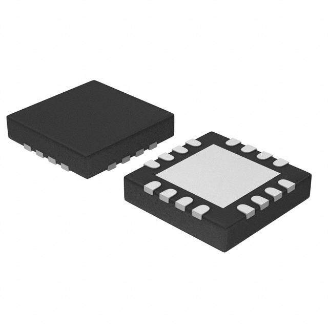
| 产品图片 |
|
| rohs | 符合RoHS无铅 / 符合限制有害物质指令(RoHS)规范要求 |
| 产品系列 | 电源管理 IC,低压差稳压器,Texas Instruments LP3871EMP-5.0/NOPB- |
| 数据手册 | |
| 产品型号 | LP3871EMP-5.0/NOPB |
| PSRR/纹波抑制—典型值 | 57 dB |
| 产品 | Fast Ultra Low Dropout Linear Regulator |
| 产品种类 | 低压差稳压器 |
| 供应商器件封装 | SOT-223-5 |
| 其它名称 | LP3871EMP-5.0/NOPBDKR |
| 包装 | Digi-Reel® |
| 商标 | Texas Instruments |
| 回动电压—最大值 | 350 mV |
| 安装类型 | 表面贴装 |
| 安装风格 | SMD/SMT |
| 封装 | Reel |
| 封装/外壳 | TO-261-5,TO-261AB |
| 封装/箱体 | SOT-223-5 |
| 工作温度 | -40°C ~ 125°C |
| 工厂包装数量 | 1000 |
| 最大工作温度 | + 125 C |
| 最大输入电压 | 7 V |
| 最小工作温度 | - 40 C |
| 最小输入电压 | 2.5 V |
| 标准包装 | 1 |
| 电压-跌落(典型值) | 0.24V @ 800mA |
| 电压-输入 | 最高 7V |
| 电压-输出 | 5V |
| 电流-输出 | 800mA |
| 电流-限制(最小值) | - |
| 稳压器拓扑 | 正,固定式 |
| 稳压器数 | 1 |
| 类型 | Ultra Low Dropout Voltage |
| 系列 | LP3871 |
| 线路调整率 | 0.06 % |
| 设计资源 | http://www.digikey.com/product-highlights/cn/zh/texas-instruments-webench-design-center/3176 |
| 负载调节 | 0.1 % |
| 输出电压 | 5 V |
| 输出电压容差 | +/- 3 % |
| 输出电流 | 800 mA |
| 输出端数量 | 1 Output |
| 输出类型 | Fixed |


- 商务部:美国ITC正式对集成电路等产品启动337调查
- 曝三星4nm工艺存在良率问题 高通将骁龙8 Gen1或转产台积电
- 太阳诱电将投资9.5亿元在常州建新厂生产MLCC 预计2023年完工
- 英特尔发布欧洲新工厂建设计划 深化IDM 2.0 战略
- 台积电先进制程称霸业界 有大客户加持明年业绩稳了
- 达到5530亿美元!SIA预计今年全球半导体销售额将创下新高
- 英特尔拟将自动驾驶子公司Mobileye上市 估值或超500亿美元
- 三星加码芯片和SET,合并消费电子和移动部门,撤换高东真等 CEO
- 三星电子宣布重大人事变动 还合并消费电子和移动部门
- 海关总署:前11个月进口集成电路产品价值2.52万亿元 增长14.8%


PDF Datasheet 数据手册内容提取
Product Sample & Technical Tools & Support & Folder Buy Documents Software Community LP3871,LP3874 SNVS225H–FEBRUARY2003–REVISEDJUNE2015 LP387x 0.8-A Fast Ultra-Low-Dropout Linear Regulators 1 Features 3 Description • InputVoltage:2.5Vto7V The LP3871 and LP3874 series of fast ultra-low- 1 dropout linear regulators operate from a 2.5-V to 7-V • Ultra-Low-DropoutVoltage input supply. Wide range of preset output voltage • LowGroundPinCurrent options are available. These ultra-low-dropout linear • LoadRegulationof0.04% regulators respond very quickly to step changes in load, which makes them suitable for low voltage • 10-nAQuiescentCurrentinShutdownMode microprocessor applications. The devices are • SpecifiedOutputCurrentof0.8-ADC developed on a CMOS process which allows low • OutputVoltageAccuracy ±1.5% quiescent current operation independent of output load current. This CMOS process also allows the • ERROR FlagIndicatesOutputStatus LP3871 and LP3874 to operate under extremely low • SENSEOptionImprovesLoadRegulation dropoutconditions. • MinimumOutputCapacitorRequirements Dropout Voltage: Ultra-low-dropout voltage; typically • Overtemperature/OvercurrentProtection 24 mV at 80-mA load current and 240 mV at 0.8-A • −40°Cto+125°CJunctionTemperatureRange loadcurrent. Ground Pin Current: Typically 6 mA at 0.8-A load 2 Applications current. • MicroprocessorPowerSupplies Shutdown Mode: Typically 10-nA quiescent current • GTL,GTL+,BTL,andSSTLBusTerminators whenthe SDpinispulledlow. • PowerSuppliesforDSPs ERROR Flag: ERROR flag goes low when the output • SCSITerminator voltagedrops10%belownominalvalue. • PostRegulators SENSE: SENSE pin improves regulation at remote • High-EfficiencyLinearRegulators loads. • BatteryChargers Precision Output Voltage: Multiple output voltage • OtherBattery-PoweredApplications options are available ranging from 1.8 V to 5 V with a ensured accuracy of ±1.5% at room temperature, and ±3% over all conditions (varying line, load, and temperature). DeviceInformation(1) PARTNUMBER PACKAGE BODYSIZE(NOM) LP3871 SOT-223(5) 6.50mmx3.56mm LP3874 DDPAK/TO-263(5) 10.16mmx8.42mm (1) For all available packages, see the orderable addendum at theendofthedatasheet. TypicalApplications *SDmustbepulledhighthrougha10-kΩ pullupresistor.SeeApplicationand *SDandERRORpinsmustbepulledhigh Implementationformoreinformation. througha10-kΩpullupresistor.Connect theERRORpintogroundifthisfunctionis notused.SeeApplicationand Implementationformoreinformation. 1 An IMPORTANT NOTICE at the end of this data sheet addresses availability, warranty, changes, use in safety-critical applications, intellectualpropertymattersandotherimportantdisclaimers.PRODUCTIONDATA.
LP3871,LP3874 SNVS225H–FEBRUARY2003–REVISEDJUNE2015 www.ti.com Table of Contents 1 Features.................................................................. 1 7.4 DeviceFunctionalModes..........................................9 2 Applications........................................................... 1 8 ApplicationandImplementation........................ 11 3 Description............................................................. 1 8.1 ApplicationInformation............................................11 4 RevisionHistory..................................................... 2 8.2 TypicalApplications ...............................................11 5 PinConfigurationandFunctions......................... 3 9 PowerSupplyRecommendations...................... 16 9.1 PowerDissipation ..................................................16 6 Specifications......................................................... 4 10 Layout................................................................... 16 6.1 AbsoluteMaximumRatings......................................4 6.2 ESDRatings..............................................................4 10.1 LayoutGuidelines.................................................16 6.3 RecommendedOperatingConditions.......................4 10.2 LayoutExamples...................................................16 6.4 ThermalInformation..................................................4 11 DeviceandDocumentationSupport................. 17 6.5 ElectricalCharacteristics...........................................5 11.1 RelatedLinks........................................................17 6.6 TypicalCharacteristics..............................................7 11.2 CommunityResources..........................................17 7 DetailedDescription.............................................. 8 11.3 Trademarks...........................................................17 7.1 Overview...................................................................8 11.4 ElectrostaticDischargeCaution............................17 7.2 FunctionalBlockDiagrams.......................................8 11.5 Glossary................................................................17 7.3 FeatureDescription...................................................8 12 Mechanical,Packaging,andOrderable Information........................................................... 17 4 Revision History NOTE:Pagenumbersforpreviousrevisionsmaydifferfrompagenumbersinthecurrentversion. ChangesfromRevisionG(April2013)toRevisionH Page • AddedPinConfigurationandFunctionssection,ESDRatingtable,FeatureDescription,DeviceFunctionalModes, ApplicationandImplementation,PowerSupplyRecommendations,Layout,DeviceandDocumentationSupport, andMechanical,Packaging,andOrderableInformationsections;conformpinnamesingraphicstoTInomenclature.......1 • DeletedLeadtemperaturerow-informationinPOA ............................................................................................................ 4 • DeletedHeatsinkingsubsectionsregardingspecificpackagesasspecshavebeenupdated(seeThermal Information).......................................................................................................................................................................... 16 • Changedlayoutexamplestoeliminateobsoletethermal-valuereferences ........................................................................ 16 ChangesfromRevisionF(April2013)toRevisionG Page • ChangedlayoutofNationalDataSheettoTIformat........................................................................................................... 16 2 SubmitDocumentationFeedback Copyright©2003–2015,TexasInstrumentsIncorporated ProductFolderLinks:LP3871 LP3874
LP3871,LP3874 www.ti.com SNVS225H–FEBRUARY2003–REVISEDJUNE2015 5 Pin Configuration and Functions KTTPackage 5-PinDDPAK/TO-263 TopView NCPackage 5-PinSOT-223 TopView GND 5 1 2 3 4 SD IN OUT ERROR /SENSE PinFunctions PIN LP3871 LP3874 TYPE DESCRIPTION NAME SOT-223 DDPAK/TO-263 SOT-223 DDPAK/TO-263 ERROR 4 5 — — O ERRORFlag GND 5 3 5 3 GND Ground IN 2 2 2 2 I Inputvoltage OUT 3 4 3 4 O Outputvoltage SD 1 1 1 1 I Shutdown SENSE — — 4 5 I Remotevoltagesense Copyright©2003–2015,TexasInstrumentsIncorporated SubmitDocumentationFeedback 3 ProductFolderLinks:LP3871 LP3874
LP3871,LP3874 SNVS225H–FEBRUARY2003–REVISEDJUNE2015 www.ti.com 6 Specifications 6.1 Absolute Maximum Ratings overoperatingfree-airtemperaturerange(unlessotherwisenoted)(1)(2) MIN MAX UNIT Inputsupplyvoltage(survival) −0.3 7.5 V Shutdowninputvoltage(survival) −0.3 7.5 V Outputvoltage(survival)(3)(4) −0.3 6 V I (survival) Short-circuitprotected OUT MaximumvoltageforERRORPin V V IN MaximumvoltageforSENSEPin V V OUT Powerdissipation(5) InternallyLimited Storagetemperature,T −65 150 °C stg (1) StressesbeyondthoselistedunderAbsoluteMaximumRatingsmaycausepermanentdamagetothedevice.Thesearestressratings only,whichdonotimplyfunctionaloperationofthedeviceattheseoranyotherconditionsbeyondthoseindicatedunderRecommended OperatingConditions.Exposuretoabsolute-maximum-ratedconditionsforextendedperiodsmayaffectdevicereliability. (2) IfMilitary/Aerospacespecifieddevicesarerequired,pleasecontacttheTISalesOffice/Distributorsforavailabilityandspecifications. (3) Ifusedinadual-supplysystemwheretheregulatorloadisreturnedtoanegativesupply,theoutputmustbediode-clampedtoground. (4) TheoutputPMOSstructurecontainsadiodebetweentheINandOUTpins.Thisdiodeisnormallyreversebiased.Thisdiodewillget forwardbiasedifthevoltageattheoutputterminalisforcedtobehigherthanthevoltageattheinputterminal.Thisdiodecantypically withstand200mAofDCcurrentand1Aofpeakcurrent. (5) Internalthermalshutdowncircuitryprotectsthedevicefrompermanentdamage. 6.2 ESD Ratings VALUE UNIT Human-bodymodel(HBM),perANSI/ESDA/JEDECJS-001(1) ±2000 V Electrostaticdischarge V (ESD) Charged-devicemodel(CDM),perJEDECspecificationJESD22-C101(2) ±500 (1) JEDECdocumentJEP155statesthat500-VHBMallowssafemanufacturingwithastandardESDcontrolprocess. (2) JEDECdocumentJEP157statesthat250-VCDMallowssafemanufacturingwithastandardESDcontrolprocess. 6.3 Recommended Operating Conditions overoperatingfree-airtemperaturerange(unlessotherwisenoted) MIN MAX UNIT Inputsupplyvoltage(1) 2.5 7 V Shutdowninputvoltage −0.3 7 V Maximumoperatingcurrent(DC) 0.8 A Junctiontemperature −40 125 °C (1) TheminimumoperatingvalueforV isequaltoeither[V +V ]or2.5V,whicheverisgreater. IN OUT(NOM) DROPOUT 6.4 Thermal Information LP3871,LP3874 THERMALMETRIC(1) NC(SOT-223) KTT(DDPAK/TO-263) UNIT 5PINS 5PINS R Junction-to-ambientthermalresistance 65.2 40.3 °C/W θJA R Junction-to-case(top)thermalresistance 47.2 43.4 °C/W θJC(top) R Junction-to-boardthermalresistance 9.9 23.1 °C/W θJB ψ Junction-to-topcharacterizationparameter 3.4 11.5 °C/W JT ψ Junction-to-boardcharacterizationparameter 9.7 22 °C/W JB R Junction-to-case(bottom)thermalresistance — 1 °C/W θJC(bot) (1) Formoreinformationabouttraditionalandnewthermalmetrics,seetheSemiconductorandICPackageThermalMetricsapplication report,SPRA953. 4 SubmitDocumentationFeedback Copyright©2003–2015,TexasInstrumentsIncorporated ProductFolderLinks:LP3871 LP3874
LP3871,LP3874 www.ti.com SNVS225H–FEBRUARY2003–REVISEDJUNE2015 6.5 Electrical Characteristics Unlessotherwisespecified:T =25°C,V =V +1V,I =10mA,C =10µF,V =2V. J IN O(NOM) L OUT SD PARAMETER TESTCONDITIONS MIN(1) TYP(2) MAX(1) UNIT Outputvoltagetolerance(3) V +1V≤V ≤7V,10mA≤I ≤0.8A –1.5% 0% 1.5% OUT IN L VOUT VOUT+1V≤VIN≤7V,10mA≤IL≤0.8A, –3% 3% –40°C≤T ≤125°C J Outputvoltagelineregulation(3) V +1V≤V ≤7V 0.02% OUT IN ΔV OL V +1V≤V ≤7V,–40°C≤T ≤125°C 0.06% OUT IN J ΔVO/ Outputvoltageloadregulation(3) 10mA≤IL≤0.8A 0.04% ΔIOUT 10mA≤IL≤0.8A,–40°C≤TJ≤125°C 0.1% I =80mA 24 35 L VIN– Dropoutvoltage(4) IL=80mA,–40°C≤TJ≤125°C 40 mV VOUT IL=0.8A 240 300 I =0.8A,–40°C≤T ≤125°C 350 L J I =150mA 5 9 L Groundpincurrentinnormal IL=150mA,–40°C≤TJ≤125°C 10 I mA GND operationmode I =0.8A 6 14 L I =0.8A,–40°C≤T ≤125°C 15 L J Groundpincurrentinshutdown V ≤0.3V 0.01 10 µA SD IGND mode –40°C≤T ≤85°C 50 J I Peakoutputcurrent V ≥V –4% 1 A O(PK) OUT O(NOM) SHORTCIRCUITPROTECTION I Short-circuitcurrent 2.3 A SC SHUTDOWNINPUT Output=High V IN Output=High,–40°C≤T ≤125°C 2 J V Shutdownthreshold V SDT Output=Low 0 Output=Low,–40°C≤T ≤125°C 0.3 J T Turnoffdelay I =0.8A 20 µs dOFF L T Turnondelay I =0.8A 25 µs dON L I SDinputcurrent V =V 1 nA SD SD IN ERRORFLAG Threshold See(5) 10% V T See(5),–40°C≤T ≤125°C 5% 16% J Thresholdhysteresis See(5) 5% V TH See(5),–40°C≤T ≤125°C 2% 8% J I =100µA 0.02 sink V ERRORflagsaturation V EF(Sat) I =100µA,–40°C≤T ≤125°C 0.1 sink J Td Flagresetdelay 1 µs I ERRORflagpinleakagecurrent 1 nA lk I ERRORflagpinsinkcurrent V =0.5V 1 mA max Error (1) Limitsarespecifiedbytesting,design,orstatisticalcorrelation. (2) Typicalnumbersareat25°Candrepresentthemostlikelyparametricnorm. (3) Outputvoltagelineregulationisdefinedasthechangeinoutputvoltagefromthenominalvalueduetochangeintheinputlinevoltage. Outputvoltageloadregulationisdefinedasthechangeinoutputvoltagefromthenominalvalueduetochangeinloadcurrent.Theline andloadregulationspecificationcontainsonlythetypicalnumber.However,thelimitsforlineandloadregulationareincludedinthe outputvoltagetolerancespecification. (4) Dropoutvoltageisdefinedastheminimuminputtooutputdifferentialvoltageatwhichtheoutputdrops2%belowthenominalvalue. Dropoutvoltagespecificationappliesonlytooutputvoltagesof2.5Vandabove.Foroutputvoltagesbelow2.5V,thedropoutvoltageis nothingbuttheinputtooutputdifferential,becausetheminimuminputvoltageis2.5V. (5) ERRORFlagthresholdandhysteresisarespecifiedaspercentageofregulatedoutputvoltage.SeeERRORFlagOperation. Copyright©2003–2015,TexasInstrumentsIncorporated SubmitDocumentationFeedback 5 ProductFolderLinks:LP3871 LP3874
LP3871,LP3874 SNVS225H–FEBRUARY2003–REVISEDJUNE2015 www.ti.com Electrical Characteristics (continued) Unlessotherwisespecified:T =25°C,V =V +1V,I =10mA,C =10µF,V =2V. J IN O(NOM) L OUT SD PARAMETER TESTCONDITIONS MIN(1) TYP(2) MAX(1) UNIT ACPARAMETERS V =V +1V,C =10µF IN OUT OUT 73 V =3.3V,ƒ=120Hz OUT PSRR Ripplerejection dB V =V +0.5V,C =10µF IN OUT OUT 57 V =3.3V,ƒ=120Hz OUT ρ Outputnoisedensity ƒ=120Hz 0.8 µV n(l/f) BW=10Hz–100kHz,V =2.5V 150 OUT e Outputnoisevoltage µV n RMS BW=300Hz–300kH,V =2.5V 100 OUT 6 SubmitDocumentationFeedback Copyright©2003–2015,TexasInstrumentsIncorporated ProductFolderLinks:LP3871 LP3874
LP3871,LP3874 www.ti.com SNVS225H–FEBRUARY2003–REVISEDJUNE2015 6.6 Typical Characteristics Unlessotherwisespecified:T =25°C,C =10µF,C =10µF,SDpinistiedtoV ,V =2.5V,V =V +1V, J OUT IN IN OUT IN O(NOM) I =10mA. L 500 6 5 400 _ OPOUT VOLTAGE (mV) 230000 21-4520o5CooCC UND PIN CURRENT (mA) 234 DR 100 GRO 1 0 0 1.8 2.3 2.8 3.3 3.8 4.3 5.0 0 0.5 1.0 LOAD CURRENT (A) OUTPUT VOLTAGE (V) I =800mA L Figure1.DropoutVoltagevsOutputLoadCurrent Figure2.GroundCurrentvsOutputVoltage 10 14 1 V)OUT 12 A)P % of 10 WN I (Q 0.1 HOLD ( 8 O S 6 D E T R U H H T 4 S 0.01 R O R 2 R E 0.001 0 -40 -20 0 20 40 60 80 100 125 -40 -20 0 20 40 60 80 100 125 TEMPERATURE (oC) JUNCTION TEMPERATURE (oC) Figure3.ShutdownI vsJunctionTemperature Figure4.ERRORFlagThresholdvsJunctionTemperature Q 3 3 2.5 mV) 2.5 AD REGULATION (mV/A) 1.512 OLT CHANGE in V (IN 1.512 O V DC L 0.5 V/OUT 0.5 ' 0 0 -40 -20 0 20 40 60 80 100 125 -40 -20 0 20 40 60 80 100 125 JUNCTION TEMPERATURE (oC) JUNCTION TEMPERATURE (oC) Figure5.DCLoadRegulationvsJunctionTemperature Figure6.DCLineRegulationvsTemperature Copyright©2003–2015,TexasInstrumentsIncorporated SubmitDocumentationFeedback 7 ProductFolderLinks:LP3871 LP3874
LP3871,LP3874 SNVS225H–FEBRUARY2003–REVISEDJUNE2015 www.ti.com 7 Detailed Description 7.1 Overview The LP3871 and LP3874 linear regulators are designed to provide an ultra-low-dropout voltage with excellent transient response and load/line regulation. For battery-powered always-on type applications, the very low quiescent current of LP3871 and LP3874 in shutdown mode helps reduce battery drain. For applications where load is not placed close to the regulator, LP3874 incorporates a voltage sense circuit to improve voltage regulation at the point of load. The ERROR output pin of LP3871 can be used in the system to flag a low-voltage condition. 7.2 Functional Block Diagrams Figure7. LP3871BlockDiagram Figure8. LP3874BlockDiagram 7.3 Feature Description 7.3.1 Shutdown(SD) The LM3871 and LP3874 devices have a shutdown feature that turns the device off and reduces the quiescent currentto10nA,typical. 8 SubmitDocumentationFeedback Copyright©2003–2015,TexasInstrumentsIncorporated ProductFolderLinks:LP3871 LP3874
LP3871,LP3874 www.ti.com SNVS225H–FEBRUARY2003–REVISEDJUNE2015 Feature Description (continued) 7.3.2 Short-CircuitProtection The LP3871and LP3874 devices are short-circuit protected and, in the event of a peak overcurrent condition, the short-circuitcontrolloopwillrapidlydrivetheoutputPMOSpasselementoff.Oncethepowerpasselementshuts down, the control loop will rapidly cycle the output on and off until the average power dissipation causes the thermalshutdowncircuittorespondtoservotheon/offcyclingtoalowerfrequency. 7.3.3 LowDropoutVoltage TheLP3871andLP3874devicesfeatureanultra-low-dropoutvoltage,typically24mVat80-mAloadcurrentand 240mVat0.8-Aloadcurrent. The dropout voltage of a regulator is defined as the minimum input-to-output differential required to stay within 2% of the nominal output voltage. For CMOS LDOs, the dropout voltage is the product of the load current and theR oftheinternalMOSFET. ds(on) 7.3.4 SENSEPin In applications where the regulator output is not very close to the load, LP3874 can provide better remote load regulation using the SENSE pin. Figure 9 depicts the advantage of the SENSE option. LP3871 regulates the voltage at the OUT pin. Hence, the voltage at the remote load will be the regulator output voltage minus the drop across the trace resistance. For example, in the case of a 3.3-V output, if the trace resistance is 100 mΩ, the voltage at the remote load will be 3.22 V with 0.8 A of load current, I . The LP3874 regulates the voltage at LOAD the SENSE pin. Connecting the SENSE pin to the remote load will provide regulation at the remote load, as showninFigure9.IftheSENSEoptionpinisnotrequired,theSENSEpinmustbeconnectedtotheOUTpin. Figure9. ImprovingRemoteLoadRegulationusingLP3874 7.4 Device Functional Modes 7.4.1 ShutdownMode A CMOS logic low level signal at the shutdown (SD) pin will turn off the regulator. The SD pin must be actively terminated through a 10-kΩ pullup resistor for a proper operation. If this pin is driven from a source that actively pulls high and low (such as a CMOS rail-to-rail comparator), the pullup resistor is not required. This pin must be tiedtoV ifnotused. IN 7.4.2 ActiveMode When voltage at SD pin of the LP3871 and LP3874 devices is at logic high level, the device is in normal mode of operation. Copyright©2003–2015,TexasInstrumentsIncorporated SubmitDocumentationFeedback 9 ProductFolderLinks:LP3871 LP3874
LP3871,LP3874 SNVS225H–FEBRUARY2003–REVISEDJUNE2015 www.ti.com Device Functional Modes (continued) 7.4.3 ERROR FlagOperation The LP3871 produces logic low signals at the ERROR Flag pin when the output drops out of regulation due to low input voltage, current limiting, or thermal limiting. This flag has a built-in hysteresis. The timing diagram in Figure 10 shows the relationship between the ERROR flag and the output voltage. In this example, the input voltageischangedtodemonstratethefunctionalityofthe ERROR Flag. The internal ERROR flag comparator has an open drain output stage. Hence, the ERROR pin must be pulled high through a pullup resistor. Although the ERROR flag pin can sink current of 1mA, this current is energy drain from the input supply. Hence, the value of the pullup resistor must be in the range of 10 kΩ to 1 MΩ. The ERROR pin must be connected to ground if this function is not used. It must also be noted that when the shutdown pin is pulled low, the ERROR pin is forced to be invalid for reasons of saving power in shutdown mode. Figure10. ERROR FlagOperation 10 SubmitDocumentationFeedback Copyright©2003–2015,TexasInstrumentsIncorporated ProductFolderLinks:LP3871 LP3874
LP3871,LP3874 www.ti.com SNVS225H–FEBRUARY2003–REVISEDJUNE2015 8 Application and Implementation NOTE Information in the following applications sections is not part of the TI component specification, and TI does not warrant its accuracy or completeness. TI’s customers are responsible for determining suitability of components for their purposes. Customers must validateandtesttheirdesignimplementationtoconfirmsystemfunctionality. 8.1 Application Information The LP3871 and LP3874 devices are linear regulators designed to provide high load current of up to 0.8 A, low dropoutvoltage,andlowquiescentcurrentinshutdownmode. 8.1.1 ReverseCurrentPath The internal MOSFET in LP3871 and LP3874 has an inherent parasitic diode. During normal operation, the input voltage is higher than the output voltage and the parasitic diode is reverse biased. However, if the output is pulledabovetheinputinanapplication,thencurrentflowsfromtheoutputtotheinputastheparasiticdiodegets forwardbiased.Theoutputcanbepulledabovetheinputaslongasthecurrentintheparasiticdiodeislimitedto 200-mAcontinuousand1-Apeak. 8.1.2 TurnonCharacteristicsforOutputVoltagesProgrammedTo2VorBelow As V increases during start-up, the regulator output will track the input until V reaches the minimum operating IN IN voltage (typically about 2.5 V). For output voltages programmed to 2 V or below, the regulator output may momentarily exceed its programmed output voltage during start-up. Outputs programmed to voltages above 2 V arenotaffectedbythisbehavior. 8.2 Typical Applications *SDandERRORpinsmustbepulledhighthrougha10-kΩpullupresistor.ConnecttheERRORpintogroundifthis functionisnotused. Figure11. LP3871TypicalApplication *SDmustbepulledhighthrougha10-kΩpullupresistor. Figure12. LP3874TypicalApplication Copyright©2003–2015,TexasInstrumentsIncorporated SubmitDocumentationFeedback 11 ProductFolderLinks:LP3871 LP3874
LP3871,LP3874 SNVS225H–FEBRUARY2003–REVISEDJUNE2015 www.ti.com Typical Applications (continued) 8.2.1 DesignRequirements ForLP3871andLP3874typicalapplications,usetheparameterslistedinTable1. Table1.DesignParameters DESIGNPARAMETER EXAMPLEVALUE Inputvoltage 2.5Vto7V Outputvoltage 2.5V Outputcurrent 0.8A Outputcapacitor 10µF Inputcapacitor 10µF OutputcapacitorESRrange 100mΩto4Ω 8.2.2 DetailedDesignProcedure 8.2.2.1 ExternalCapacitors Like any low-dropout regulator, external capacitors are required to assure stability. These capacitors must be correctlyselectedforproperperformance. • Input Capacitor: An input capacitor of at least 10 μF is required. Ceramic, tantalum, or Electrolytic capacitors maybeused,andcapacitancemaybeincreasedwithoutlimit. • Output Capacitor: An output capacitor is required for loop stability. It must be located less than 1 cm from the device and connected directly to the output and ground pins using traces which have no other currents flowingthroughthem(seeLayoutGuidelines). The minimum value of output capacitance that can be used for stable full-load operation is 10 µF, but it may be increased without limit. The output capacitor must have an equivalent series resistance (ESR) value as shown in thestableregionofthecurve(Figure13).Tantalumcapacitorsarerecommendedfortheoutputcapacitor. 10 1.0 COUT > 10PF ): STABLE REGION R ( S 0.1 E OUT C .01 .001 0 0.2 0.4 0.6 0.8 1 LOAD CURRENT (A) Figure13. ESRCurve 8.2.2.2 SelectingaCapacitor It is important to note that capacitance tolerance and variation with temperature must be taken into consideration when selecting a capacitor so that the minimum required amount of capacitance is provided over the full operating temperature range. In general, a good Tantalum capacitor will show very little capacitance variation with temperature, but a ceramic may not be as good (depending on dielectric type). Aluminum electrolytics also typicallyhavelargetemperaturevariationofcapacitancevalue. Equally important to consider is a capacitor's ESR change with temperature: this is not an issue with ceramics, as their ESR is extremely low. However, it is very important in Tantalum and aluminum electrolytic capacitors. Both show increasing ESR at colder temperatures, but the increase in aluminum electrolytic capacitors is so severetheymaynotbefeasibleforsomeapplications(seeCapacitorCharacteristics). 12 SubmitDocumentationFeedback Copyright©2003–2015,TexasInstrumentsIncorporated ProductFolderLinks:LP3871 LP3874
LP3871,LP3874 www.ti.com SNVS225H–FEBRUARY2003–REVISEDJUNE2015 8.2.2.3 CapacitorCharacteristics 8.2.2.3.1 Ceramic For values of capacitance in the 10-µF to 100-µF range, ceramics are usually larger and more costly than tantalum capacitors but give superior AC performance for bypassing high frequency noise because of very low ESR (typically less than 10 mΩ). However, some dielectric types do not have good capacitance characteristics asafunctionofvoltageandtemperature. Z5U and Y5V dielectric ceramics have capacitance that drops severely with applied voltage. A typical Z5U or Y5Vcapacitorcanlose60%ofitsratedcapacitancewithhalfoftheratedvoltageappliedtoit.TheZ5UandY5V also exhibit a severe temperature effect, losing more than 50% of nominal capacitance at high and low limits of thetemperaturerange. X7R and X5R dielectric ceramic capacitors are strongly recommended if ceramics are used, as they typically maintain a capacitance range within ±20% of nominal over full operating ratings of temperature and voltage. Of course,theyaretypicallylargerandmorecostlythanZ5U/Y5Utypesforagivenvoltageandcapacitance. 8.2.2.3.2 Tantalum Solid tantalum capacitors are recommended for use on the output because their typical ESR is very close to the ideal value required for loop compensation. They also work well as input capacitors if selected to meet the ESR requirementspreviouslylisted. Tantalums also have good temperature stability: a good quality tantalum will typically show a capacitance value that varies less than 10-15% across the full temperature range of 125°C to −40°C. ESR will vary only about 2X goingfromthehightolowtemperaturelimits. The increasing ESR at lower temperatures can cause oscillations when marginal quality capacitors are used (if theESRofthecapacitorisneartheupperlimitofthestabilityrangeatroomtemperature). 8.2.2.3.3 Aluminum This capacitor type offers the most capacitance for the money. The disadvantages are that they are larger in physical size, not widely available in surface mount, and have poor AC performance (especially at higher frequencies)duetohigherESRandESL. Compared by size, the ESR of an aluminum electrolytic is higher than either tantalum or ceramic, and it also varies greatly with temperature. A typical aluminum electrolytic can exhibit an ESR increase of as much as 50× whengoingfrom25°Cdownto −40°C. It must also be noted that many aluminum electrolytics only specify impedance at a frequency of 120 Hz, which indicates they have poor high frequency performance. Only aluminum electrolytics that have an impedance specified at a higher frequency (between 20 kHz and 100 kHz) must be used for the LP387X. Derating must be appliedtothemanufacturer'sESRspecification,sinceitistypicallyonlyvalidatroomtemperature. Any applications using aluminum electrolytics must be thoroughly tested at the lowest ambient operating temperaturewhereESRismaximum. 8.2.2.4 RFI/EMISusceptibility Radio frequency interference (RFI) and electromagnetic interference (EMI) can degrade the performance of any integrated circuit because of the small dimensions of the geometries inside the device. In applications where circuit sources are present which generate signals with significant high frequency energy content (> 1 MHz), care mustbetakentoensurethatthisdoesnotaffectthedeviceregulator. If RFI/EMI noise is present on the input side of the regulator (such as applications where the input source comes from the output of a switching regulator), good ceramic bypass capacitors must be used at the input pin of the device. If a load is connected to the device output which switches at high speed (such as a clock), the high-frequency currentpulsesrequiredbytheloadmustbesuppliedbythecapacitorsonthedeviceoutput.Sincethebandwidth of the regulator loop is less than 100 kHz, the control circuitry cannot respond to load changes above that frequency. This means the effective output impedance of the device at frequencies above 100 kHz is determined onlybytheoutputcapacitor(s). Copyright©2003–2015,TexasInstrumentsIncorporated SubmitDocumentationFeedback 13 ProductFolderLinks:LP3871 LP3874
LP3871,LP3874 SNVS225H–FEBRUARY2003–REVISEDJUNE2015 www.ti.com In applications where the load is switching at high speed, the output of the device may need RF isolation from the load. It is recommended that some inductance be placed between the output capacitor and the load, and goodRFbypasscapacitorsbeplaceddirectlyacrosstheload. PCB layout is also critical in high noise environments, since RFI/EMI is easily radiated directly into PC traces. Noisy circuitry must be isolated from "clean" circuits where possible, and grounded through a separate path. At MHz frequencies, ground planes begin to look inductive and RFI/EMI can cause ground bounce across the groundplane. In multi-layer PCB applications, care must be taken in layout so that noisy power and ground planes do not radiatedirectlyintoadjacentlayerswhichcarryanalogpowerandground. 8.2.2.5 OutputNoise Noiseisspecifiedintwoways: • SpotNoise(orOutputNoiseDensity):theRMSsumofallnoisesources,measuredattheregulatoroutput,at a specific frequency (measured with a 1-Hz bandwidth). This type of noise is usually plotted on a curve as a functionoffrequency. • Total Output Noise (or Broad-Band Noise): the RMS sum of spot noise over a specified bandwidth, usually severaldecadesoffrequencies. Attention must be paid to the units of measurement. Spot noise is measured in units µV/√Hz or nV/√Hz and total outputnoiseismeasuredinµV . RMS The primary source of noise in low-dropout regulators is the internal reference. In CMOS regulators, noise has a low frequency component and a high frequency component, which depend strongly on the silicon area and quiescent current. Noise can be reduced in two ways: by increasing the transistor area or by increasing the current drawn by the internal reference. Increasing the area will decrease the chance of fitting the die into a smaller package. Increasing the current drawn by the internal reference increases the total supply current (ground pin current). Using an optimized trade-off of ground pin current and die size, the LP3871 and LP3874 achievelownoiseperformanceandlowquiescent-currentoperation. The total output noise specification for LP3871 and LP3874 devices is presented in Electrical Characteristics. TheoutputnoisedensityatdifferentfrequenciesisrepresentedbyacurveunderTypicalCharacteristics. 14 SubmitDocumentationFeedback Copyright©2003–2015,TexasInstrumentsIncorporated ProductFolderLinks:LP3871 LP3874
LP3871,LP3874 www.ti.com SNVS225H–FEBRUARY2003–REVISEDJUNE2015 8.2.3 ApplicationCurves Unlessotherwisespecified:T =25°C,C =10µF,C =10µF,SDpinistiedtoV ,V =2.5V,V =V +1V, J OUT IN IN OUT IN O(NOM) I =10mA. L 100VmOVU/TDIV VOUT 100mV/DIV MAGNITUDE MAGNITUDE 1AILO/DADIV 1AILO/DADIV TIME (50Ps/DIV) TIME (50Ps/DIV) CIN=COUT=10µF,Oscon CIN=COUT=100µF,Oscon Figure14.LoadTransientResponse Figure15.LoadTransientResponse 100VmOVU/TDIV 100VmOVU/TDIV MAGNITUDE MAGNITUDE ILOAD ILOAD 1A/DIV 1A/DIV TIME (50Ps/DIV) TIME (50Ps/DIV) C =C =10µF,Poscap C =C =10µF,Tantalum IN OUT IN OUT Figure16.LoadTransientResponse Figure17.LoadTransientResponse VOUT 100mV/DIV DE U NIT G A M ILOAD 1A/DIV TIME (50Ps/DIV) C =C =100µF,Tantalum IN OUT Figure18.LoadTransientResponse Copyright©2003–2015,TexasInstrumentsIncorporated SubmitDocumentationFeedback 15 ProductFolderLinks:LP3871 LP3874
LP3871,LP3874 SNVS225H–FEBRUARY2003–REVISEDJUNE2015 www.ti.com 9 Power Supply Recommendations 9.1 Power Dissipation LP3871 and LP3874 can deliver a continuous current of 0.8 A over the full operating temperature range. A heatsink may be required depending on the maximum power dissipation and maximum ambient temperature of the application. Under all possible conditions, the junction temperature must be within the range specified under operatingconditions.Thetotalpowerdissipationofthedeviceisgivenby: 2&=:8+0 F8176;+176+:8+0;+)0& where • I istheoperatinggroundcurrentofthedevice(specifiedunderElectricalCharacteristics). (1) GND The maximum allowable temperature rise (T ) depends on the maximum ambient temperature (T ) of the Rmax Amax application,andthemaximumallowablejunctiontemperature(T ): Jmax 6 =6 F6 4I=T ,I=T #I=T (2) The maximum allowable value for junction to ambient thermal resistance, R , can be calculated using the θJA formula: 4 =6 F6 /2 à,# 4I=T #I=T & (3) 10 Layout 10.1 Layout Guidelines GoodPClayoutpracticesmustbeusedorinstabilitycanbeinducedbecauseofgroundloopsandvoltagedrops. The input and output capacitors must be directly connected to the input, output, and ground pins of the regulator usingtraceswhichdonothaveothercurrentsflowinginthem(Kelvinconnect). The best way to do this is to lay out C and C near the device with short traces to the IN, OUT, and ground IN OUT pins. The regulator ground pin must be connected to the external circuit ground so that the regulator and its capacitorshavea"singlepointground". It must be noted that stability problems have been seen in applications where "vias" to an internal ground plane were used at the ground points of the device and the input and output capacitors. This was caused by varying ground potentials at these nodes resulting from current flowing through the ground plane. Using a single point groundtechniquefortheregulatoranditscapacitorsfixedtheproblem. Since high current flows through the traces going into IN and coming from OUT, Kelvin connect the capacitor leadstothesepinssothereisnovoltagedropinserieswiththeinputandoutputcapacitors. 10.2 Layout Examples CIN VIN SD SD IN VIN IN CIN GND GND VOUT OUT COUT OUT ERROR/SENSE COUT VOUT ERROR/SENSE Figure19.LayoutExampleforSOT-223Package Figure20.LayoutExampleforTO-263Package 16 SubmitDocumentationFeedback Copyright©2003–2015,TexasInstrumentsIncorporated ProductFolderLinks:LP3871 LP3874
LP3871,LP3874 www.ti.com SNVS225H–FEBRUARY2003–REVISEDJUNE2015 11 Device and Documentation Support 11.1 Related Links Table 2 lists quick access links. Categories include technical documents, support and community resources, toolsandsoftware,andquickaccesstosampleorbuy. Table2.RelatedLinks TECHNICAL TOOLS& SUPPORT& PARTS PRODUCTFOLDER SAMPLE&BUY DOCUMENTS SOFTWARE COMMUNITY LP3871 Clickhere Clickhere Clickhere Clickhere Clickhere LP3874 Clickhere Clickhere Clickhere Clickhere Clickhere 11.2 Community Resources The following links connect to TI community resources. Linked contents are provided "AS IS" by the respective contributors. They do not constitute TI specifications and do not necessarily reflect TI's views; see TI's Terms of Use. TIE2E™OnlineCommunity TI'sEngineer-to-Engineer(E2E)Community.Createdtofostercollaboration amongengineers.Ate2e.ti.com,youcanaskquestions,shareknowledge,exploreideasandhelp solveproblemswithfellowengineers. DesignSupport TI'sDesignSupport QuicklyfindhelpfulE2Eforumsalongwithdesignsupporttoolsand contactinformationfortechnicalsupport. 11.3 Trademarks E2EisatrademarkofTexasInstruments. Allothertrademarksarethepropertyoftheirrespectiveowners. 11.4 Electrostatic Discharge Caution Thesedeviceshavelimitedbuilt-inESDprotection.Theleadsshouldbeshortedtogetherorthedeviceplacedinconductivefoam duringstorageorhandlingtopreventelectrostaticdamagetotheMOSgates. 11.5 Glossary SLYZ022—TIGlossary. Thisglossarylistsandexplainsterms,acronyms,anddefinitions. 12 Mechanical, Packaging, and Orderable Information The following pages include mechanical, packaging, and orderable information. This information is the most current data available for the designated devices. This data is subject to change without notice and revision of thisdocument.Forbrowser-basedversionsofthisdatasheet,refertotheleft-handnavigation. Copyright©2003–2015,TexasInstrumentsIncorporated SubmitDocumentationFeedback 17 ProductFolderLinks:LP3871 LP3874
PACKAGE OPTION ADDENDUM www.ti.com 9-Jun-2020 PACKAGING INFORMATION Orderable Device Status Package Type Package Pins Package Eco Plan Lead/Ball Finish MSL Peak Temp Op Temp (°C) Device Marking Samples (1) Drawing Qty (2) (6) (3) (4/5) LP3871EMP-1.8/NOPB ACTIVE SOT-223 NDC 5 1000 Green (RoHS SN Level-1-260C-UNLIM -40 to 125 LH6B & no Sb/Br) LP3871EMP-2.5/NOPB ACTIVE SOT-223 NDC 5 1000 Green (RoHS SN Level-1-260C-UNLIM -40 to 125 LH7B & no Sb/Br) LP3871EMP-3.3/NOPB ACTIVE SOT-223 NDC 5 1000 Green (RoHS SN Level-1-260C-UNLIM -40 to 125 LH8B & no Sb/Br) LP3871EMP-5.0/NOPB ACTIVE SOT-223 NDC 5 1000 Green (RoHS SN Level-1-260C-UNLIM -40 to 125 LH9B & no Sb/Br) LP3871EMPX-3.3/NOPB ACTIVE SOT-223 NDC 5 2000 Green (RoHS SN Level-1-260C-UNLIM -40 to 125 LH8B & no Sb/Br) LP3871ES-1.8/NOPB ACTIVE DDPAK/ KTT 5 45 Green (RoHS SN Level-3-245C-168 HR -40 to 125 LP3871ES TO-263 & no Sb/Br) -1.8 LP3871ES-2.5/NOPB ACTIVE DDPAK/ KTT 5 45 Green (RoHS SN Level-3-245C-168 HR -40 to 125 LP3871ES TO-263 & no Sb/Br) -2.5 LP3871ES-3.3/NOPB ACTIVE DDPAK/ KTT 5 45 Green (RoHS SN Level-3-245C-168 HR -40 to 125 LP3871ES TO-263 & no Sb/Br) -3.3 LP3871ESX-1.8/NOPB ACTIVE DDPAK/ KTT 5 500 Green (RoHS SN Level-3-245C-168 HR -40 to 125 LP3871ES TO-263 & no Sb/Br) -1.8 LP3871ESX-2.5/NOPB ACTIVE DDPAK/ KTT 5 500 Green (RoHS SN Level-3-245C-168 HR -40 to 125 LP3871ES TO-263 & no Sb/Br) -2.5 LP3871ESX-3.3/NOPB ACTIVE DDPAK/ KTT 5 500 Green (RoHS SN Level-3-245C-168 HR -40 to 125 LP3871ES TO-263 & no Sb/Br) -3.3 LP3874EMP-1.8/NOPB ACTIVE SOT-223 NDC 5 1000 Green (RoHS SN Level-1-260C-UNLIM -40 to 125 LHEB & no Sb/Br) LP3874EMP-2.5/NOPB ACTIVE SOT-223 NDC 5 1000 Green (RoHS SN Level-1-260C-UNLIM -40 to 125 LHFB & no Sb/Br) LP3874EMP-3.3 NRND SOT-223 NDC 5 1000 TBD Call TI Call TI -40 to 125 LHHB LP3874EMP-3.3/NOPB ACTIVE SOT-223 NDC 5 1000 Green (RoHS SN Level-1-260C-UNLIM -40 to 125 LHHB & no Sb/Br) LP3874EMP-5.0/NOPB ACTIVE SOT-223 NDC 5 1000 Green (RoHS SN Level-1-260C-UNLIM -40 to 125 LHJB & no Sb/Br) LP3874EMPX-1.8/NOPB ACTIVE SOT-223 NDC 5 2000 Green (RoHS SN Level-1-260C-UNLIM -40 to 125 LHEB & no Sb/Br) Addendum-Page 1
PACKAGE OPTION ADDENDUM www.ti.com 9-Jun-2020 Orderable Device Status Package Type Package Pins Package Eco Plan Lead/Ball Finish MSL Peak Temp Op Temp (°C) Device Marking Samples (1) Drawing Qty (2) (6) (3) (4/5) LP3874EMPX-3.3/NOPB ACTIVE SOT-223 NDC 5 2000 Green (RoHS SN Level-1-260C-UNLIM -40 to 125 LHHB & no Sb/Br) LP3874EMPX-5.0/NOPB ACTIVE SOT-223 NDC 5 2000 Green (RoHS SN Level-1-260C-UNLIM -40 to 125 LHJB & no Sb/Br) LP3874ES-2.5/NOPB ACTIVE DDPAK/ KTT 5 45 Green (RoHS SN Level-3-245C-168 HR -40 to 125 LP3874ES TO-263 & no Sb/Br) -2.5 LP3874ES-3.3/NOPB ACTIVE DDPAK/ KTT 5 45 Green (RoHS SN Level-3-245C-168 HR -40 to 125 LP3874ES TO-263 & no Sb/Br) -3.3 (1) The marketing status values are defined as follows: ACTIVE: Product device recommended for new designs. LIFEBUY: TI has announced that the device will be discontinued, and a lifetime-buy period is in effect. NRND: Not recommended for new designs. Device is in production to support existing customers, but TI does not recommend using this part in a new design. PREVIEW: Device has been announced but is not in production. Samples may or may not be available. OBSOLETE: TI has discontinued the production of the device. (2) RoHS: TI defines "RoHS" to mean semiconductor products that are compliant with the current EU RoHS requirements for all 10 RoHS substances, including the requirement that RoHS substance do not exceed 0.1% by weight in homogeneous materials. Where designed to be soldered at high temperatures, "RoHS" products are suitable for use in specified lead-free processes. TI may reference these types of products as "Pb-Free". RoHS Exempt: TI defines "RoHS Exempt" to mean products that contain lead but are compliant with EU RoHS pursuant to a specific EU RoHS exemption. Green: TI defines "Green" to mean the content of Chlorine (Cl) and Bromine (Br) based flame retardants meet JS709B low halogen requirements of <=1000ppm threshold. Antimony trioxide based flame retardants must also meet the <=1000ppm threshold requirement. (3) MSL, Peak Temp. - The Moisture Sensitivity Level rating according to the JEDEC industry standard classifications, and peak solder temperature. (4) There may be additional marking, which relates to the logo, the lot trace code information, or the environmental category on the device. (5) Multiple Device Markings will be inside parentheses. Only one Device Marking contained in parentheses and separated by a "~" will appear on a device. If a line is indented then it is a continuation of the previous line and the two combined represent the entire Device Marking for that device. (6) Lead/Ball Finish - Orderable Devices may have multiple material finish options. Finish options are separated by a vertical ruled line. Lead/Ball Finish values may wrap to two lines if the finish value exceeds the maximum column width. Important Information and Disclaimer:The information provided on this page represents TI's knowledge and belief as of the date that it is provided. TI bases its knowledge and belief on information provided by third parties, and makes no representation or warranty as to the accuracy of such information. Efforts are underway to better integrate information from third parties. TI has taken and continues to take reasonable steps to provide representative and accurate information but may not have conducted destructive testing or chemical analysis on incoming materials and chemicals. TI and TI suppliers consider certain information to be proprietary, and thus CAS numbers and other limited information may not be available for release. Addendum-Page 2
PACKAGE OPTION ADDENDUM www.ti.com 9-Jun-2020 In no event shall TI's liability arising out of such information exceed the total purchase price of the TI part(s) at issue in this document sold by TI to Customer on an annual basis. Addendum-Page 3
PACKAGE MATERIALS INFORMATION www.ti.com 29-Sep-2019 TAPE AND REEL INFORMATION *Alldimensionsarenominal Device Package Package Pins SPQ Reel Reel A0 B0 K0 P1 W Pin1 Type Drawing Diameter Width (mm) (mm) (mm) (mm) (mm) Quadrant (mm) W1(mm) LP3871EMP-1.8/NOPB SOT-223 NDC 5 1000 330.0 16.4 7.0 7.5 2.2 12.0 16.0 Q3 LP3871EMP-2.5/NOPB SOT-223 NDC 5 1000 330.0 16.4 7.0 7.5 2.2 12.0 16.0 Q3 LP3871EMP-3.3/NOPB SOT-223 NDC 5 1000 330.0 16.4 7.0 7.5 2.2 12.0 16.0 Q3 LP3871EMP-5.0/NOPB SOT-223 NDC 5 1000 330.0 16.4 7.0 7.5 2.2 12.0 16.0 Q3 LP3871EMPX-3.3/NOPB SOT-223 NDC 5 2000 330.0 16.4 7.0 7.5 2.2 12.0 16.0 Q3 LP3871ESX-1.8/NOPB DDPAK/ KTT 5 500 330.0 24.4 10.75 14.85 5.0 16.0 24.0 Q2 TO-263 LP3871ESX-2.5/NOPB DDPAK/ KTT 5 500 330.0 24.4 10.75 14.85 5.0 16.0 24.0 Q2 TO-263 LP3871ESX-3.3/NOPB DDPAK/ KTT 5 500 330.0 24.4 10.75 14.85 5.0 16.0 24.0 Q2 TO-263 LP3874EMP-1.8/NOPB SOT-223 NDC 5 1000 330.0 16.4 7.0 7.5 2.2 12.0 16.0 Q3 LP3874EMP-2.5/NOPB SOT-223 NDC 5 1000 330.0 16.4 7.0 7.5 2.2 12.0 16.0 Q3 LP3874EMP-3.3 SOT-223 NDC 5 1000 330.0 16.4 7.0 7.5 2.2 12.0 16.0 Q3 LP3874EMP-3.3/NOPB SOT-223 NDC 5 1000 330.0 16.4 7.0 7.5 2.2 12.0 16.0 Q3 LP3874EMP-5.0/NOPB SOT-223 NDC 5 1000 330.0 16.4 7.0 7.5 2.2 12.0 16.0 Q3 LP3874EMPX-1.8/NOPB SOT-223 NDC 5 2000 330.0 16.4 7.0 7.5 2.2 12.0 16.0 Q3 LP3874EMPX-3.3/NOPB SOT-223 NDC 5 2000 330.0 16.4 7.0 7.5 2.2 12.0 16.0 Q3 LP3874EMPX-5.0/NOPB SOT-223 NDC 5 2000 330.0 16.4 7.0 7.5 2.2 12.0 16.0 Q3 PackMaterials-Page1
PACKAGE MATERIALS INFORMATION www.ti.com 29-Sep-2019 *Alldimensionsarenominal Device PackageType PackageDrawing Pins SPQ Length(mm) Width(mm) Height(mm) LP3871EMP-1.8/NOPB SOT-223 NDC 5 1000 367.0 367.0 35.0 LP3871EMP-2.5/NOPB SOT-223 NDC 5 1000 367.0 367.0 35.0 LP3871EMP-3.3/NOPB SOT-223 NDC 5 1000 367.0 367.0 35.0 LP3871EMP-5.0/NOPB SOT-223 NDC 5 1000 367.0 367.0 35.0 LP3871EMPX-3.3/NOPB SOT-223 NDC 5 2000 367.0 367.0 35.0 LP3871ESX-1.8/NOPB DDPAK/TO-263 KTT 5 500 367.0 367.0 45.0 LP3871ESX-2.5/NOPB DDPAK/TO-263 KTT 5 500 367.0 367.0 45.0 LP3871ESX-3.3/NOPB DDPAK/TO-263 KTT 5 500 367.0 367.0 45.0 LP3874EMP-1.8/NOPB SOT-223 NDC 5 1000 367.0 367.0 35.0 LP3874EMP-2.5/NOPB SOT-223 NDC 5 1000 367.0 367.0 35.0 LP3874EMP-3.3 SOT-223 NDC 5 1000 367.0 367.0 35.0 LP3874EMP-3.3/NOPB SOT-223 NDC 5 1000 367.0 367.0 35.0 LP3874EMP-5.0/NOPB SOT-223 NDC 5 1000 367.0 367.0 35.0 LP3874EMPX-1.8/NOPB SOT-223 NDC 5 2000 367.0 367.0 35.0 LP3874EMPX-3.3/NOPB SOT-223 NDC 5 2000 367.0 367.0 35.0 LP3874EMPX-5.0/NOPB SOT-223 NDC 5 2000 367.0 367.0 35.0 PackMaterials-Page2
MECHANICAL DATA NDC0005A www.ti.com
MECHANICAL DATA KTT0005B TS5B (Rev D) BOTTOM SIDE OF PACKAGE www.ti.com
IMPORTANTNOTICEANDDISCLAIMER TI PROVIDES TECHNICAL AND RELIABILITY DATA (INCLUDING DATASHEETS), DESIGN RESOURCES (INCLUDING REFERENCE DESIGNS), APPLICATION OR OTHER DESIGN ADVICE, WEB TOOLS, SAFETY INFORMATION, AND OTHER RESOURCES “AS IS” AND WITH ALL FAULTS, AND DISCLAIMS ALL WARRANTIES, EXPRESS AND IMPLIED, INCLUDING WITHOUT LIMITATION ANY IMPLIED WARRANTIES OF MERCHANTABILITY, FITNESS FOR A PARTICULAR PURPOSE OR NON-INFRINGEMENT OF THIRD PARTY INTELLECTUAL PROPERTY RIGHTS. These resources are intended for skilled developers designing with TI products. You are solely responsible for (1) selecting the appropriate TI products for your application, (2) designing, validating and testing your application, and (3) ensuring your application meets applicable standards, and any other safety, security, or other requirements. These resources are subject to change without notice. TI grants you permission to use these resources only for development of an application that uses the TI products described in the resource. Other reproduction and display of these resources is prohibited. No license is granted to any other TI intellectual property right or to any third party intellectual property right. TI disclaims responsibility for, and you will fully indemnify TI and its representatives against, any claims, damages, costs, losses, and liabilities arising out of your use of these resources. TI’s products are provided subject to TI’s Terms of Sale (www.ti.com/legal/termsofsale.html) or other applicable terms available either on ti.com or provided in conjunction with such TI products. TI’s provision of these resources does not expand or otherwise alter TI’s applicable warranties or warranty disclaimers for TI products. Mailing Address: Texas Instruments, Post Office Box 655303, Dallas, Texas 75265 Copyright © 2020, Texas Instruments Incorporated