ICGOO在线商城 > 集成电路(IC) > PMIC - 稳压器 - 线性 > LM337TG
 Datasheet下载
- 型号: LM337TG
- 制造商: ON Semiconductor
- 库位|库存: xxxx|xxxx
- 要求:
| 数量阶梯 | 香港交货 | 国内含税 |
| +xxxx | $xxxx | ¥xxxx |
查看当月历史价格
查看今年历史价格
LM337TG产品简介:
ICGOO电子元器件商城为您提供LM337TG由ON Semiconductor设计生产,在icgoo商城现货销售,并且可以通过原厂、代理商等渠道进行代购。 LM337TG价格参考。ON SemiconductorLM337TG封装/规格:PMIC - 稳压器 - 线性, Linear Voltage Regulator IC Negative Adjustable 1 Output -1.2 V ~ -37 V 1.5A TO-220AB。您可以下载LM337TG参考资料、Datasheet数据手册功能说明书,资料中有LM337TG 详细功能的应用电路图电压和使用方法及教程。
LM337TG 是由 ON Semiconductor(现为安森美半导体)生产的一款负电压线性稳压器。它属于 PMIC(电源管理集成电路)中的线性稳压器类别,主要用于生成稳定的负电压输出。以下是 LM337TG 的一些典型应用场景:

 1. 音频设备
   在音频放大器、耳机放大器等设备中,负电压是必不可少的。LM337TG 可以为这些设备提供稳定的负电压,确保音频信号的清晰度和稳定性,减少失真。例如,在双极性供电的运放电路中,LM337TG 可以与正电压稳压器配合使用,提供对称的电源电压。

 2. 工业控制系统
   工业自动化系统中,许多传感器和执行器需要负电压来工作。LM337TG 可以为这些设备提供稳定的负电压源,确保系统的可靠性和精度。此外,它还可以用于为模拟电路、数据采集系统等提供负电压支持。

 3. 通信设备
   在通信领域,尤其是有线通信设备中,负电压常用于偏置电路、滤波器和其他模拟电路。LM337TG 可以为这些电路提供稳定的负电压,确保信号传输的稳定性和抗干扰能力。

 4. 医疗设备
   医疗设备如心电图机、超声波设备等,通常需要高精度的负电压源。LM337TG 的低噪声特性使其非常适合用于这些对电压稳定性要求较高的场合,确保测量结果的准确性。

 5. 实验室仪器
   实验室中的测试仪器如示波器、信号发生器等,通常需要精确的负电压源。LM337TG 可以为这些仪器提供稳定的负电压,确保测量的准确性和重复性。

 6. 消费电子
   在某些消费电子产品中,如笔记本电脑、平板电脑等,负电压可能用于屏幕背光驱动、触摸屏控制器等。LM337TG 可以为这些组件提供所需的负电压,确保设备的正常运行。

 总结
LM337TG 是一款性能可靠的负电压线性稳压器,适用于多种需要负电压的应用场景。它的特点包括低噪声、高精度和易于使用,广泛应用于音频、工业、通信、医疗、实验室仪器和消费电子等领域。
| 参数 | 数值 |
| 产品目录 | 集成电路 (IC)半导体 |
| 描述 | IC REG LDO NEG ADJ 1.5A TO220AB线性稳压器 1.5A -1.2 to -37V ADJ Negative |
| 产品分类 | |
| 品牌 | ON Semiconductor |
| 产品手册 | |
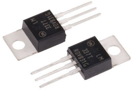
| 产品图片 |
|
| rohs | 符合RoHS无铅 / 符合限制有害物质指令(RoHS)规范要求 |
| 产品系列 | 电源管理 IC,线性稳压器,ON Semiconductor LM337TG- |
| 数据手册 | |
| 产品型号 | LM337TG |
| PSRR/纹波抑制—典型值 | 77 dB |
| 产品目录页面 | |
| 产品种类 | |
| 供应商器件封装 | TO-220AB |
| 其它名称 | LM337TGOS |
| 包装 | 管件 |
| 商标 | ON Semiconductor |
| 安装类型 | 通孔 |
| 安装风格 | Through Hole |
| 封装 | Tube |
| 封装/外壳 | TO-220-3 |
| 封装/箱体 | TO-220-3 |
| 工作温度 | 0°C ~ 125°C |
| 工厂包装数量 | 50 |
| 最大工作温度 | + 125 C |
| 最大输入电压 | - 40 V |
| 最小工作温度 | 0 C |
| 最小输入电压 | - 4.2 V |
| 极性 | Negative |
| 标准包装 | 50 |
| 电压-跌落(典型值) | - |
| 电压-输入 | 可下调至 -40V |
| 电压-输出 | -1.2 V ~ -37 V |
| 电流-输出 | 1.5A |
| 电流-限制(最小值) | - |
| 稳压器拓扑 | 负,可调式 |
| 稳压器数 | 1 |
| 系列 | LM337 |
| 线路调整率 | 0.04 % / V |
| 负载调节 | 1 % / V |
| 输出电压 | - 1.2 V to - 37 V |
| 输出电流 | 1.5 A |
| 输出端数量 | 1 |
| 输出类型 | Adjustable |


- 商务部:美国ITC正式对集成电路等产品启动337调查
- 曝三星4nm工艺存在良率问题 高通将骁龙8 Gen1或转产台积电
- 太阳诱电将投资9.5亿元在常州建新厂生产MLCC 预计2023年完工
- 英特尔发布欧洲新工厂建设计划 深化IDM 2.0 战略
- 台积电先进制程称霸业界 有大客户加持明年业绩稳了
- 达到5530亿美元!SIA预计今年全球半导体销售额将创下新高
- 英特尔拟将自动驾驶子公司Mobileye上市 估值或超500亿美元
- 三星加码芯片和SET,合并消费电子和移动部门,撤换高东真等 CEO
- 三星电子宣布重大人事变动 还合并消费电子和移动部门
- 海关总署:前11个月进口集成电路产品价值2.52万亿元 增长14.8%


PDF Datasheet 数据手册内容提取
LM337 1.5 A, Adjustable Output, Negative Voltage Regulator The LM337 is an adjustable 3−terminal negative voltage regulator capable of supplying in excess of 1.5 A over an output voltage range of −1.2V to −37 V. This voltage regulator is exceptionally easy to use and requires only two external resistors to set the output voltage. www.onsemi.com Further, it employs internal current limiting, thermal shutdown and safe area compensation, making it essentially blow−out proof. The LM337 serves a wide variety of applications including local, on THREE−TERMINAL card regulation. This device can also be used to make a programmable ADJUSTABLE NEGATIVE output regulator, or by connecting a fixed resistor between the VOLTAGE REGULATOR adjustment and output, the LM337 can be used as a precision current regulator. MARKING Features DIAGRAMS • Output Current in Excess of 1.5 A • Output Adjustable between −1.2 V and −37 V • Internal Thermal Overload Protection LM • Internal Short Circuit Current Limiting Constant with Temperature D2PAK 337yyyy • Output Transistor Safe−Area Compensation D2T SUFFIX AWLYWWG CASE 936 • Floating Operation for High Voltage Applications • Eliminates Stocking many Fixed Voltages • Available in Surface Mount D2PAK and Standard 3−Lead Transistor Heatsink surface (shown as terminal 4 in Package case outline drawing) is connected to Pin 2. • These Devices are Pb−Free and are RoHS Compliant Pin 1. Adjust 2. Vin 3. Vout IPROG + R2 + Cin* CO** 1.0 (cid:2)F R1 1.0 (cid:2)F TO−220AB 120 T SUFFIX CASE 221AB IAdj LM Heatsink surface 337xx connected to Pin 2. AWLYWWG Vin Vout -Vin LM337 -Vout 1 *(cid:3)Cin is required if regulator is located more than 4 inches from power supply filter. xx = BT, T *(cid:3)A 1.0 (cid:2)F solid tantalum or 10 (cid:2)F aluminum electrolytic is recommended. yyyy = BD2T, D2T **(cid:3)CO is necessary for stability. A 1.0 (cid:2)F solid tantalum or 10 (cid:2)F aluminum electrolytic AWL == WAsasfeemr Lbolyt Location **(cid:3)is recommended. (cid:3) (cid:5) Y = Year V (cid:2)(cid:2)(cid:2)–1.25(cid:2)V(cid:2) 1(cid:4)R2 WW = Work Week out R G = Pb−Free Package 1 Figure 1. Standard Application ORDERING INFORMATION See detailed ordering and shipping information in the package dimensions section on page 9 of this data sheet. © Semiconductor Components Industries, LLC, 2015 1 Publication Order Number: January, 2015 − Rev. 10 LM337/D
LM337 MAXIMUM RATINGS (TA = +25°C, unless otherwise noted) Rating Symbol Value Unit Input−Output Voltage Differential VI−VO 40 Vdc Power Dissipation Case 221A TA = +25°C PD Internally Limited W Thermal Resistance, Junction−to−Ambient (cid:3) 65 °C/W JA Thermal Resistance, Junction−to−Case (cid:3) 5.0 °C/W JC Case 936 (D2PAK) TA = +25°C PD Internally Limited W Thermal Resistance, Junction−to−Ambient (cid:3) 70 °C/W JA Thermal Resistance, Junction−to−Case (cid:3) 5.0 °C/W JC Operating Junction Temperature Range TJ −40 to +125 °C Storage Temperature Range Tstg −65 to +150 °C Stresses exceeding those listed in the Maximum Ratings table may damage the device. If any of these limits are exceeded, device functionality should not be assumed, damage may occur and reliability may be affected. ELECTRICAL CHARACTERISTICS (|VI−VO| = 5.0 V; IO = 0.5 A for T package; TJ = Tlow to Thigh [Note 1]; Imax and Pmax [Note 2].) Characteristics Figure Symbol Min Typ Max Unit Line Regulation (Note 3), TA = +25°C, 3.0 V ≤ |VI−VO| ≤ 40 V 1 Regline − 0.01 0.04 %/V Load Regulation (Note 3), TA = +25°C, 10 mA ≤ IO ≤ Imax 2 Regload |VO| ≤ 5.0 V − 15 50 mV |VO| ≥ 5.0 V − 0.3 1.0 % VO Thermal Regulation, TA = +25°C (Note 5), 10 ms Pulse Regtherm − 0.003 0.04 % VO/W Adjustment Pin Current 3 IAdj − 65 100 (cid:2)A Adjustment Pin Current Change, 2.5 V ≤ |VI−VO| ≤ 40 V, 1, 2 (cid:4)IAdj − 2.0 5.0 (cid:2)A 10 mA ≤ IL ≤ Imax, PD ≤ Pmax, TA = +25°C Reference Voltage, TA = +25°C, 3.0 V ≤ |VI−VO| ≤ 40 V, 3 Vref −1.213 −1.250 −1.287 V 10 mA ≤ IO ≤ Imax, PD ≤ Pmax, TJ = Tlow to Thigh −1.20 −1.25 −1.30 Line Regulation (Note 3), 3.0 V ≤ |VI−VO| ≤ 40 V 1 Regline − 0.02 0.07 %/V Load Regulation (Note 3), 10 mA ≤ IO ≤ Imax 2 Regload |VO| ≤ 5.0 V − 20 70 mV |VO| ≥ 5.0 V − 0.3 1.5 % VO Temperature Stability (Tlow ≤ TJ ≤ Thigh) 3 TS − 0.6 − % VO Minimum Load Current to Maintain Regulation 3 ILmin mA (|VI−VO| ≤ 10 V) − 1.5 6.0 (|VI−VO| ≤ 40 V) − 2.5 10 Maximum Output Current 3 Imax A |VI−VO| ≤ 15 V, PD ≤ Pmax, T Package − 1.5 2.2 |VI−VO| ≤ 40 V, PD ≤ Pmax, TJ = +25°C, T Package − 0.15 0.4 RMS Noise, % of VO, TA = +25°C, 10 Hz ≤ f ≤ 10 kHz N − 0.003 − % VO Ripple Rejection, VO = −10 V, f = 120 Hz (Note 4) 4 RR dB Without CAdj − 60 − CAdj = 10 (cid:2)F 66 77 − Long−Term Stability, TJ = Thigh (Note 6), TA = +25°C for 3 S − 0.3 1.0 %/1.0 k Endpoint Measurements Hrs. Thermal Resistance, Junction−to−Case, T Package R(cid:3)JC − 4.0 − °C/W Product parametric performance is indicated in the Electrical Characteristics for the listed test conditions, unless otherwise noted. Product performance may not be indicated by the Electrical Characteristics if operated under different conditions. 1. Tlow to Thigh = 0° to +125°C, for LM337T, D2T. Tlow to Thigh = −40° to +125°C, for LM337BT, BD2T. 2. Imax = 1.5 A, Pmax = 20 W 3. Load and line regulation are specified at constant junction temperature. Change in VO because of heating effects is covered under the Thermal Regulation specification. Pulse testing with a low duty cycle is used. 4. CAdj, when used, is connected between the adjustment pin and ground. 5. Power dissipation within an IC voltage regulator produces a temperature gradient on the die, affecting individual IC components on the die. These effects can be minimized by proper integrated circuit design and layout techniques. Thermal Regulation is the effect of these temperature gradients on the output voltage and is expressed in percentage of output change per watt of power change in a specified time. 6. Since Long Term Stability cannot be measured on each device before shipment, this specification is an engineering estimate of average stability from lot to lot. www.onsemi.com 2
LM337 Representative Schematic Diagram Adjust 100 60 2.0k 2.5k 810 21k Vout 10k 800 15pF 25pF 5.0k 220 75 60k 100k 800 15pF 2.0k 0 18k 4.0k 6.0k 100 1.0k 3.0k 2.2k 18k 9.6k 30k 270 2.0 100pF 5.0pF 240 pF 250 20k 8.0k 5.0k 0.2 600 100k 15 2.9k 4.0k 155 500 2.4k 15 500 0.05 Vin This device contains 39 active transistors. R2 1% + Cin 1.0 (cid:2)F IAdj CO 1.0 (cid:2)F 120 *(cid:2)Pulse testing required. Adjust R1 1% RL (cid:4)(cid:2)1% Duty Cycle (cid:4)(cid:2)is suggested. Vin Vout LM337 VIH VOH * VIL VOL |V –V | OL OH VEE Line(cid:2)Regulation(cid:2)(%(cid:6)V)(cid:2)(cid:2)(cid:2) |V | x(cid:2)100 OH Figure 1. Line Regulation and (cid:4)I /Line Test Circuit Adj www.onsemi.com 3
LM337 *(cid:2)Pulse testing required. R2 1% (cid:4)(cid:2)1% Duty Cycle is suggested. CO + Cin 1.0 (cid:2)F 1.0 (cid:2)F IAdj R1 120 Adjust * RL (max Vin Vout Load) -VO (min Load) -VI LM337 IL -VO (max Load) VO (min Load) - VO (max Load) Load Regulation (mV) = VO (min Load) - VO (max Load) Load Regulation (% VO) = VO (min Load) x 100 Figure 2. Load Regulation and (cid:4)I /Load Test Circuit Adj R2 1% + VI Cin 1.0 (cid:2)F CO 1.0 (cid:2)F RL VO IAdj Vref R1 120 Adjust Vin Vout LM337 IL VO To Calculate R2: R2 = - 1 R1 Vref * Pulse testing required. This assumes IAdj is negligible. * 1% Duty Cycle is suggested. Figure 3. Standard Test Circuit + R2 1% CAdj 10(cid:2)F + Cin 1.0 (cid:2)F CO 1.0 (cid:2)F RL VO Adjust R1 120 D1* 1N4002 Vin Vout LM337 Vout = -1.25 V 14.3 V 4.3 V * D1 Discharges CAdj if output is shorted to Ground. f = 120 Hz Figure 4. Ripple Rejection Test Circuit www.onsemi.com 4
LM337 0.2 4.0 %) E ( 0 HANG -0.2 IL = 0.5 A T (A) 3.0 C N GE -0.4 RE A R T U , OUTPUT VOLout ----0011....6802 VVoinu =t = - -1150 V V IL = 1.5 A I, OUTPUT Cout21..00 TJ = 25°C V Δ -1.4 0 -50 -25 0 25 50 75 100 125 150 0 10 20 30 40 TJ, JUNCTION TEMPERATURE (°C) Vin-Vout , INPUT-OUTPUT VOLTAGE DIFFERENTIAL (Vdc) Figure 5. Load Regulation Figure 6. Current Limit 80 3.0 E μT (A) 75 OLTAG V(cid:4)oVutO = = - 150.00 VmV NT CURREN 766050 -OUTPUT V NTIAL (Vdc)22..50 IL = 1.5 A ME UT RE 1.0 A ST 55 NP FE DJU 50 , IutDIF1.5 500 mA A o , Adj 45 - Vn 200 mA I Vi 20 mA 40 1.0 -50 -25 0 25 50 75 100 125 150 -50 -25 0 25 50 75 100 125 150 TJ, JUNCTION TEMPERATURE (°C) TJ, JUNCTION TEMPERATURE (°C) Figure 7. Adjustment Pin Current Figure 8. Dropout Voltage 1.27 1.8 V) A) GE ( 1.26 T (m 1.6 TA EN 1.4 L R VO UR 1.2 E C NC 1.25 NT 1.0 TJ = 25°C E E R C 0.8 E S V, REFref1.24 , QUIEIB000...642 1.23 0 -50 -25 0 25 50 75 100 125 150 0 10 20 30 40 TJ, JUNCTION TEMPERATURE (°C) Vin-Vout , INPUT-OUTPUT VOLTAGE DIFFERENTIAL (Vdc) Figure 9. Temperature Stability Figure 10. Minimum Operating Current www.onsemi.com 5
LM337 100 100 RR, RIPPLE REJECTION (dB) 86420000 VIfL =i n= 1- 52 V000o Hu mtz =A 5.0 V WCAitdhj o=u 1t 0C A(cid:2)dFj RR, RIPPLE REJECTION (dB) 86420000 VVf =oinu 1t= 2= -0 -1 H150z V V WCAitdhj o=u 1t 0C (cid:2)AdFj TJ = 25°C TJ = 25°C 0 0 0 -5.0 -10 -15 -20 -25 -30 -35 -40 0.01 0.1 1.0 10 Vout, OUTPUT VOLTAGE (V) IO, OUTPUT CURRENT (A) Figure 11. Ripple Rejection versus Output Voltage Figure 12. Ripple Rejection versus Output Current 100 101 TION (dB) 80 CAdj =10 (cid:2)F VVITLJoi n= u =t= 5 = 20- 5-10°15 Cm0 V AV ΩNCE ((cid:5)) 100 VVICLoiL n=u =t= 5= 10- .-10015 m(cid:2)0 V FAV EC 60 DA TJ = 25°C REJ MPE 10-1 LE T I Without CAdj PP 40 Without CAdj PU RR, RI 20 , OUTO10-2 CAdj = 10 (cid:2)F Z 0 10-3 10 100 1.0 k 10 k 100 k 1.0 M 10 M 10 100 1.0 k 10 k 100 k 1.0 M f, FREQUENCY (Hz) f, FREQUENCY (Hz) Figure 13. Ripple Rejection versus Frequency Figure 14. Output Impedance ΔV, OUTPUToutVOLTAGE DEVIATION (V) 0000....86402 Without CAdj ΔV, OUTPUToutVOLTAGE DEVIATION (V)--00000.....642024 CAdj = 10 W(cid:2)Fithout CAdj V)-0.2 CAdj = 10 (cid:2)F -0.6 ΔV, INPUTinAGE CHANGE (--00..504 CVITLJoL = u ==t 5 = 210 5.- 0m°1 C(cid:2)0A FV I, LOADLURRENT (A)--01..500 VTVICLJoiL n= u ===t 5 = 21-0 5.-1 0m°15 C(cid:2)0 AV FV LT-1.0 C-1.5 O 0 10 20 30 40 0 10 20 30 40 V t, TIME ((cid:2)s) t, TIME ((cid:2)s) Figure 15. Line Transient Response Figure 16. Load Transient Response www.onsemi.com 6
LM337 APPLICATIONS INFORMATION Basic Circuit Operation The LM337 is a 3−terminal floating regulator. In External Capacitors operation, the LM337 develops and maintains a nominal A 1.0 (cid:2)F tantalum input bypass capacitor (C ) is in −1.25 V reference (Vref) between its output and adjustment recommended to reduce the sensitivity to input line terminals. This reference voltage is converted to a impedance. programming current (IPROG) by R1 (see Figure 17), and this The adjustment terminal may be bypassed to ground to constant current flows through R2 from ground. improve ripple rejection. This capacitor (CAdj) prevents The regulated output voltage is given by: ripple from being amplified as the output voltage is (cid:3) (cid:5) increased. A 10(cid:2)F capacitor should improve ripple R V (cid:2)(cid:2)(cid:2)V (cid:2) 1(cid:4) 2 (cid:2)(cid:4)(cid:2)I (cid:2)R rejection about 15 dB at 120 Hz in a 10 V application. out ref R Adj 2 1 An output capacitance (C ) in the form of a 1.0 (cid:2)F O Since the current into the adjustment terminal (I ) tantalum or 10 (cid:2)F aluminum electrolytic capacitor is Adj represents an error term in the equation, the LM337 was required for stability. Using the classical tantalum or designed to control I to less than 100 (cid:2)A and keep it aluminum electrolytic capacitor types with non−reduced Adj constant. To do this, all quiescent operating current is ESR (Equivalent Series Resistance) value is necessary. returned to the output terminal. This imposes the Low−ESR or similar capacitor types with reduced ESR requirement for a minimum load current. If the load current value and ceramic capacitors can cause instability or is less than this minimum, the output voltage will rise. continuous oscillations in the application. Since the LM337 is a floating regulator, it is only the Protection Diodes voltage differential across the circuit which is important to When external capacitors are used with any IC regulator performance, and operation at high voltages with respect to it is sometimes necessary to add protection diodes to prevent ground is possible. the capacitors from discharging through low current points +Vout into the regulator. Figure 18 shows the LM337 with the recommended R2 protection diodes for output voltages in excess of −25 V or IAdj IPROG + high capacitance values (CO > 25 (cid:2)F, CAdj > 10 (cid:2)F). Diode CO D1 prevents CO from discharging thru the IC during an input short circuit. Diode D protects against capacitor C Adjust Vref R1 discharging through the2 IC during an output short circuAidt.j The combination of diodes D and D prevents C from 1 2 Adj Vin LM337 -Vout the discharging through the IC during an input short circuit. Vout Vref = -1.25 V Typical + +Vout Figure 17. Basic Circuit Configuration R2 CAdj + + Load Regulation Cin CO The LM337 is capable of providing extremely good load Adjust R1 D2 regulation, but a few precautions are needed to obtain 1N4002 -Vin LM337 -Vout maximum performance. For best performance, the Vin Vout programming resistor (R ) should be connected as close to 1 the regulator as possible to minimize line drops which D1 effectively appear in series with the reference, thereby 1N4002 degrading regulation. The ground end of R can be returned 2 Figure 18. Voltage Regulator with Protection Diodes near the load ground to provide remote ground sensing and improve load regulation. www.onsemi.com 7
LM337 80 3.5 W) PD(max) for TA = +50°C N ( E O , THERMAL RESISTANCθJA°JUNCTION‐TO‐AIR ( C/W) 45670000 VMFeroeruteicn aAtelildry MSiizneim Puamd LÎÎÎÎ2.0 oÎÎÎÎz. CLoÎÎÎÎpperÎÎÎÎ2123....5500 AXIMUM POWER DISSIPATI R M R(cid:3)JA , D P 30 1.0 0 5.0 10 15 20 25 30 L, LENGTH OF COPPER (mm) Figure 19. D2PAK Thermal Resistance and Maximum Power Dissipation versus P.C.B. Copper Length www.onsemi.com 8
LM337 ORDERING INFORMATION Device Operating Temperature Range Package Shipping† LM337BD2TG D2PAK 50 Units / Rail (Pb−Free) LM337BD2TR4G D2PAK TJ = −40° to +125°C (Pb−Free) 800 / Tape & Reel LM337BTG TO−220AB (Pb−Free) 50 Units / Rail LM337D2TG D2PAK (Pb−Free) LM337D2TR4G D2PAK TJ = 0° to +125°C (Pb−Free) 800 / Tape & Reel LM337TG TO−220AB 50 Units / Rail (Pb−Free) †For information on tape and reel specifications, including part orientation and tape sizes, please refer to our Tape and Reel Packaging Specifications Brochure, BRD8011/D. www.onsemi.com 9
LM337 PACKAGE DIMENSIONS D2PAK CASE 936−03 ISSUE D NOTES: T T (cid:5)(cid:4)1. DIMENSIONING AND TOLERANCING PER ANSI TERMINAL 4 Y14.5M, 1982. C C K A OCHPATIMOFNEARL ED U OCHPATIMOFNEARL ES (cid:5)(cid:5)(cid:4)(cid:4)23..DIMCTEAONBNS CTIORONONSLT LOAINU AGRN DOD IPKMT.EIONNSAIOLN W: IINTHCIHNES. (cid:5)(cid:4)4. DIMENSIONS U AND V ESTABLISH A MINIMUM S MOUNTING SURFACE FOR TERMINAL 4. V (cid:5)(cid:4)5. DIMENSIONS A AND B DO NOT INCLUDE B MOLD FLASH OR GATE PROTRUSIONS. MOLD H DETAIL C DETAIL C FLASH AND GATE PROTRUSIONS NOT TO 1 2 3 EXCEED 0.025 (0.635) MAXIMUM. (cid:5)(cid:4)6. SINGLE GAUGE DESIGN WILL BE SHIPPED AFTER FPCN EXPIRATION IN OCTOBER 2011. J INCHES MILLIMETERS F SIDE VIEW BOTTOM VIEW SIDE VIEW DIM MIN MAX MIN MAX G DUAL GAUGE SINGLE GAUGE A 0.386 0.403 9.804 10.236 2XD CONSTRUCTION CONSTRUCTION B 0.356 0.368 9.042 9.347 C 0.170 0.180 4.318 4.572 0.010 (0.254) M T D 0.026 0.036 0.660 0.914 TOP VIEW ED 0.045 0.055 1.143 1.397 ES 0.018 0.026 0.457 0.660 F 0.051 REF 1.295 REF G 0.100 BSC 2.540 BSC H 0.539 0.579 13.691 14.707 N T J 0.125 MAX 3.175 MAX M K 0.050 REF 1.270 REF L 0.000 0.010 0.000 0.254 M 0.088 0.102 2.235 2.591 SEATING N 0.018 0.026 0.457 0.660 P L PLANE P 0.058 0.078 1.473 1.981 R 5 (cid:2) REF 5 (cid:2) REF R DETAIL C BOTTOM VIEW S 0.116 REF 2.946 REF OPTIONAL CONSTRUCTIONS U 0.200 MIN 5.080 MIN V 0.250 MIN 6.350 MIN SOLDERING FOOTPRINT* 10.49 8.38 16.155 2X 3.504 2X 1.016 5.080 PITCH DIMENSIONS: MILLIMETERS *For additional information on our Pb−Free strategy and soldering details, please download the ON Semiconductor Soldering and Mounting Techniques Reference Manual, SOLDERRM/D. www.onsemi.com 10
LM337 PACKAGE DIMENSIONS TO−220, SINGLE GAUGE CASE 221AB ISSUE A NOTES: 1. DIMENSIONING AND TOLERANCING PER ANSI Y14.5M, 1982. −T− SPELAATNIENG 23.. CDOIMNETNRSOIOLLNI NZG D DEFIMINEENSS IAO ZNO: INNEC WHEHSE.RE ALL BODY AND B F C LEAD IRREGULARITIES ARE ALLOWED. 4. PRODUCT SHIPPED PRIOR TO 2008 HAD DIMENSIONS T S S = 0.045 - 0.055 INCHES (1.143 - 1.397 MM) 4 INCHES MILLIMETERS DIM MIN MAX MIN MAX Q A A 0.570 0.620 14.48 15.75 B 0.380 0.405 9.66 10.28 C 0.160 0.190 4.07 4.82 1 2 3 U D 0.025 0.035 0.64 0.88 H F 0.142 0.147 3.61 3.73 G 0.095 0.105 2.42 2.66 K H 0.110 0.155 2.80 3.93 Z J 0.018 0.025 0.46 0.64 K 0.500 0.562 12.70 14.27 L 0.045 0.060 1.15 1.52 N 0.190 0.210 4.83 5.33 L R Q 0.100 0.120 2.54 3.04 V J R 0.080 0.110 2.04 2.79 S 0.020 0.024 0.508 0.61 G T 0.235 0.255 5.97 6.47 U 0.000 0.050 0.00 1.27 D V 0.045 --- 1.15 --- N Z --- 0.080 --- 2.04 ON Semiconductor and the are registered trademarks of Semiconductor Components Industries, LLC (SCILLC) or its subsidiaries in the United States and/or other countries. SCILLC owns the rights to a number of patents, trademarks, copyrights, trade secrets, and other intellectual property. A listing of SCILLC’s product/patent coverage may be accessed at www.onsemi.com/site/pdf/Patent−Marking.pdf. SCILLC reserves the right to make changes without further notice to any products herein. SCILLC makes no warranty, representation or guarantee regarding the suitability of its products for any particular purpose, nor does SCILLC assume any liability arising out of the application or use of any product or circuit, and specifically disclaims any and all liability, including without limitation special, consequential or incidental damages. “Typical” parameters which may be provided in SCILLC data sheets and/or specifications can and do vary in different applications and actual performance may vary over time. All operating parameters, including “Typicals” must be validated for each customer application by customer’s technical experts. SCILLC does not convey any license under its patent rights nor the rights of others. SCILLC products are not designed, intended, or authorized for use as components in systems intended for surgical implant into the body, or other applications intended to support or sustain life, or for any other application in which the failure of the SCILLC product could create a situation where personal injury or death may occur. Should Buyer purchase or use SCILLC products for any such unintended or unauthorized application, Buyer shall indemnify and hold SCILLC and its officers, employees, subsidiaries, affiliates, and distributors harmless against all claims, costs, damages, and expenses, and reasonable attorney fees arising out of, directly or indirectly, any claim of personal injury or death associated with such unintended or unauthorized use, even if such claim alleges that SCILLC was negligent regarding the design or manufacture of the part. SCILLC is an Equal Opportunity/Affirmative Action Employer. This literature is subject to all applicable copyright laws and is not for resale in any manner. PUBLICATION ORDERING INFORMATION LITERATURE FULFILLMENT: N. American Technical Support: 800−282−9855 Toll Free ON Semiconductor Website: www.onsemi.com Literature Distribution Center for ON Semiconductor USA/Canada P.O. Box 5163, Denver, Colorado 80217 USA Europe, Middle East and Africa Technical Support: Order Literature: http://www.onsemi.com/orderlit Phone: 303−675−2175 or 800−344−3860 Toll Free USA/Canada Phone: 421 33 790 2910 Fax: 303−675−2176 or 800−344−3867 Toll Free USA/Canada Japan Customer Focus Center For additional information, please contact your local Email: orderlit@onsemi.com Phone: 81−3−5817−1050 Sales Representative www.onsemi.com LM337/D 11
Mouser Electronics Authorized Distributor Click to View Pricing, Inventory, Delivery & Lifecycle Information: O N Semiconductor: LM337BD2TG LM337BD2TR4G LM337BTG LM337D2TG LM337D2TR4G LM337TG