ICGOO在线商城 > 集成电路(IC) > PMIC - 稳压器 - 线性 > LM7912CT
/LM7912CT.jpg)
 Datasheet下载
- 型号: LM7912CT
- 制造商: Fairchild Semiconductor
- 库位|库存: xxxx|xxxx
- 要求:
| 数量阶梯 | 香港交货 | 国内含税 |
| +xxxx | $xxxx | ¥xxxx |
查看当月历史价格
查看今年历史价格
LM7912CT产品简介:
ICGOO电子元器件商城为您提供LM7912CT由Fairchild Semiconductor设计生产,在icgoo商城现货销售,并且可以通过原厂、代理商等渠道进行代购。 LM7912CT价格参考¥4.33-¥5.41。Fairchild SemiconductorLM7912CT封装/规格:PMIC - 稳压器 - 线性, Linear Voltage Regulator IC Negative Fixed 1 Output -12V 1.5A TO-220-3。您可以下载LM7912CT参考资料、Datasheet数据手册功能说明书,资料中有LM7912CT 详细功能的应用电路图电压和使用方法及教程。
Texas Instruments(德州仪器)的LM7912CT是一款线性稳压器,属于PMIC(电源管理集成电路)类别。它主要用于提供稳定的负电压输出,具体为-12V。这款稳压器适用于需要稳定负电压供电的各种应用场景,尤其在模拟电路、通信设备、工业控制和消费电子等领域中表现优异。

 应用场景

1. 模拟电路:
   - 在音频放大器、滤波器等模拟电路中,通常需要正负对称的电源供电。LM7912CT可以提供稳定的-12V输出,与正电压稳压器(如LM7812)配合使用,确保电路工作在理想的电压范围内,减少噪声和失真。

2. 通信设备:
   - 通信设备中的接收器、发射器和其他信号处理模块可能需要负电压来偏置某些关键元件。LM7912CT可以为这些模块提供稳定的-12V电源,确保信号的完整性和可靠性。

3. 工业控制:
   - 工业控制系统中的传感器、执行器和数据采集模块可能需要负电压供电。LM7912CT能够为这些模块提供稳定的电源,确保系统的正常运行,特别是在恶劣的工业环境中,其良好的热特性和稳定性尤为重要。

4. 消费电子产品:
   - 在一些高端消费电子产品中,如音响设备、视频处理设备等,可能需要负电压来驱动特定的电路部分。LM7912CT可以为这些设备提供可靠的电源支持,确保产品性能稳定。

5. 实验室和测试设备:
   - 实验室中的各种测试仪器,如示波器、信号发生器等,通常需要精确的负电压源。LM7912CT可以作为这些设备的负电压源,提供高精度和低噪声的电源,确保测量结果的准确性。

 特点

- 低功耗:LM7912CT具有较低的静态电流,适合用于对功耗敏感的应用。
- 过载保护:内置过流保护和过热关断功能,确保在异常情况下不会损坏芯片或负载。
- 简单易用:只需要少量外部元件即可实现稳定的负电压输出,设计简单,便于集成到各种电路中。

综上所述,LM7912CT凭借其稳定的负电压输出、低功耗和保护功能,广泛应用于多种需要负电压供电的场景中,确保系统稳定可靠运行。
| 参数 | 数值 |
| 产品目录 | 集成电路 (IC)半导体 |
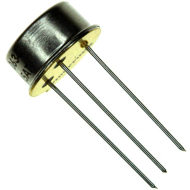
| 描述 | IC REG LDO -12V 1A TO220-3线性稳压器 3-Term 1A Negative Voltage Regulator |
| 产品分类 | |
| 品牌 | Fairchild Semiconductor |
| 产品手册 | |
| 产品图片 |
|
| rohs | 符合RoHS无铅 / 符合限制有害物质指令(RoHS)规范要求 |
| 产品系列 | 电源管理 IC,线性稳压器,Fairchild Semiconductor LM7912CT- |
| 数据手册 | |
| 产品型号 | LM7912CT |
| PCN设计/规格 | |
| PSRR/纹波抑制—典型值 | 60 dB |
| 产品目录页面 | |
| 产品种类 | |
| 供应商器件封装 | TO-220-3 |
| 其它名称 | LM7912CTFS |
| 包装 | 管件 |
| 单位重量 | 1.214 g |
| 商标 | Fairchild Semiconductor |
| 安装类型 | 通孔 |
| 安装风格 | Through Hole |
| 封装 | Tube |
| 封装/外壳 | TO-220-3 |
| 封装/箱体 | TO-220-3 |
| 工作温度 | 0°C ~ 125°C |
| 工厂包装数量 | 50 |
| 最大工作温度 | + 125 C |
| 最大输入电压 | - 30 V |
| 最小工作温度 | 0 C |
| 最小输入电压 | - 14.5 V |
| 极性 | Negative |
| 标准包装 | 50 |
| 电压-跌落(典型值) | 2V @ 1A |
| 电压-输入 | 可下调至 -35V |
| 电压-输出 | -12V |
| 电流-输出 | 1A |
| 电流-限制(最小值) | - |
| 稳压器拓扑 | 负,固定式 |
| 稳压器数 | 1 |
| 系列 | LM79 |
| 线路调整率 | 240 mV |
| 负载调节 | 240 mV |
| 输出电压 | - 12 V |
| 输出电流 | 1 A |
| 输出端数量 | 1 |
| 输出类型 | Fixed |


- 商务部:美国ITC正式对集成电路等产品启动337调查
- 曝三星4nm工艺存在良率问题 高通将骁龙8 Gen1或转产台积电
- 太阳诱电将投资9.5亿元在常州建新厂生产MLCC 预计2023年完工
- 英特尔发布欧洲新工厂建设计划 深化IDM 2.0 战略
- 台积电先进制程称霸业界 有大客户加持明年业绩稳了
- 达到5530亿美元!SIA预计今年全球半导体销售额将创下新高
- 英特尔拟将自动驾驶子公司Mobileye上市 估值或超500亿美元
- 三星加码芯片和SET,合并消费电子和移动部门,撤换高东真等 CEO
- 三星电子宣布重大人事变动 还合并消费电子和移动部门
- 海关总署:前11个月进口集成电路产品价值2.52万亿元 增长14.8%


PDF Datasheet 数据手册内容提取
Is Now Part of To learn more about ON Semiconductor, please visit our website at www.onsemi.com Please note: As part of the Fairchild Semiconductor integration, some of the Fairchild orderable part numbers will need to change in order to meet ON Semiconductor’s system requirements. Since the ON Semiconductor product management systems do not have the ability to manage part nomenclature that utilizes an underscore (_), the underscore (_) in the Fairchild part numbers will be changed to a dash (-). This document may contain device numbers with an underscore (_). Please check the ON Semiconductor website to verify the updated device numbers. The most current and up-to-date ordering information can be found at www.onsemi.com. Please email any questions regarding the system integration to Fairchild_questions@onsemi.com. ON Semiconductor and the ON Semiconductor logo are trademarks of Semiconductor Components Industries, LLC dba ON Semiconductor or its subsidiaries in the United States and/or other countries. ON Semiconductor owns the rights to a number of patents, trademarks, copyrights, trade secrets, and other intellectual property. A listing of ON Semiconductor’s product/patent coverage may be accessed at www.onsemi.com/site/pdf/Patent-Marking.pdf. ON Semiconductor reserves the right to make changes without further notice to any products herein. ON Semiconductor makes no warranty, representation or guarantee regarding the suitability of its products for any particular purpose, nor does ON Semiconductor assume any liability arising out of the application or use of any product or circuit, and specifically disclaims any and all liability, including without limitation special, consequential or incidental damages. Buyer is responsible for its products and applications using ON Semiconductor products, including compliance with all laws, regulations and safety requirements or standards, regardless of any support or applications information provided by ON Semiconductor. “Typical” parameters which may be provided in ON Semiconductor data sheets and/or specifications can and do vary in different applications and actual performance may vary over time. All operating parameters, including “Typicals” must be validated for each customer application by customer’s technical experts. ON Semiconductor does not convey any license under its patent rights nor the rights of others. ON Semiconductor products are not designed, intended, or authorized for use as a critical component in life support systems or any FDA Class 3 medical devices or medical devices with a same or similar classification in a foreign jurisdiction or any devices intended for implantation in the human body. Should Buyer purchase or use ON Semiconductor products for any such unintended or unauthorized application, Buyer shall indemnify and hold ON Semiconductor and its officers, employees, subsidiaries, affiliates, and distributors harmless against all claims, costs, damages, and expenses, and reasonable attorney fees arising out of, directly or indirectly, any claim of personal injury or death associated with such unintended or unauthorized use, even if such claim alleges that ON Semiconductor was negligent regarding the design or manufacture of the part. ON Semiconductor is an Equal Opportunity/Affirmative Action Employer. This literature is subject to all applicable copyright laws and is not for resale in any manner.
www.fairchildsemi.com LM79XX 3-Terminal 1A Negative Voltage Regulator Features Description • Output Current in Excess of 1A The LM79XX series of three terminal negative regulators • Output Voltages of -5, -6, -8 , -9, -10, -12, -15, -18 and - are available in TO-220 package and with several fixed 24V output voltages, making them useful in a wide range • Internal Thermal Overload Protection of applications. Each type employs internal current limiting, • Short Circuit Protection thermal shut down and safe operating area protection, • Output Transistor Safe Operating Area Compensation making it essentially indestructible. TO-220 (Single Gauge) Vin 1 1. GND 2. Input 3. Output Internal Block Digram GND R1 VOLTAGE REFERENCE R2 OOuutptut + Q1 - Q2 PROTECTION I1 I2 CIRCUITRY Rsc In Input Rev. 1.0.3 ©2011 Fairchild Semiconductor Corporation
LM79XX Absolute Maximum Ratings Parameter Symbol Value Unit Input Voltage VI -35 V Thermal Resistance Junction-Case (Note1) RθJC 5 °C/W Thermal Resistance Junction-Air (Note1, 2) RθJA 65 Operating Temperature Range TOPR 0 ~ +125 °C Storage Temperature Range TSTG -65 ~ +150 °C Note: 1. Thermal resistance test board Size: 76.2mm * 114.3mm * 1.6mm(1S0P) JEDEC standard: JESD51-3, JESD51-7 2. Assume no ambient airflow Electrical Characteristics (LM7905) (VI = -10V, IO = 500mA, 0°C ≤TJ ≤ +125°C, CI =2.2μF, CO =1μF, unless otherwise specified.) Parameter Symbol Conditions Min. Typ. Max. Unit TJ = +25°C -4.8 -5.0 -5.2 Output Voltage VO IO = 5mA to 1A, PO ≤ 15W V -4.75 -5.0 -5.25 VI = -7V to -20V VI = -7V to -25V - 35 100 Line Regulation (Note3) ΔVO TJ = +25°C mV VI = -8V to -12V - 8 50 TJ = +25°C - 10 100 IO = 5mA to 1.5A Load Regulation (Note3) ΔVO mV TJ =+25°C - 3 50 IO = 250mA to 750mA Quiescent Current IQ TJ =+25°C - 3 6 mA IO = 5mA to 1A - 0.05 0.5 Quiescent Current Change ΔIQ mA VI = -8V to -25V - 0.1 0.8 Temperature Coefficient of VD ΔVo/ΔT IO = 5mA - - 0.4 - mV/°C f = 10Hz to 100kHz Output Noise Voltage VN - 40 - μV TA =+25°C f = 120Hz Ripple Rejection RR 54 60 - dB ΔVI = 10V TJ = +25°C Dropout Voltage VD - 2 - V IO = 1A Short Circuit Current ISC TJ =+25°C, VI = -35V - 300 - mA Peak Current IPK TJ =+25°C - 2.2 - A Note 3. Load and line regulation are specified at constant junction temperature. Changes in VO due to heating effects must be taken into account separately. Pulse testing with low duty is used. 2
LM79XX Electrical Characteristics (LM7906) (Continued) (VI = -11V, IO = 500mA, 0°C ≤TJ ≤ +125°C, CI =2.2μF, CO =1μF, unless otherwise specified.) Parameter Symbol Conditions Min. Typ. Max. Unit TJ = +25°C -5.75 -6 -6.25 Output Voltage VO IO = 5mA to 1A, PO ≤ 15W V -5.7 -6 -6.3 VI = -9V to -21V VI = -8V to -25V - 10 120 Line Regulation (Note1) ΔVO TJ = +25°C mV VI = -9V to -13V - 5 60 TJ = +25°C - 10 120 IO = 5mA to 1.5A Load Regulation (Note1) ΔVO mV TJ =+25°C - 3 60 IO = 250mA to 750mA Quiescent Current IQ TJ =+25°C - 3 6 mA IO = 5mA to 1A - 0.05 0.5 Quiescent Current Change ΔIQ mA VI = -8V to -25V - 0.1 1.3 Temperature Coefficient of VD ΔVo/ΔT IO = 5mA - -0.5 - mV/°C f = 10Hz to 100kHz Output Noise Voltage VN - 130 - μV TA =+25°C f = 120Hz Ripple Rejection RR 54 60 - dB ΔVI = 10V TJ = +25°C Dropout Voltage VD - 2 - V IO = 1A Short Circuit Current ISC TJ = +25°C, VI = -35V - 300 - mA Peak Current IPK TJ = +25°C - 2.2 - A Note 1. Load and line regulation are specified at constant junction temperature. Changes in VO due to heating effects must be taken into account separately. Pulse testing with low duty is used. 3
LM79XX Electrical Characteristics (LM7908) (Continued) (VI = -14V, IO = 500mA, 0°C ≤TJ ≤ +125°C, CI =2.2μF, CO =1μF, unless otherwise specified.) Parameter Symbol Conditions Min. Typ. Max. Unit TJ = +25°C -7.7 -8 -8.3 Output Voltage VO IO = 5mA to 1A, PO ≤ 15W V -7.6 -8 -8.4 VI = -10V to -23V VI = -10.5V to -25V - 10 160 Line Regulation (Note1) ΔVO TJ = +25°C mV VI = -11V to -17V - 5 80 TJ = +25°C - 12 160 IO = 5mA to 1.5A Load Regulation (Note1) ΔVO mV TJ =+25°C - 4 80 IO = 250mA to 750mA Quiescent Current IQ TJ =+25°C - 3 6 mA IO = 5mA to 1A - 0.05 0.5 Quiescent Current Change ΔIQ mA VI = -10.5V to -25V - 0.1 1 Temperature Coefficient of VD ΔVo/ΔT IO = 5mA - -0.6 - mV/°C f = 10Hz to 100kHz Output Noise Voltage VN - 175 - μV TA =+25°C f = 120Hz Ripple Rejection RR 54 60 - dB ΔVI = 10V TJ = +25°C Dropout Voltage VD - 2 - V IO = 1A Short Circuit Current ISC TJ = +25°C, VI = -35V - 300 - mA Peak Current IPK TJ = +25°C - 2.2 - A Note 1. Load and line regulation are specified at constant junction temperature. Changes in VO due to heating effects must be taken into account separately. Pulse testing with low duty is used. 4
LM79XX Electrical Characteristics (LM7909) (Continued) (VI = -15V, IO = 500mA, 0°C ≤TJ ≤ +125°C, CI =2.2μF, CO =1μF, unless otherwise specified.) Parameter Symbol Conditions Min. Typ. Max. Unit TJ = +25°C -8.7 -9.0 -9.3 Output Voltage VO IO = 5mA to 1A, PO ≤ 15W V -8.6 -9.0 -9.4 VI = -1.5V to -23V VI = -11.5V to -26V - 10 180 Line Regulation (Note1) ΔVO TJ = +25°C mV VI = -12V to -18V - 5 90 TJ = +25°C - 12 180 IO = 5mA to 1.5A Load Regulation (Note1) ΔVO mV TJ = +25°C - 4 90 IO = 250mA to 750mA Quiescent Current IQ TJ = +25°C - 3 6 mA IO = 5mA to 1A - 0.05 0.5 Quiescent Current Change ΔIQ mA VI = -11.5V to -26V - 0.1 1 Temperature Coefficient of VD ΔVo/ΔT IO = 5mA - -0.6 - mV/°C f = 10Hz to 100kHz Output Noise Voltage VN - 175 - μV TA = +25°C f = 120Hz Ripple Rejection RR 54 60 - dB ΔVI = 10V TJ = +25°C Dropout Voltage VD - 2 - V IO = 1A Short Circuit Current ISC TJ = +25°C, VI = -35V - 300 - mA Peak Current IPK TJ = +25°C - 2.2 - A Note: 1. Load and line regulation are specified at constant junction temperature. Changes in VO due to heating effects must be taken into account separately. Pulse testing with low duty is used. 5
LM79XX Electrical Characteristics (LM7910) (Continued) (VI = -17V, IO = 500mA, 0°C ≤TJ ≤ +125°C, CI =2.2μF, CO =1μF, unless otherwise specified.) Parameter Symbol Conditions Min. Typ. Max. Unit TJ = +25°C -9.6 -10 -10.4 Output Voltage VO IO = 5mA to 1A, Pd ≤ 15W V -9.5 -10 -10.5 VI = -12V to -28 VI = -12.5V to -28V - 12 200 Line Regulation (Note1) ΔVO TJ = +25°C mV VI = -14V to -20V - 6 100 TJ = +25°C - 12 200 IO = 5mA to 1.5A Load Regulation (Note1) ΔVO mV TJ = +25°C - 4 100 IO = 250mA to 750mA Quiescent Current IQ TJ = +25°C - 3 6 mA IO = 5mA to 1A - 0.05 0.5 Quiescent Current Change ΔIQ mA VI = -12.5V to -28V - 0.1 1 Temperature Coefficient of VO ΔVo/ΔT IO = 5mA - -1 - mV/°C 10Hz ≤ f ≤ 100kHz Output Noise Voltage VN - 280 - μV TA =+25°C f = 120Hz Ripple Rejection RR 54 60 - dB ΔVI = 10V TJ = +25°C Dropout Voltage VD - 2 - V IO = 1A Short Circuit Current ISC TJ = +25°C, VI = -35V - 300 - mA Peak Current IPK TJ = +25°C - 2.2 - A Note: 1. Load and line regulation are specified at constant junction temperature. Changes in VO due to heating effects must be taken into account separately. Pulse testing with low duty is used. 6
LM79XX Electrical Characteristics (LM7912) (Continued) (VI = -19V, IO = 500mA, 0°C ≤TJ ≤ +125°C, CI =2.2μF, CO =1μF, unless otherwise specified.) Parameter Symbol Conditions Min. Typ. Max. Unit TJ = +25°C -11.5 -12 -12.5 Output Voltage VO IO = 5mA to 1A, PO ≤ 15W V -11.4 -12 -12.6 VI = -15.5V to -27V VI = -14.5V to -30V - 12 240 Line Regulation (Note1) ΔVO TJ = +25°C mV VI = -16V to -22V - 6 120 TJ = +25°C - 12 240 IO = 5mA to 1.5A Load Regulation (Note1) ΔVO mV TJ = +25°C - 4 120 IO = 250mA to 750mA Quiescent Current IQ TJ = +25°C - 3 6 mA IO = 5mA to 1A - 0.05 0.5 Quiescent Current Change ΔIQ mA VI = -14.5V to -30V - 0.1 1 Temperature Coefficient of VD ΔVo/ΔT IO = 5mA - -0.8 - mV/°C f = 10Hz to 100kHz Output Noise Voltage VN - 200 - μV TA = +25°C f = 120Hz Ripple Rejection RR 54 60 - dB ΔVI = 10V TJ = +25°C Dropout Voltage VD - 2 - V IO = 1A Short Circuit Current ISC TJ = +25°C, VI = -35V - 300 - mA Peak Current IPK TJ = +25°C - 2.2 - A Note: 1. Load and line regulation are specified at constant junction temperature. Changes in VO due to heating effects must be taken into account separately. Pulse testing with low duty is used. 7
LM79XX Electrical Characteristics (LM7915) (Continued) (VI = -23V, IO = 500mA, 0°C ≤TJ ≤ +125°C, CI =2.2μF, CO =1μF, unless otherwise specified.) Parameter Symbol Conditions Min. Typ. Max. Unit TJ = +25°C -14.4 -15 -15.6 Output Voltage VO IO = 5mA to 1A, PO ≤ 15W V -14.25 -15 -15.75 VI = -18V to -30V VI = -17.5V to -30V - 12 300 Line Regulation (Note1) ΔVO TJ = +25°C mV VI = -20V to -26V - 6 150 TJ = +25°C - 12 300 IO = 5mA to 1.5A Load Regulation (Note1) ΔVO mV TJ = +25°C - 4 150 IO = 250mA to 750mA Quiescent Current IQ TJ = +25°C - 3 6 mA IO = 5mA to 1A - 0.05 0.5 Quiescent Current Change ΔIQ mA VI = -17.5V to -30V - 0.1 1 Temperature Coefficient of VD ΔVo/ΔT IO = 5mA - -0.9 - mV/°C f = 10Hz to 100kHz Output Noise Voltage VN - 250 - μV TA =+25°C f = 120Hz Ripple Rejection RR 54 60 - dB ΔVI = 10V TJ = +25°C Dropout Voltage VD - 2 - V IO = 1A Short Circuit Current ISC TJ = +25°C, VI = -35V - 300 - mA Peak Current IPK TJ = +25°C - 2.2 - A Note: 1. Load and line regulation are specified at constant junction temperature. Changes in VO due to heating effects must be taken into account separately. Pulse testing with low duty is used. 8
LM79XX Electrical Characteristics (LM7918) (Continued) (VI = -27V, IO = 500mA, 0°C ≤TJ ≤ +125°C, CI =2.2μF, CO =1μF, unless otherwise specified.) Parameter Symbol Conditions Min. Typ. Max. Unit TJ = +25°C -17.3 -18 -18.7 Output Voltage VO IO = 5mA to 1A, PO ≤ 15W V -17.1 -18 -18.9 VI = -22.5V to -33V VI = -21V to -33V - 15 360 Line Regulation (Note1) ΔVO TJ = +25°C mV VI = -24V to -30V - 8 180 TJ = +25°C - 15 360 IO = 5mA to 1.5A Load Regulation (Note1) ΔVO mV TJ = +25°C - 5 180 IO = 250mA to 750mA Quiescent Current IQ TJ = +25°C - 3 6 mA IO = 5mA to 1A - 0.05 0.5 Quiescent Current Change ΔIQ mA VI = -21V to -33V - 0.1 1 Temperature Coefficient of VD ΔVo/ΔT IO = 5mA - -1 - mV/°C f = 10Hz to 100kHz Output Noise Voltage VN - 300 - μV TA = +25°C f = 120Hz Ripple Rejection RR 54 60 - dB ΔVI = 10V TJ = +25°C Dropout Voltage VD - 2 - V IO = 1A Short Circuit Current ISC TJ = +25°C, VI = -35V - 300 - mA Peak Current IPK TJ = +25°C - 2.2 - A Note: 1. Load and line regulation are specified at constant junction temperature. Changes in VO due to heating effects must be taken into account separately. Pulse testing with low duty is used. 9
LM79XX Electrical Characteristics (LM7924) (Continued) (VI = -33V, IO = 500mA, 0°C ≤TJ ≤ +125°C, CI =2.2μF, CO =1μF, unless otherwise specified.) Parameter Symbol Conditions Min. Typ. Max. Unit TJ = +25°C -23 -24 -25 Output Voltage VO IO = 5mA to 1A, PO ≤ 15W V -22.8 -24 -25.2 VI = -27V to -38V VI = -27V to -38V - 15 480 Line Regulation (Note1) ΔVO TJ = +25°C mV VI = -30V to -36V - 8 180 TJ = +25°C - 15 480 IO = 5mA to 1.5A Load Regulation (Note1) ΔVO mV TJ = +25°C - 5 240 IO = 250mA to 750mA Quiescent Current IQ TJ = +25°C - 3 6 mA IO = 5mA to 1A - 0.05 0.5 Quiescent Current Change ΔIQ mA VI = -27V to -38V - 0.1 1 Temperature Coefficient of VD ΔVo/ΔT IO = 5mA - -1 - mV/°C f = 10Hz to 100kHz Output Noise Voltage VN - 400 - μV TA = +25°C f = 120Hz Ripple Rejection RR 54 60 - dB ΔVI = 10V TJ = +25°C Dropout Voltage VD - 2 - V IO = 1A Short Circuit Current ISC TJ = +25°C, VI = -35V - 300 - mA Peak Current IPK TJ = +25°C - 2.2 - A Note: 1. Load and line regulation are specified at constant junction temperature. Changes in VO due to heating effects must be taken into account separately. Pulse testing with low duty is used. 10
LM79XX Typical Performance Characteristics 5.1 15 Otuge[-V]ptu5.055 VIoi=n=401m0VA on[mV] LaRdoe11139 Io=1.5A Vlg[VOutput Voltat-aeo] 44..489.559 VIoi=n1=0205mVA oad Regulati gao[Vmtun]il-11357 Io=0.75A L -3 4.8 -5 -40 -25 0 25 50 75 100 125 -40 -25 0 25 50 75 100 125 TA, Ambient Temperature [oC] TA, Ambient Temperature [oC] Figure 1.Output Voltage Figure 2.Load Regulation 5 4 A]4.5 3.5 m 4 V] V] 3 Current [23..535 Vl[ Voltage [2.52 nt 2 ut 1.5 e o Io=1A uiesc1.15 D Drop 1 Q 0.5 0.5 0 0 -40 -25 0 25 50 75 100 125 -40 -25 0 25 50 75 100 125 TA, Ambient Temperature [oC] TA, Ambient Temperature [oC] Figure 3.Quiescent Current Figure 4.Dropout Voltage 0.6 0.55 Sh 0.5 ent[A]oCritr0.04.54 Currctui0.03.53 cuit Cu0.02.52 Cirrre0.15 hort n[At]0.00.51 S 0 -0.05 -0.1 -40 -25 0 25 50 75 100 125 TA, Ambient Temperature [oC] Figure 5.Short Circuit Current 11
LM79XX Typical Applications +2.2μF +1μF CI 1 CO 2 3 - VInIput LKMA7799XXXX Outp-u VtO Figure 6.Negative Fixed output regulator 1 3 + 15V MKCA77881122 +12V + + C1 2 Co 1N4001 0.33μF 1μF * GND +2.2μF 1μF + C1 1 Co 1N4001 * 2 3 - 15V LKMA77991122 -12V Figure 7.Split power supply ( ± 12V/1A) Notes: (1) To specify an output voltage, substitute voltage value for "XX " (2) Required for stability. For value given, capacitor must be solid tantalum. If aluminium electronics are used, at least ten times value shown should be selected. CI is required if regulator is located an appreciable distance from power supply filter. (3) To improve transient response. If large capacitors are used, a high current diode from input to output (1N400l or similar) should be introduced to protect the device from momentary input short circuit. 12
LM79XX Mechanical Dimensions Package Dimensions in millimeters TO-220 [ SINGLE GAUGE ] 13
LM79XX Ordering Information Product Number Output Voltage Tolerance Package Operating Temperature LM7905CT LM7906CT LM7908CT LM7909CT TO-220 LM7910CT ±4% 0 ~ +125°C (Single Gauge) LM7912CT LM7915CT LM7918CT LM7924CT 14
LM79XX DISCLAIMER FAIRCHILD SEMICONDUCTOR RESERVES THE RIGHT TO MAKE CHANGES WITHOUT FURTHER NOTICE TO ANY PRODUCTS HEREIN TO IMPROVE RELIABILITY, FUNCTION OR DESIGN. FAIRCHILD DOES NOT ASSUME ANY LIABILITY ARISING OUT OF THE APPLICATION OR USE OF ANY PRODUCT OR CIRCUIT DESCRIBED HEREIN; NEITHER DOES IT CONVEY ANY LICENSE UNDER ITS PATENT RIGHTS, NOR THE RIGHTS OF OTHERS. LIFE SUPPORT POLICY FAIRCHILD’S PRODUCTS ARE NOT AUTHORIZED FOR USE AS CRITICAL COMPONENTS IN LIFE SUPPORT DEVICES OR SYSTEMS WITHOUT THE EXPRESS WRITTEN APPROVAL OF THE PRESIDENT OF FAIRCHILD SEMICONDUCTOR CORPORATION. As used herein: 1. Life support devices or systems are devices or systems 2. A critical component in any component of a life support which, (a) are intended for surgical implant into the body, device or system whose failure to perform can be or (b) support or sustain life, and (c) whose failure to reasonably expected to cause the failure of the life support perform when properly used in accordance with device or system, or to affect its safety or effectiveness. instructions for use provided in the labeling, can be reasonably expected to result in a significant injury of the user. www.fairchildsemi.com 9/7/11 0.0m 001 Stock#DS400021 © 2011 Fairchild Semiconductor Corporation
ON Semiconductor and are trademarks of Semiconductor Components Industries, LLC dba ON Semiconductor or its subsidiaries in the United States and/or other countries. ON Semiconductor owns the rights to a number of patents, trademarks, copyrights, trade secrets, and other intellectual property. A listing of ON Semiconductor’s product/patent coverage may be accessed at www.onsemi.com/site/pdf/Patent−Marking.pdf. ON Semiconductor reserves the right to make changes without further notice to any products herein. ON Semiconductor makes no warranty, representation or guarantee regarding the suitability of its products for any particular purpose, nor does ON Semiconductor assume any liability arising out of the application or use of any product or circuit, and specifically disclaims any and all liability, including without limitation special, consequential or incidental damages. Buyer is responsible for its products and applications using ON Semiconductor products, including compliance with all laws, regulations and safety requirements or standards, regardless of any support or applications information provided by ON Semiconductor. “Typical” parameters which may be provided in ON Semiconductor data sheets and/or specifications can and do vary in different applications and actual performance may vary over time. All operating parameters, including “Typicals” must be validated for each customer application by customer’s technical experts. ON Semiconductor does not convey any license under its patent rights nor the rights of others. ON Semiconductor products are not designed, intended, or authorized for use as a critical component in life support systems or any FDA Class 3 medical devices or medical devices with a same or similar classification in a foreign jurisdiction or any devices intended for implantation in the human body. Should Buyer purchase or use ON Semiconductor products for any such unintended or unauthorized application, Buyer shall indemnify and hold ON Semiconductor and its officers, employees, subsidiaries, affiliates, and distributors harmless against all claims, costs, damages, and expenses, and reasonable attorney fees arising out of, directly or indirectly, any claim of personal injury or death associated with such unintended or unauthorized use, even if such claim alleges that ON Semiconductor was negligent regarding the design or manufacture of the part. ON Semiconductor is an Equal Opportunity/Affirmative Action Employer. This literature is subject to all applicable copyright laws and is not for resale in any manner. PUBLICATION ORDERING INFORMATION LITERATURE FULFILLMENT: N. American Technical Support: 800−282−9855 Toll Free ON Semiconductor Website: www.onsemi.com Literature Distribution Center for ON Semiconductor USA/Canada 19521 E. 32nd Pkwy, Aurora, Colorado 80011 USA Europe, Middle East and Africa Technical Support: Order Literature: http://www.onsemi.com/orderlit Phone: 303−675−2175 or 800−344−3860 Toll Free USA/Canada Phone: 421 33 790 2910 Fax: 303−675−2176 or 800−344−3867 Toll Free USA/Canada Japan Customer Focus Center For additional information, please contact your local Email: orderlit@onsemi.com Phone: 81−3−5817−1050 Sales Representative © Semiconductor Components Industries, LLC www.onsemi.com www.onsemi.com 1
Mouser Electronics Authorized Distributor Click to View Pricing, Inventory, Delivery & Lifecycle Information: O N Semiconductor: LM7912CT