ICGOO在线商城 > 集成电路(IC) > PMIC - 稳压器 - 线性 > TPS76030DBVR
 Datasheet下载
- 型号: TPS76030DBVR
- 制造商: Texas Instruments
- 库位|库存: xxxx|xxxx
- 要求:
| 数量阶梯 | 香港交货 | 国内含税 |
| +xxxx | $xxxx | ¥xxxx |
查看当月历史价格
查看今年历史价格
TPS76030DBVR产品简介:
ICGOO电子元器件商城为您提供TPS76030DBVR由Texas Instruments设计生产,在icgoo商城现货销售,并且可以通过原厂、代理商等渠道进行代购。 TPS76030DBVR价格参考。Texas InstrumentsTPS76030DBVR封装/规格:PMIC - 稳压器 - 线性, Linear Voltage Regulator IC Positive Fixed 1 Output 3V 50mA SOT-23-5。您可以下载TPS76030DBVR参考资料、Datasheet数据手册功能说明书,资料中有TPS76030DBVR 详细功能的应用电路图电压和使用方法及教程。
TPS76030DBVR是德州仪器(Texas Instruments)生产的一款PMIC(电源管理集成电路),具体属于线性稳压器类别。该器件具有低功耗、高精度和小封装的特点,适用于多种需要稳定电压输出的应用场景。

 应用场景:

1. 便携式电子设备:
   TPS76030DBVR的低静态电流(典型值为25µA)使其非常适合用于电池供电的便携式设备,如智能手机、平板电脑、可穿戴设备等。这些设备对电源效率要求较高,而TPS76030DBVR能够在保持高效的同时提供稳定的电压输出,延长电池寿命。

2. 传感器模块:
   该稳压器的高精度输出电压(±1%精度)使得它在传感器应用中表现出色。例如,在物联网(IoT)设备中的温度、湿度、压力等传感器模块中,TPS76030DBVR可以为传感器提供稳定的电源,确保测量结果的准确性。

3. 通信设备:
   在无线通信设备中,如Wi-Fi模块、蓝牙模块等,TPS76030DBVR可以为射频(RF)电路提供干净、稳定的电源,减少噪声干扰,提高通信质量。其低噪声特性有助于降低射频信号的失真,提升传输距离和可靠性。

4. 医疗设备:
   对于一些小型医疗设备,如血糖仪、心率监测仪等,TPS76030DBVR的小封装(SOT-23-5)和低功耗特性使其成为理想选择。这些设备通常需要长时间运行且对电源稳定性有严格要求,TPS76030DBVR能够满足这些需求。

5. 工业控制:
   在工业自动化系统中,TPS76030DBVR可以为微控制器、传感器和其他关键组件提供稳定的电源。其宽输入电压范围(1.8V至5.5V)和过热保护功能使其能够在复杂的工业环境中可靠工作。

6. 消费电子产品:
   在消费电子产品中,如智能音箱、智能家居设备等,TPS76030DBVR可以为音频处理芯片、麦克风阵列等提供稳定的电源,确保音频质量和系统的稳定性。

总之,TPS76030DBVR凭借其低功耗、高精度和小封装的特点,广泛应用于各种需要稳定电压输出的场景,特别是在便携式设备、传感器模块和通信设备中表现尤为突出。
| 参数 | 数值 |
| 产品目录 | 集成电路 (IC)半导体 |
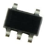
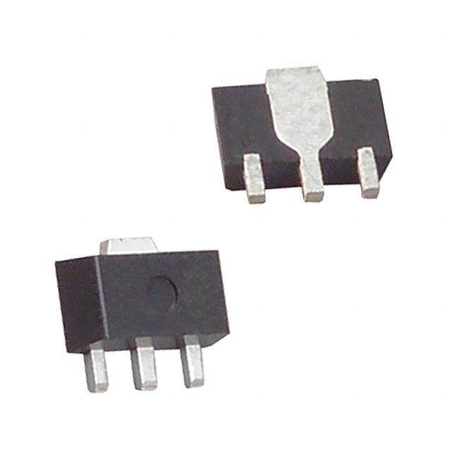
| 描述 | IC REG LDO 3V 50MA SOT23-5低压差稳压器 50mA 3V LDO |
| 产品分类 | |
| 品牌 | Texas Instruments |
| 产品手册 | |
| 产品图片 |
|
| rohs | 符合RoHS无铅 / 符合限制有害物质指令(RoHS)规范要求 |
| 产品系列 | 电源管理 IC,低压差稳压器,Texas Instruments TPS76030DBVR- |
| 数据手册 | |
| 产品型号 | TPS76030DBVR |
| 产品目录页面 | |
| 产品种类 | 低压差稳压器 |
| 供应商器件封装 | SOT-23-5 |
| 其它名称 | 296-1363-6 |
| 包装 | Digi-Reel® |
| 单位重量 | 13 mg |
| 商标 | Texas Instruments |
| 回动电压—最大值 | 180 mV |
| 安装类型 | 表面贴装 |
| 安装风格 | SMD/SMT |
| 封装 | Reel |
| 封装/外壳 | SC-74A,SOT-753 |
| 封装/箱体 | SOT-23-5 |
| 工作温度 | -40°C ~ 125°C |
| 工厂包装数量 | 3000 |
| 最大功率耗散 | 0.555 W |
| 最大工作温度 | + 125 C |
| 最大输入电压 | 16 V |
| 最小工作温度 | - 40 C |
| 最小输入电压 | + 3.2 V |
| 标准包装 | 1 |
| 电压-跌落(典型值) | 0.12V @ 50mA |
| 电压-输入 | 3.2 V ~ 16 V |
| 电压-输出 | 3V |
| 电压调节准确度 | 2 % |
| 电流-输出 | 50mA |
| 电流-限制(最小值) | 100mA |
| 稳压器拓扑 | 正,固定式 |
| 稳压器数 | 1 |
| 系列 | TPS76030 |
| 线路调整率 | 10 mV |
| 输入偏压电流—最大 | 0.09 mA |
| 输出电压 | 3 V |
| 输出电流 | 50 mA |
| 输出端数量 | 1 Output |
| 输出类型 | Fixed |
| 配用 | /product-detail/zh/TPS76XXXEVM-125/296-11042-ND/381857/product-detail/zh/DEM-SOT23LDO/296-20843-ND/1216448 |


- 商务部:美国ITC正式对集成电路等产品启动337调查
- 曝三星4nm工艺存在良率问题 高通将骁龙8 Gen1或转产台积电
- 太阳诱电将投资9.5亿元在常州建新厂生产MLCC 预计2023年完工
- 英特尔发布欧洲新工厂建设计划 深化IDM 2.0 战略
- 台积电先进制程称霸业界 有大客户加持明年业绩稳了
- 达到5530亿美元!SIA预计今年全球半导体销售额将创下新高
- 英特尔拟将自动驾驶子公司Mobileye上市 估值或超500亿美元
- 三星加码芯片和SET,合并消费电子和移动部门,撤换高东真等 CEO
- 三星电子宣布重大人事变动 还合并消费电子和移动部门
- 海关总署:前11个月进口集成电路产品价值2.52万亿元 增长14.8%


PDF Datasheet 数据手册内容提取
TPS76030, TPS76032, TPS76033, TPS76038, TPS76050 LOW-POWER 50-mA LOW-DROPOUT LINEAR REGULATORS SLVS144D – JULY 1998 – REVISED MAY 2001 (cid:0) 50-mA Low-Dropout Regulator DBV PACKAGE (cid:0) (TOP VIEW) Fixed Output Voltage Options: 5 V, 3.8 V, 3.3 V, 3.2 V, and 3 V EN GND IN (cid:0) Dropout Typically 120 mV at 50 mA (cid:0) Thermal Protection 3 2 1 (cid:0) Less Than 1-µA Quiescent Current in 4 5 Shutdown (cid:0) –40°C to 125°C Operating Junction Temperature Range NC OUT (cid:0) NC – No internal connection 5-Pin SOT-23 Package (cid:0) ESD Protection Verified to 1.5 kV Human Body Model (HBM) per MIL-STD-883C description The TPS760xx is a 50 mA, low dropout (LDO) voltage regulator designed specifically for battery-powered applications. A proprietary BiCMOS fabrication process allows the TPS760xx to provide outstanding performance in all specifications critical to battery-powered operation. The TPS760xx is available in a space-saving SOT–23 package and operates over a junction temperature range of –40°C to 125°C. AVAILABLE OPTIONS TJ VOLTAGE PACKAGE PART NUMBER SYMBOL 3 V TPS76030DBVR PAGI 3.2 V TPS76032DBVR PAOI –40°C to 125°C 3.3 V SOT-23 TPS76033DBVR PAHI 3.8 V TPS76038DBVR PAJI 5 V TPS76050DBVR PANI NOTE: The DBV package is available taped and reeled only. functional block diagram † IN CS OUT EN Current Limit Vref + Thermal Sense GND †Current sense Please be aware that an important notice concerning availability, standard warranty, and use in critical applications of TexasInstruments semiconductor products and disclaimers thereto appears at the end of this data sheet. PRODUCTION DATA information is current as of publication date. Copyright 2001, Texas Instruments Incorporated Products conform to specifications per the terms of Texas Instruments standard warranty. Production processing does not necessarily include testing of all parameters. POST OFFICE BOX 655303 • DALLAS, TEXAS 75265 1
TPS76030, TPS76032, TPS76033, TPS76038, TPS76050 LOW-POWER 50-mA LOW-DROPOUT LINEAR REGULATORS SLVS144D – JULY 1998 – REVISED MAY 2001 Terminal Functions TERMINAL II//OO DDEESSCCRRIIPPTTIIOONN NAME NO. EN 3 I Enable input GND 2 Ground IN 1 I Input voltage NC 4 No connection OUT 5 O Regulated output voltage absolute maximum ratings over operating free-air temperature range (unless otherwise noted)† Input voltage range, VI‡. . . . . . . . . . . . . . . . . . . . . . . . . . . . . . . . . . . . . . . . . . . . . . . . . . . . . . . . . . . . . . . . . . . –0.3 V to 16 V Voltage range at EN . . . . . . . . . . . . . . . . . . . . . . . . . . . . . . . . . . . . . . . . . . . . . . . . . . . . . . . . . . . . . . . . . –0.3 V to VI + 0.3 V Peak output current . . . . . . . . . . . . . . . . . . . . . . . . . . . . . . . . . . . . . . . . . . . . . . . . . . . . . . . . . . . . . . . internally limited Continuous total dissipation . . . . . . . . . . . . . . . . . . . . . . . . . . . . . . . . . . . . . . . . . . . . See Dissipation Rating Table Operating junction temperature range, T . . . . . . . . . . . . . . . . . . . . . . . . . . . . . . . . . . . . . . . . . . . –40°C to 150°C J Storage temperature range, Tstg . . . . . . . . . . . . . . . . . . . . . . . . . . . . . . . . . . . . . . . . . . . . . . . . . . . . . . . . . –65°C to 150°C ESD rating, HBM . . . . . . . . . . . . . . . . . . . . . . . . . . . . . . . . . . . . . . . . . . . . . . . . . . . . . . . . . . . . . . . . . . . . . . . . . 1.5 kV †Stresses beyond those listed under “absolute maximum ratings” may cause permanent damage to the device. These are stress ratings only, and functional operation of the device at these or any other conditions beyond those indicated under “recommended operating conditions” is not implied. Exposure to absolute-maximum-rated conditions for extended periods may affect device reliability. ‡All voltages are with respect to device GND pin. DISSIPATION RATING TABLE DERATING FACTOR TA ≤ 25°C TA = 70°C TA = 85°C BOARD PACKAGE RθJC RθJA ABOVE TA = 25°C POWER RATING POWER RATING POWER RATING Low K§ DBV 65.8 °C/W 259 °C/W 3.9 mW/°C 386 mW 212 mW 154 mW High K¶ DBV 65.8 °C/W 180 °C/W 5.6 mW/°C 555 mW 305 mW 222 mW §The JEDEC Low K (1s) board design used to derive this data was a 3 inch x 3 inch, two layer board with 2 ounce copper traces on top of the board. ¶The JEDEC High K (2s2p) board design used to derive this data was a 3 inch x 3 inch, multilayer board with 1 ounce internal power and ground planes and 2 ounce copper traces on top and bottom of the board. recommended operating conditions MIN NOM MAX UNIT TPS76030 3.2 16 TPS76032 3.4 16 Input voltage, VI TPS76033 3.5 16 V TPS76038 4 16 TPS76050 5.2 16 Continuous output current, IO 0 50 mA Operating junction temperature, TJ –40 125 °C 2 POST OFFICE BOX 655303 • DALLAS, TEXAS 75265
TPS76030, TPS76032, TPS76033, TPS76038, TPS76050 LOW-POWER 50-mA LOW-DROPOUT LINEAR REGULATORS SLVS144D – JULY 1998 – REVISED MAY 2001 electrical characteristics over recommended operating free-air temperature range, V = V + 1 V, I = 1 mA, EN = V, C = 2.2 µF (unless otherwise noted) I O(nom) O I o PARAMETER TEST CONDITIONS MIN TYP MAX UNIT TJ = 25°C 2.96 3 3.04 TPS76030 TJ = 25°C, 1 mA < IO < 50 mA 2.92 3.04 V 1 mA < IO < 50 mA 2.91 3.07 TJ = 25°C 3.16 3.2 3.24 TPS76032 TJ = 25°C, 1 mA < IO < 50 mA 3.13 3.24 V 1 mA < IO < 50 mA 3.1 3.3 TJ = 25°C 3.26 3.3 3.34 VO Output voltage TPS76033 TJ = 25°C, 1 mA < IO < 50 mA 3.23 3.34 V 1 mA < IO < 50 mA 3.2 3.4 TJ = 25°C 3.76 3.8 3.84 TPS76038 TJ = 25°C, 1 mA < IO < 50 mA 3.73 3.84 V 1 mA < IO < 50 mA 3.7 3.9 TJ = 25°C 4.95 5 5.05 TPS76050 TJ = 25°C, 1 mA < IO < 50 mA 4.91 5.05 V 1 mA < IO < 50 mA 4.89 5.1 II(standby) Standby current EN = 0 V 1 µA IO = 0 mA, TJ = 25°C 90 115 IO = 0 mA 130 IO = 1 mA, TJ = 25°C 100 130 IO = 1 mA 170 QQuuiieesscceenntt ccuurrrreenntt ((GGNNDD ccuurrrreenntt)) µµAA IO = 10 mA, TJ = 25°C 190 215 IO = 10 mA 260 IO = 50 mA, TJ = 25°C 850 1100 IO = 50 mA 1200 TPS76030 4 V < VI < 16, IO = 1 mA 3 10 TPS76032 4.2 V < VI < 16, IO = 1 mA 3 10 Input regulation TPS76033 4.3 V < VI < 16, IO = 1 mA 3 10 mV TPS76038 4.8 V < VI < 16, IO = 1 mA 3 10 TPS76050 6 V < VI < 16, IO = 1 mA 3 10 Vn Output noise voltage BW = 300 Hz to 50 kHz, Co = 10 µF, TJ = 25°C 190 µVrms Ripple rejection f = 1 kHz, Co = 10 µF, TJ = 25°C 63 dB IO = 0 mA TJ = 25°C 1 3 IO = 0 mA 5 IO = 1 mA, TJ = 25°C 7 10 IO = 1 mA 15 DDrrooppoouutt vvoollttaaggee mmVV IO = 10 mA, TJ = 25°C 40 60 IO = 10 mA 90 IO = 50 mA TJ = 25°C 120 150 IO = 50 mA 180 Peak output current/current limit 100 125 135 mA High level enable input 2 V Low level enable input 0.8 V EN = 0 V –1 0 1 µA IIII IInnppuutt ccuurrrreenntt ((EENN)) EN = VI 2.5 5 µA POST OFFICE BOX 655303 • DALLAS, TEXAS 75265 3
TPS76030, TPS76032, TPS76033, TPS76038, TPS76050 LOW-POWER 50-mA LOW-DROPOUT LINEAR REGULATORS SLVS144D – JULY 1998 – REVISED MAY 2001 Table of Graphs FIGURE vs Output current 1, 2, 3 VVOO OOuuttppuutt vvoollttaaggee vs Free-air temperature 4, 5, 6 Ground current vs Free-air temperature 7, 8, 9 Output noise vs Frequency 10 Zo Output impedance vs Frequency 11 VDO Dropout voltage vs Free-air temperature 12 Line transient response 13, 15 Load transient response 14, 16 4 POST OFFICE BOX 655303 • DALLAS, TEXAS 75265
TPS76030, TPS76032, TPS76033, TPS76038, TPS76050 LOW-POWER 50-mA LOW-DROPOUT LINEAR REGULATORS SLVS144D – JULY 1998 – REVISED MAY 2001 TYPICAL CHARACTERISTICS TPS76030 TPS76033 OUTPUT VOLTAGE OUTPUT VOLTAGE vs vs OUTPUT CURRENT OUTPUT CURRENT 3.005 3.305 VI = 4 V VI = 4.3 V TA = 25°C 3.3 TA = 25°C 3 3.295 V V – 2.995 – e e g g a a 3.29 olt olt V 2.99 V put put 3.285 ut ut O O – O 2.985 – O 3.28 V V 2.98 3.275 2.975 3.27 0 10 20 30 40 50 60 0 10 20 30 40 50 60 IO – Output Current – mA IO – Output Current – mA Figure 1 Figure 2 TPS76050 TPS76030 OUTPUT VOLTAGE OUTPUT VOLTAGE vs vs OUTPUT CURRENT FREE-AIR TEMPERATURE 5.02 3.15 VI = 6 V VI = 4 V TA = 25°C 5.01 3.1 V– Output Voltage – VO 44..99589 V– Output Voltage – VO 23..90355 IIOO == 15 0m mAA 4.97 2.9 4.96 2.85 0 10 20 30 40 50 60 –55 –35 –15 5 25 45 65 85 105 125 IO – Output Current – mA TA – Free-Air Temperature – °C Figure 3 Figure 4 POST OFFICE BOX 655303 • DALLAS, TEXAS 75265 5
TPS76030, TPS76032, TPS76033, TPS76038, TPS76050 LOW-POWER 50-mA LOW-DROPOUT LINEAR REGULATORS SLVS144D – JULY 1998 – REVISED MAY 2001 TYPICAL CHARACTERISTICS TPS76033 TPS76050 OUTPUT VOLTAGE OUTPUT VOLTAGE vs vs FREE-AIR TEMPERATURE FREE-AIR TEMPERATURE 3.35 5.1 VI = 4.3 V VI = 6 V IO = 1 mA 5.08 5.06 3.3 V V 5.04 ge – IO = 50 mA ge – 5.02 IO = 1 mA a a olt olt V 3.25 V 5 ut ut p p ut ut 4.98 IO = 50 mA O O – – O O 4.96 V 3.2 V 4.94 4.92 3.15 4.9 –55 –35 –15 5 25 45 65 85 105 125 –55 –35 –15 5 25 45 65 85 105 125 TA – Free-Air Temperature – °C TA – Free-Air Temperature – °C Figure 5 Figure 6 TPS76030 TPS76033 GROUND CURRENT GROUND CURRENT vs vs FREE-AIR TEMPERATURE FREE-AIR TEMPERATURE 10000 10000 VI = 4 V VI = 4.3 V A 1000 IO = 50 mA A 1000 IO = 50 mA µ µ – – nt nt e e Curr IO = 10 mA Curr IO = 10 mA d d n n ou 100 IO = 1 mA ou 100 IO = 1 mA Gr Gr IO = 0 mA IO = 0 mA 10 10 –55 –35 –15 5 25 45 65 85 105 125 –55 –35 –15 5 25 45 65 85 105 125 TA – Free-Air Temperature – °C TA – Free-Air Temperature – °C Figure 7 Figure 8 6 POST OFFICE BOX 655303 • DALLAS, TEXAS 75265
TPS76030, TPS76032, TPS76033, TPS76038, TPS76050 LOW-POWER 50-mA LOW-DROPOUT LINEAR REGULATORS SLVS144D – JULY 1998 – REVISED MAY 2001 TYPICAL CHARACTERISTICS TPS76050 OUTPUT NOISE GROUND CURRENT vs vs FREQUENCY FREE-AIR TEMPERATURE 10µV(cid:0)Hz 10000 VI = 6 V CL = 2.2 µF CL = 2.2 µF IO = 50 mA IO = 1 mA 10µV(cid:0)Hz IO = 50 mA A 1000 e µ s – oi ent ut N 1µV(cid:0)Hz d Curr IO = 10 mA Outp CL = 10 µF n u IO = 50 mA o 100 IO = 1 mA r G 100nV(cid:0)Hz IO = 0 mA CL = 10 µF IO = 1 mA 10nV(cid:0)Hz 10 250 1k 10k 100k –55 –35 –15 5 25 45 65 85 105 125 f – Frequency – Hz TA – Free-Air Temperature – °C Figure 9 Figure 10 TPS76030 OUTPUT IMPEDANCE DROPOUT VOLTAGE vs vs FREQUENCY FREE-AIR TEMPERATURE 10 150 CL = 2.2 µF: VI = EN = 2.9 V IO = 1 mA 50 mA IO = 10 mA 125 IO = 50 mA Ω V m nce – CL = 10 µF: ge – 100 peda IIOO == 110 m mAA Volta ut Im 1 pout 75 utp Dro 10 mA – O CL = 10 µF – O 50 Zo IO = 50 mA VD 25 0 mA 1 mA 0.1 0 0.01 0.1 1 10 100 1000 –55 –35 –15 5 25 45 65 85 105 125 f – Frequency – kHz TA – Free-Air Temperature – °C Figure 11 Figure 12 POST OFFICE BOX 655303 • DALLAS, TEXAS 75265 7
TPS76030, TPS76032, TPS76033, TPS76038, TPS76050 LOW-POWER 50-mA LOW-DROPOUT LINEAR REGULATORS SLVS144D – JULY 1998 – REVISED MAY 2001 TYPICAL CHARACTERISTICS TPS76033 TPS76033 LINE TRANSIENT RESPONSE LOAD TRANSIENT RESPONSE 40 100 V CO = 2.2 µF V nm ge ine – m 20 nge ige – 50 ng aa – ChaOut Volta –200 V– ChOput Volt –500 ∆Vutp ∆ Out O –30 –100 A m – – V 6 ent 60 e rr ag 5 Cu 40 olt ut V p ut 4 ut 20 p O V– InI 30 C2O0 = 24.20 µF60 80 100 120 140 160 180 200 I – O 00 20 40 60 80 100 120 140 160 180 200 t – Time – µs t – Time – µs Figure 13 Figure 14 TPS76050 TPS76050 LINE TRANSIENT RESPONSE LOAD TRANSIENT RESPONSE 60 150 V V nm ge ine – m 40 nge ige – 100 ng aa ∆V– ChaOOutput Volta 200 ∆V– ChOOutput Volt 500 CO = 2.2 µF –20 A –50 m V – age – 8 rrent 60 ut Volt 7 put Cu 40 V– InpI 65 CO = 2.2 µF I – OutO 200 0 50 100 150 200 250 300 350 400 450 500 0 20 40 60 80 100 120 140 160 180 200 t – Time – µs t – Time – µs Figure 15 Figure 16 8 POST OFFICE BOX 655303 • DALLAS, TEXAS 75265
TPS76030, TPS76032, TPS76033, TPS76038, TPS76050 LOW-POWER 50-mA LOW-DROPOUT LINEAR REGULATORS SLVS144D – JULY 1998 – REVISED MAY 2001 APPLICATION INFORMATION 1 5 IN OUT CI = 1 µF Co = 2.2 µF TPS760xx 3 EN 2 GND Figure 17. TPS760xx Typical Application over current protection The over current protection circuit forces the TPS760xx into a constant current output mode when the load is excessive or the output is shorted to ground. Normal operation resumes when the fault condition is removed. An overload or short circuit may also activate the over temperature protection if the fault condition persists. over temperature protection The thermal protection system shuts the TPS760xx down when the junction temperature exceeds 160°C. The device recovers and operates normally when the temperature drops below 155°C. input capacitor A 0.047 µF or larger ceramic decoupling capacitor with short leads connected between IN and GND is recommended. The decoupling capacitor may be omitted if there is a 1 µF or larger electrolytic capacitor connected between IN and GND and located reasonably close to the TPS760xx. However, the small ceramic device is desirable even when the larger capacitor is present, if there is a lot of high frequency noise present in the system. output capacitor Like all low dropout regulators, the TPS760xx requires an output capacitor connected between OUT and GND to stabilize the internal control loop. The minimum recommended capacitance value is 2.2 µF and the ESR (equivalent series resistance) must be between 0.1 Ω and 20 Ω. Capacitor values of 2.5-µF or larger are acceptable, provided the ESR is less than 20 Ω. Solid tantalum electrolytic, aluminum electrolytic, and multilayer ceramic capacitors are all suitable, provided they meet the requirements described above. Most of the commercially available 2.2-µF surface-mount solid-tantalum capacitors, including devices from Sprague, Kemet, and Nichicon, meet the ESR requirements stated above. Multilayer ceramic capacitors should have minimum values of 2.5 µF over the full operating temperature range of the equipment. enable (EN) µ A logic zero on the enable input shuts the TPS760xx off and reduces the supply current to less than 1 A. Pulling the enable input high causes normal operation to resume. If the enable feature is not used, EN should be connected to IN to keep the regulator on all of the time. The EN input must not be left floating. reverse current path The power transistor used in the TPS760xx has an inherent diode connected between IN and OUT as shown in the functional block diagram. This diode conducts current from the OUT terminal to the IN terminal whenever IN is lower than OUT by a diode drop. This condition does not damage the TPS760xx, provided the current is limited to 100 mA. POST OFFICE BOX 655303 • DALLAS, TEXAS 75265 9
PACKAGE OPTION ADDENDUM www.ti.com 6-Feb-2020 PACKAGING INFORMATION Orderable Device Status Package Type Package Pins Package Eco Plan Lead/Ball Finish MSL Peak Temp Op Temp (°C) Device Marking Samples (1) Drawing Qty (2) (6) (3) (4/5) TPS76030DBVR ACTIVE SOT-23 DBV 5 3000 Green (RoHS NIPDAU Level-1-260C-UNLIM -40 to 125 PAGI & no Sb/Br) TPS76030DBVT ACTIVE SOT-23 DBV 5 250 Green (RoHS NIPDAU Level-1-260C-UNLIM -40 to 125 PAGI & no Sb/Br) TPS76032DBVR ACTIVE SOT-23 DBV 5 3000 Green (RoHS NIPDAU Level-1-260C-UNLIM -40 to 125 PAOI & no Sb/Br) TPS76033DBVR ACTIVE SOT-23 DBV 5 3000 Green (RoHS NIPDAU Level-1-260C-UNLIM -40 to 125 PAHI & no Sb/Br) TPS76033DBVT ACTIVE SOT-23 DBV 5 250 Green (RoHS NIPDAU Level-1-260C-UNLIM -40 to 125 PAHI & no Sb/Br) TPS76038DBVR ACTIVE SOT-23 DBV 5 3000 Green (RoHS NIPDAU Level-1-260C-UNLIM -40 to 125 PAJI & no Sb/Br) TPS76038DBVT ACTIVE SOT-23 DBV 5 250 Green (RoHS NIPDAU Level-1-260C-UNLIM -40 to 125 PAJI & no Sb/Br) TPS76050DBVR ACTIVE SOT-23 DBV 5 3000 Green (RoHS NIPDAU Level-1-260C-UNLIM -40 to 125 PANI & no Sb/Br) TPS76050DBVRG4 ACTIVE SOT-23 DBV 5 3000 Green (RoHS NIPDAU Level-1-260C-UNLIM -40 to 125 PANI & no Sb/Br) TPS76050DBVT ACTIVE SOT-23 DBV 5 250 Green (RoHS NIPDAU Level-1-260C-UNLIM -40 to 125 PANI & no Sb/Br) (1) The marketing status values are defined as follows: ACTIVE: Product device recommended for new designs. LIFEBUY: TI has announced that the device will be discontinued, and a lifetime-buy period is in effect. NRND: Not recommended for new designs. Device is in production to support existing customers, but TI does not recommend using this part in a new design. PREVIEW: Device has been announced but is not in production. Samples may or may not be available. OBSOLETE: TI has discontinued the production of the device. (2) RoHS: TI defines "RoHS" to mean semiconductor products that are compliant with the current EU RoHS requirements for all 10 RoHS substances, including the requirement that RoHS substance do not exceed 0.1% by weight in homogeneous materials. Where designed to be soldered at high temperatures, "RoHS" products are suitable for use in specified lead-free processes. TI may reference these types of products as "Pb-Free". RoHS Exempt: TI defines "RoHS Exempt" to mean products that contain lead but are compliant with EU RoHS pursuant to a specific EU RoHS exemption. Green: TI defines "Green" to mean the content of Chlorine (Cl) and Bromine (Br) based flame retardants meet JS709B low halogen requirements of <=1000ppm threshold. Antimony trioxide based flame retardants must also meet the <=1000ppm threshold requirement. (3) MSL, Peak Temp. - The Moisture Sensitivity Level rating according to the JEDEC industry standard classifications, and peak solder temperature. Addendum-Page 1
PACKAGE OPTION ADDENDUM www.ti.com 6-Feb-2020 (4) There may be additional marking, which relates to the logo, the lot trace code information, or the environmental category on the device. (5) Multiple Device Markings will be inside parentheses. Only one Device Marking contained in parentheses and separated by a "~" will appear on a device. If a line is indented then it is a continuation of the previous line and the two combined represent the entire Device Marking for that device. (6) Lead/Ball Finish - Orderable Devices may have multiple material finish options. Finish options are separated by a vertical ruled line. Lead/Ball Finish values may wrap to two lines if the finish value exceeds the maximum column width. Important Information and Disclaimer:The information provided on this page represents TI's knowledge and belief as of the date that it is provided. TI bases its knowledge and belief on information provided by third parties, and makes no representation or warranty as to the accuracy of such information. Efforts are underway to better integrate information from third parties. TI has taken and continues to take reasonable steps to provide representative and accurate information but may not have conducted destructive testing or chemical analysis on incoming materials and chemicals. TI and TI suppliers consider certain information to be proprietary, and thus CAS numbers and other limited information may not be available for release. In no event shall TI's liability arising out of such information exceed the total purchase price of the TI part(s) at issue in this document sold by TI to Customer on an annual basis. Addendum-Page 2
PACKAGE MATERIALS INFORMATION www.ti.com 24-Apr-2020 TAPE AND REEL INFORMATION *Alldimensionsarenominal Device Package Package Pins SPQ Reel Reel A0 B0 K0 P1 W Pin1 Type Drawing Diameter Width (mm) (mm) (mm) (mm) (mm) Quadrant (mm) W1(mm) TPS76030DBVR SOT-23 DBV 5 3000 180.0 9.0 3.15 3.2 1.4 4.0 8.0 Q3 TPS76030DBVT SOT-23 DBV 5 250 180.0 9.0 3.15 3.2 1.4 4.0 8.0 Q3 TPS76032DBVR SOT-23 DBV 5 3000 180.0 9.0 3.15 3.2 1.4 4.0 8.0 Q3 TPS76033DBVR SOT-23 DBV 5 3000 178.0 9.0 3.23 3.17 1.37 4.0 8.0 Q3 TPS76033DBVT SOT-23 DBV 5 250 178.0 9.0 3.23 3.17 1.37 4.0 8.0 Q3 TPS76038DBVR SOT-23 DBV 5 3000 180.0 9.0 3.15 3.2 1.4 4.0 8.0 Q3 TPS76038DBVT SOT-23 DBV 5 250 180.0 9.0 3.15 3.2 1.4 4.0 8.0 Q3 TPS76050DBVR SOT-23 DBV 5 3000 178.0 9.0 3.23 3.17 1.37 4.0 8.0 Q3 TPS76050DBVT SOT-23 DBV 5 250 178.0 9.0 3.23 3.17 1.37 4.0 8.0 Q3 PackMaterials-Page1
PACKAGE MATERIALS INFORMATION www.ti.com 24-Apr-2020 *Alldimensionsarenominal Device PackageType PackageDrawing Pins SPQ Length(mm) Width(mm) Height(mm) TPS76030DBVR SOT-23 DBV 5 3000 182.0 182.0 20.0 TPS76030DBVT SOT-23 DBV 5 250 182.0 182.0 20.0 TPS76032DBVR SOT-23 DBV 5 3000 182.0 182.0 20.0 TPS76033DBVR SOT-23 DBV 5 3000 180.0 180.0 18.0 TPS76033DBVT SOT-23 DBV 5 250 180.0 180.0 18.0 TPS76038DBVR SOT-23 DBV 5 3000 182.0 182.0 20.0 TPS76038DBVT SOT-23 DBV 5 250 182.0 182.0 20.0 TPS76050DBVR SOT-23 DBV 5 3000 180.0 180.0 18.0 TPS76050DBVT SOT-23 DBV 5 250 180.0 180.0 18.0 PackMaterials-Page2
PACKAGE OUTLINE DBV0005A SOT-23 - 1.45 mm max height SCALE 4.000 SMALL OUTLINE TRANSISTOR C 3.0 2.6 0.1 C 1.75 1.45 1.45 B A 0.90 PIN 1 INDEX AREA 1 5 2X 0.95 3.05 2.75 1.9 1.9 2 4 3 0.5 5X 0.3 0.15 0.2 C A B (1.1) TYP 0.00 0.25 GAGE PLANE 0.22 TYP 0.08 8 TYP 0.6 0 0.3 TYP SEATING PLANE 4214839/E 09/2019 NOTES: 1. All linear dimensions are in millimeters. Any dimensions in parenthesis are for reference only. Dimensioning and tolerancing per ASME Y14.5M. 2. This drawing is subject to change without notice. 3. Refernce JEDEC MO-178. 4. Body dimensions do not include mold flash, protrusions, or gate burrs. Mold flash, protrusions, or gate burrs shall not exceed 0.15 mm per side. www.ti.com
EXAMPLE BOARD LAYOUT DBV0005A SOT-23 - 1.45 mm max height SMALL OUTLINE TRANSISTOR PKG 5X (1.1) 1 5 5X (0.6) SYMM (1.9) 2 2X (0.95) 3 4 (R0.05) TYP (2.6) LAND PATTERN EXAMPLE EXPOSED METAL SHOWN SCALE:15X SOLDER MASK SOLDER MASK METAL UNDER METAL OPENING OPENING SOLDER MASK EXPOSED METAL EXPOSED METAL 0.07 MAX 0.07 MIN ARROUND ARROUND NON SOLDER MASK SOLDER MASK DEFINED DEFINED (PREFERRED) SOLDER MASK DETAILS 4214839/E 09/2019 NOTES: (continued) 5. Publication IPC-7351 may have alternate designs. 6. Solder mask tolerances between and around signal pads can vary based on board fabrication site. www.ti.com
EXAMPLE STENCIL DESIGN DBV0005A SOT-23 - 1.45 mm max height SMALL OUTLINE TRANSISTOR PKG 5X (1.1) 1 5 5X (0.6) SYMM 2 (1.9) 2X(0.95) 3 4 (R0.05) TYP (2.6) SOLDER PASTE EXAMPLE BASED ON 0.125 mm THICK STENCIL SCALE:15X 4214839/E 09/2019 NOTES: (continued) 7. Laser cutting apertures with trapezoidal walls and rounded corners may offer better paste release. IPC-7525 may have alternate design recommendations. 8. Board assembly site may have different recommendations for stencil design. www.ti.com
IMPORTANTNOTICEANDDISCLAIMER TI PROVIDES TECHNICAL AND RELIABILITY DATA (INCLUDING DATASHEETS), DESIGN RESOURCES (INCLUDING REFERENCE DESIGNS), APPLICATION OR OTHER DESIGN ADVICE, WEB TOOLS, SAFETY INFORMATION, AND OTHER RESOURCES “AS IS” AND WITH ALL FAULTS, AND DISCLAIMS ALL WARRANTIES, EXPRESS AND IMPLIED, INCLUDING WITHOUT LIMITATION ANY IMPLIED WARRANTIES OF MERCHANTABILITY, FITNESS FOR A PARTICULAR PURPOSE OR NON-INFRINGEMENT OF THIRD PARTY INTELLECTUAL PROPERTY RIGHTS. These resources are intended for skilled developers designing with TI products. You are solely responsible for (1) selecting the appropriate TI products for your application, (2) designing, validating and testing your application, and (3) ensuring your application meets applicable standards, and any other safety, security, or other requirements. These resources are subject to change without notice. TI grants you permission to use these resources only for development of an application that uses the TI products described in the resource. Other reproduction and display of these resources is prohibited. No license is granted to any other TI intellectual property right or to any third party intellectual property right. TI disclaims responsibility for, and you will fully indemnify TI and its representatives against, any claims, damages, costs, losses, and liabilities arising out of your use of these resources. TI’s products are provided subject to TI’s Terms of Sale (www.ti.com/legal/termsofsale.html) or other applicable terms available either on ti.com or provided in conjunction with such TI products. TI’s provision of these resources does not expand or otherwise alter TI’s applicable warranties or warranty disclaimers for TI products. Mailing Address: Texas Instruments, Post Office Box 655303, Dallas, Texas 75265 Copyright © 2020, Texas Instruments Incorporated