ICGOO在线商城 > 射频/IF 和 RFID > RF 接收器 > MICRF211AYQS
 Datasheet下载
- 型号: MICRF211AYQS
- 制造商: Micrel
- 库位|库存: xxxx|xxxx
- 要求:
| 数量阶梯 | 香港交货 | 国内含税 |
| +xxxx | $xxxx | ¥xxxx |
查看当月历史价格
查看今年历史价格
MICRF211AYQS产品简介:
ICGOO电子元器件商城为您提供MICRF211AYQS由Micrel设计生产,在icgoo商城现货销售,并且可以通过原厂、代理商等渠道进行代购。 MICRF211AYQS价格参考¥20.44-¥21.29。MicrelMICRF211AYQS封装/规格:RF 接收器, - RF Receiver ASK, OOK 380MHz ~ 450MHz -110dBm 10 kbps PCB, Surface Mount 16-QSOP。您可以下载MICRF211AYQS参考资料、Datasheet数据手册功能说明书,资料中有MICRF211AYQS 详细功能的应用电路图电压和使用方法及教程。
Microchip Technology的RF接收器型号MICRF211AYQS是一款高性能、低功耗的射频接收器,广泛应用于各种无线通信场景。该器件主要工作在315 MHz和433.92 MHz频段,适用于短距离无线数据传输。以下是其主要应用场景:

1. 智能家居:MICRF211AYQS可用于智能家居设备中的无线控制模块,如智能门锁、智能插座、智能照明等。它能够接收来自遥控器或智能手机的指令,实现远程控制和自动化操作。

2. 安防系统:在家庭或商业安防系统中,该接收器可以用于接收门窗传感器、运动探测器等设备发送的信号,及时将警报信息传递给中央控制器或用户终端,增强安全防护能力。

3. 工业自动化:在工业环境中,MICRF211AYQS可以集成到各种传感器和执行器中,实现无线数据采集与控制。例如,它可以用于监控温度、湿度、压力等参数,并将数据传输到中央控制系统进行分析和处理。

4. 消费电子:该接收器还可应用于消费电子产品,如无线鼠标、键盘、游戏手柄等外设,提供稳定可靠的无线连接,减少线缆束缚,提升用户体验。

5. 远程控制:MICRF211AYQS适合用于各种遥控设备,如车库门开启器、电动窗帘控制器、玩具遥控车等。它能够接收用户通过遥控器发出的指令,实现对目标设备的精确控制。

6. 物联网(IoT):随着物联网技术的发展,MICRF211AYQS可以作为节点设备的一部分,与其他传感器和网关配合使用,构建低成本、低功耗的无线传感网络,广泛应用于环境监测、资产管理等领域。

总之,MICRF211AYQS凭借其优异的性能和灵活性,成为众多无线通信应用的理想选择。
| 参数 | 数值 |
| 产品目录 | |
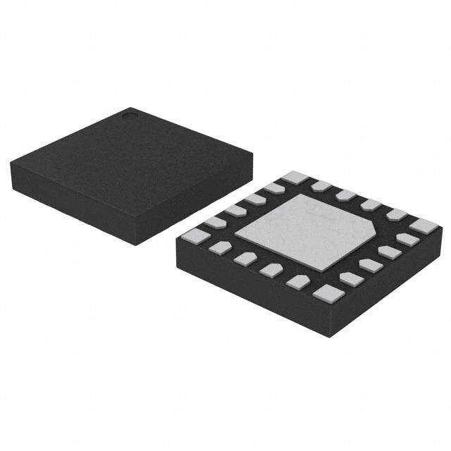
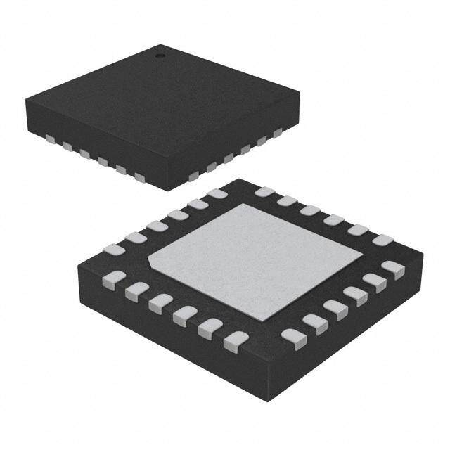
| 描述 | IC RX 3V 380-450 MHZ 16-QSOP射频接收器 380MHz to 450MHz, 3.0V to 3.6V, 6mA, 10kbps, ASK Receiver with RSSI and Shutdown in 16-Lead QSOP (Lead-Free) |
| 产品分类 | |
| 品牌 | Micrel Inc |
| 产品手册 | |
| 产品图片 |
|
| rohs | 符合RoHS无铅 / 符合限制有害物质指令(RoHS)规范要求 |
| 产品系列 | RF集成电路,射频接收器,Micrel MICRF211AYQS- |
| 数据手册 | |
| 产品型号 | MICRF211AYQS |
| 产品目录页面 | |
| 产品种类 | 射频接收器 |
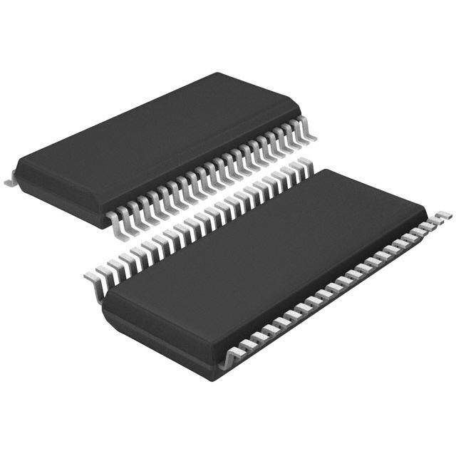
| 供应商器件封装 | 16-QSOP |
| 其它名称 | 576-1964-5 |
| 包装 | 管件 |
| 商标 | Micrel |
| 天线连接器 | PCB,表面贴装 |
| 存储容量 | - |
| 安装风格 | SMD/SMT |
| 封装 | Tube |
| 封装/外壳 | 16-SSOP(0.154",3.90mm 宽) |
| 封装/箱体 | QSOP-16 |
| 工作温度 | -40°C ~ 105°C |
| 工作电源电压 | 3 V to 3.6 V |
| 工作频率 | 380 MHz to 450 Mhz |
| 工厂包装数量 | 98 |
| 带宽 | 330 kHz |
| 应用 | ISM,车库门开启器,RKE |
| 数据接口 | PCB,表面贴装 |
| 数据速率(最大值) | 10 kbps |
| 最大工作温度 | + 105 C |
| 最小工作温度 | - 40 C |
| 标准包装 | 98 |
| 灵敏度 | -110dBm |
| 特性 | 无需 IF 滤波器 |
| 电压-电源 | 3 V ~ 3.6 V |
| 电流-接收 | 6mA |
| 电源电压-最大 | 3.6 V |
| 电源电压-最小 | 3 V |
| 电源电流 | 6 mA |
| 类型 | RF Receiver |
| 系列 | MICRF211 |
| 调制或协议 | ASK,OOK |
| 配用 | /product-detail/zh/MICRF211-433%20EV/576-4573-ND/4800156/product-detail/zh/MICRF211-315%20EV/576-4572-ND/4800155/product-detail/zh/ABM7-9.81563MHZ-10-R50-J4Q-T/535-10154-6-ND/2184281/product-detail/zh/ABM7-13.52127MHZ-10-R50-J4Q-T/535-10153-6-ND/2184280/product-detail/zh/ABLS-13.0625MHZ-10-K4Q-T/535-10149-6-ND/2184276/product-detail/zh/ABLS-13.52127MHZ-10-J-4Q-T/535-10148-6-ND/2184275/product-detail/zh/ABM7-9.81563MHZ-10-R50-J4Q-T/535-10154-1-ND/2184189/product-detail/zh/ABM7-13.52127MHZ-10-R50-J4Q-T/535-10153-1-ND/2184188/product-detail/zh/ABLS-13.0625MHZ-10-K4Q-T/535-10149-1-ND/2184184/product-detail/zh/ABLS-13.52127MHZ-10-J-4Q-T/535-10148-1-ND/2184183/product-detail/zh/ABM7-9.81563MHZ-10-R50-J4Q-T/535-10154-2-ND/2184097/product-detail/zh/ABM7-13.52127MHZ-10-R50-J4Q-T/535-10153-2-ND/2184096/product-detail/zh/ABLS-13.02519MHZ-10-K4Q-T/535-10150-2-ND/2184093/product-detail/zh/ABLS-13.0625MHZ-10-K4Q-T/535-10149-2-ND/2184092/product-detail/zh/ABLS-13.52127MHZ-10-J-4Q-T/535-10148-2-ND/2184091/product-detail/zh/ABLS-14.822520MHZ-10-J4Y-T/535-9709-6-ND/1856920/product-detail/zh/ABLS-14.463660MHZ-10-J4Y-T/535-9708-6-ND/1856919/product-detail/zh/ABLS-14.299830MHZ-10-J4Y-T/535-9707-6-ND/1856918/product-detail/zh/ABLS-14.276430MHZ-10-J4Y-T/535-9706-6-ND/1856917/product-detail/zh/ABLS-14.089190MHZ-10-J4Y-T/535-9705-6-ND/1856916/product-detail/zh/ABLS-13.262250MHZ-10-J4Y-T/535-9703-6-ND/1856914/product-detail/zh/ABLS-14.822520MHZ-10-J4Y-T/535-9709-1-ND/1856913/product-detail/zh/ABLS-14.463660MHZ-10-J4Y-T/535-9708-1-ND/1856912/product-detail/zh/ABLS-14.299830MHZ-10-J4Y-T/535-9707-1-ND/1856911/product-detail/zh/ABLS-14.276430MHZ-10-J4Y-T/535-9706-1-ND/1856910/product-detail/zh/ABLS-14.089190MHZ-10-J4Y-T/535-9705-1-ND/1856909/product-detail/zh/ABLS-13.262250MHZ-10-J4Y-T/535-9703-1-ND/1856907/product-detail/zh/ABLS-14.822520MHZ-10-J4Y-T/535-9709-2-ND/1856906/product-detail/zh/ABLS-14.463660MHZ-10-J4Y-T/535-9708-2-ND/1856905/product-detail/zh/ABLS-14.299830MHZ-10-J4Y-T/535-9707-2-ND/1856904/product-detail/zh/ABLS-14.276430MHZ-10-J4Y-T/535-9706-2-ND/1856903/product-detail/zh/ABLS-14.089190MHZ-10-J4Y-T/535-9705-2-ND/1856902/product-detail/zh/ABLS-13.262250MHZ-10-J4Y-T/535-9703-2-ND/1856900 |
| 频率 | 380MHz ~ 450MHz |


- 商务部:美国ITC正式对集成电路等产品启动337调查
- 曝三星4nm工艺存在良率问题 高通将骁龙8 Gen1或转产台积电
- 太阳诱电将投资9.5亿元在常州建新厂生产MLCC 预计2023年完工
- 英特尔发布欧洲新工厂建设计划 深化IDM 2.0 战略
- 台积电先进制程称霸业界 有大客户加持明年业绩稳了
- 达到5530亿美元!SIA预计今年全球半导体销售额将创下新高
- 英特尔拟将自动驾驶子公司Mobileye上市 估值或超500亿美元
- 三星加码芯片和SET,合并消费电子和移动部门,撤换高东真等 CEO
- 三星电子宣布重大人事变动 还合并消费电子和移动部门
- 海关总署:前11个月进口集成电路产品价值2.52万亿元 增长14.8%

PDF Datasheet 数据手册内容提取
MICRF211 ® 3V, QwikRadio 433.92 MHz Receiver General Description Features The MICRF211 is a general purpose, 3V QwikRadio • –110dBm sensitivity, 1kbps and BER 10-2 Receiver that operates at 433.92MHz with typical • Image rejection mixer sensitivity of –110dBm. • Frequency from 380MHz to 450MHz The MICRF211 functions as a super-heterodyne • Low power, 6.0mA @ 433.92MHz, continuous on receiver for OOK and ASK modulation up to 10kbps. data rates to 10kbps (Manchester Encoded) The down-conversion mixer also provides image • Analog RSSI output rejection. All post-detection data filtering is provided on the MICRF211. Any one-of-four filter bandwidths may • No IF filter required be selected externally by the user in binary steps, from • Excellent selectivity and noise rejection 1.25kHz to 10kHz. The user need only configure the • Low external part count device with a set of easily determined values, based upon data rate, code modulation format, and desired duty-cycle operation. Datasheets and support documentation are available on Micrel’s website at: www.micrel.com. _______________________________________________________________________________________________ Typical Application 433.92 MHz, 1kHz Baud Rate Example QwikRadio is a registered trademark of Micrel, Inc. Certain of the QwikRadio ICs were developed under a development agreement with AIT of Orlando, FL. Micrel Inc. • 2180 Fortune Drive • San Jose, CA 95131 • USA • tel +1 (408) 944-0800 • fax + 1 (408) 474-1000 • http://www.micrel.com August 19, 2015 Revision 2.0 (408) 944-0800
Micrel MICRF211 Ordering Information Part Number Temperature Range Package MICRF211AYQS –40° to +105°C 16-Pin QSOP Pin Configuration MICRF211AYQS Pin Description 16-Pin Pin Pin Function QSOP Name Reference resonator input connection to Colpitts oscillator stage. May also be driven by external reference 1 RO1 signal of 1.5V p-p amplitude maximum. 2 GNDRF Negative supply connection associated with ANT RF input. RF signal input from antenna. Internally AC coupled. It is recommended that a matching network with an 3 ANT inductor -to-RF ground is used to improve ESD protection. 4 GNDRF Negative supply connection associated with ANT RF input. 5 VDD Positive supply connection for all chip functions. 6 SQ Squelch control logic input with an active internal pull-up when not shut down. Logic control input with active internal pull-up. Used in conjunction with SEL1 to control the demodulator low 7 SEL0 pass filter bandwidth. (See filter table for SEL0 and SEL1 in application section) 8 SHDN Shutdown logic control input. Active internal pull-up. 9 GND Negative supply connection for all chip functions except RF input. 10 DO Demodulated data output. Logic control input with active internal pull-up. Used in conjunction with SEL0 to control the demodulator low 11 SEL1 pass filter bandwidth. (See filter table for SEL0 and SEL1 in application section) Demodulation threshold voltage integration capacitor connection. Tie an external capacitor across CTH pin and 12 CTH GND to set the settling time for the demodulation data slicing level. Values above 1nF are recommended and should be optimized for data rate and data profile. AGC filter capacitor connection. CAGC capacitor, normally greater than 0.47µF, is connected from this pin to 13 CAGC GND 14 RSSI Received signal strength indication output. Output is from a buffer with 200Ω typical output impedance. 15 NC Not Connected (Connect to Ground) Reference resonator input connection to Colpitts oscillator stage, 7pF, in parallel with low resistance MOS 16 RO2 switch-to-GND, during normal operation. Driven by startup excitation circuit during the internal startup control sequence. August 19, 2015 2 Revision 2.0 (408) 944-0800
Micrel MICRF211 (1) (2) Absolute Maximum Ratings Operating Ratings Supply Voltage (V ) ................................................. +5V Supply Voltage (V ) .............................. +3.0V to +3.6V DD DD Input Voltage ............................................................. +5V Ambient Temperature (T ) ................. –40°C to +105°C A Junction Temperature ......................................... +150ºC Input Voltage (V ) ....................................... 3.6V (max.) IN Lead Temperature (soldering, 10sec.) .................. 260°C Maximum Input RF Power................................ –20dBm Storage Temperature (T ) ..................... -65ºC to +150°C S Maximum Receiver Input Power ........................ +10dBm ESD Rating(3) ................................................... 2kV CDM ................................................... 200V HBM ................................. 100V Machine Model (4) Electrical Characteristics Specifications apply for 3.0V < VDD < 3.6V, VSS = 0V, CAGC = 4.7µF, CTH = 0.1µF, fRX = 433.92MHz, unless otherwise noted. Bold values indicate –40°C – TA – 105°C. 1kbps data rate (Manchester encoded), reference oscillator frequency = 13.52127MHz. Symbol Parameter Condition Min Typ Max Units Operating Supply I Continuous Operation, f = 433.92MHz 6.0 mA SS Current RX I Shut down Current 0.5 µA SHUT RF/IF Section Image Rejection 20 dB 1st IF Center f = 433.92MHz 1.2 MHz Frequency RX Receiver Sensitivity @ f = 433.92MHz (matched to 50Ω) RX -110 dBm 1kbps BER=10-2 IF Bandwidth f = 433.92MHz 330 kHz RX Antenna Input 19 – f = 433.92MHz Ω Impedance RX j174 Receive Modulation Note 5 20 80 % Duty Cycle AGC Attack / Decay t / t 0.1 Ratio ATTACK DECAY AGC pin leakage TA = 25ºC ± 2 nA current T = +105ºC ± 800 nA A RF @ -40dBm 1.15 V IN AGC Dynamic Range RF @ -100dBm 1.70 V IN Reference Oscillator Reference Oscillator fRX = 433.92MHz 13.52127 MHz Frequency Crystal Load Cap = 10pF Reference Oscillator 300 kΩ Input Impedance Reference Oscillator 0.2 1.5 Vp-p Input Range Reference Oscillator V(REFOSC) = 0V 3.5 µA Source Current August 19, 2015 3 Revision 2.0 (408) 944-0800
Micrel MICRF211 (4) Electrical Characteristics Specifications apply for 3.0V < VDD < 3.6V, VSS = 0V, CAGC = 4.7µF, CTH = 0.1µF, fRX = 433.92MHz, unless otherwise noted. Bold values indicate –40°C – TA – 105°C. 1kbps data rate (Manchester encoded), reference oscillator frequency = 13.52127MHz. Demodulator Symbol Parameter Condition Min Typ Max Units CTH Source F = 13.52127MHz 120 kΩ Impedance REFOSC T = 25ºC ± 2 nA CTH Leakage Current A T = +105ºC ± 800 nA A Demodulator Filter Programmable, see application section 1625 13000 Hz Bandwidth @ 434MHz Digital / Control Functions As output source @ 0.8 Vdd 260 DO pin output current µA sink @ 0.2 Vdd 600 Output rise and fall CI = 15pF, pin DO, 10-90% 2 µsec times RSSI RSSI DC Output 0.4 to 2 V Voltage Range RSSI response slope -110dBm to -40dBm 25 mV/dB RSSI Output Current 400 µA RSSI Output 200 Ω Impedance 50% data duty cycle, input power to RSSI Response Time 0.3 sec Antenna = -20dBm Notes: 1. Exceeding the absolute maximum ratings may damage the device. 2. The device is not guaranteed to function outside its operating ratings. 3. Device is ESD sensitive. Use appropriate ESD precautions. Exceeding the absolute maximum rating may damage the device. 4. Sensitivity is defined as the average signal level measured at the input necessary to achieve 10-2 BER (bit error rate). The input signal is defined as a return-to-zero (RZ) waveform with 50% average duty cycle (Manchester encoded) at a data rate of 1kbps. 5. When data burst does not contain preamble, duty cycle is defined as total duty cycle, including any “quiet” time between data bursts. When data bursts contain preamble sufficient to charge the slice level on capacitor Cth, then duty cycle is the effective duty cycle of the burst alone. [For example, 100msec burst with 50% duty cycle, and 100msec “quiet” time between bursts. If burst includes preamble, duty cycle is Ton/(Ton+toff)= 50%; without preamble, duty cycle is Ton/(Ton+ Toff + Tquiet) = 50msec/(200msec)=25%. Ton is the (Average number of 1’s/burst) × bit time, and Toff = Tburst – Ton.) August 19, 2015 4 Revision 2.0 (408) 944-0800
Micrel MICRF211 Typical Characteristics Sensitivity Graphs August 19, 2015 5 Revision 2.0 (408) 944-0800
Micrel MICRF211 Functional Diagram Figure 1. Simplified Block Diagram. Functional Description is set to 32 times the crystal reference frequency via a phase-locked loop synthesizer with a fully integrated Figure 1. Simplified Block Diagram that illustrates the loop filter. basic structure of the MICRF211. It is made of three sub-blocks; Image Rejection UHF Down-converter, the Image Reject Filter and Band-Pass Filter OOK Demodulator, and Reference and Control Logics. The IF ports of the mixer produce quadrature down Outside the device, the MICRF211 requires only three converted IF signals. These IF signals are low-pass components to operate: two capacitors (CTH, and filtered to remove higher frequency products prior to the CAGC) and the reference frequency device, usually a image reject filter where they are combined to reject the quartz crystal. An additional five components may be image frequencies. The IF signal then passes through a used to improve performance. These are: power supply third order band pass filter. The IF center frequency is decoupling capacitor, two components for the matching 1.2MHz. The IF BW is 330kHz @ 433.92MHz, and this network, and two components for the pre-selector band varies with RF operating frequency. The IF BW can be pass filter. calculated via direct scaling: Receiver Operation Operating Freq (MHz) BW = BW × IF IF@433.92 MHz 433.92 LNA These filters are fully integrated inside the MICRF211. The RF input signal is AC-coupled into the gate circuit of the grounded source LNA input stage. The LNA is a After filtering, four active gain controlled amplifier stages Cascoded NMOS. enhance the IF signal to proper level for demodulation. Mixers and Synthesizer OOK Demodulator The LO ports of the Mixers are driven by quadrature The demodulator section is comprised of detector, local oscillator outputs from the synthesizer block. The programmable low pass filter, slicer, and AGC local oscillator signal from the synthesizer is placed on comparator. the low side of the desired RF signal to allow suppression of the image frequency at twice the IF Detector and Programmable Low-Pass Filter frequency below the wanted signal. The local oscillator The demodulation starts with the detector removing the August 19, 2015 6 Revision 2.0 (408) 944-0800
Micrel MICRF211 carrier from the IF signal. Post detection, the signal When the output signal is less than 750mV thresh-hold, becomes base band information. The programmable 1.5µA current is sourced into the external CAGC low-pass filter further enhances the base band capacitor. When the output signal is greater than information. There are four programmable low-pass 750mV, a 15µA current sink discharges the CAGC filter BW settings: 1625Hz, 3250Hz, 6500Hz, 13000Hz capacitor. The voltage developed on the CAGC for 433.92MHz operation. Low pass filter BW will vary capacitor acts to adjust the gain of the mixer and the IF with RF Operating Frequency. Filter BW values can be amplifier to compensate for RF input signal level easily calculated by direct scaling. See equation below variation. for filter BW calculation: Reference Control Operating Freq (MHz) BW = BW * There are 2 components in Reference Control sub- Operating Freq @433.92MHz 433.92 block: 1) Reference Oscillator and 2) Control Logic It is very important to choose the filter setting that best through parallel Inputs: SEL0, SEL1, SHDN fits the intended data rate to minimize data distortion. Reference Oscillator Demod BW is set at 13000Hz @ 433.92MHz as default (assuming both SEL0 and SEL1 pins are floating). The low pass filter can be hardware set by external pins SEL0 and SEL1. SEL0 SEL1 Demod BW (@ 434MHz) 0 0 1625Hz 1 0 3250Hz 0 1 6500Hz 1 1 13000Hz - default Table 1: Demodulation BW Selection Slicer, Slicing Level and Squelch The signal prior to slicer is still linear demodulated AM. Data slicer converts this signal into digital “1”s and “0”s Figure 2: Reference Oscillator Circuit by comparing with the threshold voltage built up on the CTH capacitor. This threshold is determined by The reference oscillator in the MICRF211 (Figure 2) detecting the positive and negative peaks of the data uses a basic Colpitts crystal oscillator configuration with signal and storing the mean value. Slicing threshold MOS transconductor to provide negative resistance. All default is 50%. After the slicer the signal is now digital capacitors shown in Figure 2 are integrated inside OOK data. MICRF211. R01 and R02 are external pins of During long periods of “0”s or no data period, threshold MICRF211. User only needs to connect reference voltage on the CTH capacitor may be very low. Large oscillation crystal. random noise spikes during this time may cause Reference oscillator crystal frequency can be calculated: erroneous “1”s at DO pin. Squelch pin when pull down F = F /(32 + 1.1/12) low will suppress these errors. REF OSC RF For 433.92 MHz, F = 13.52127 MHz. REF OSC AGC Comparator To operate the MICRF211 with minimum offset, crystal The AGC comparator monitors the signal amplitude frequencies should be specified with 10pF loading from the output of the programmable low-pass filter. capacitance. August 19, 2015 7 Revision 2.0 (408) 944-0800
Micrel MICRF211 Application Information Figure 3 – QR211HE1 Application Example, 433.92 MHz The MICRF211 can be fully tested by using one of which reduces the receiver performance. It is many evaluation boards designed at Micrel for this calculated by the parallel resonance equation device. As an entry level, the QR211HE1 (Figure 3) f = 1/(2×PI×(SQRT L1×C8)). Table 3 shows the most offers a good start for most applications. It has a used frequency values. helical PCB antenna with its matching network, a band-pass-filter front-end as a pre-selector filter, Freq (MHz) C8 (pF) L1(nH) matching network and the minimum components required to make the device work, which are a crystal, 390.0 6.8 24 Cagc, and Cth capacitors. By removing the matching 418.0 6.0 24 network of the helical PCB antenna (C9 and L3), a 433.92 5.6 24 whip antenna (ANT2) or a RF connector (J2) can be used instead. Figure 3 shows the entire schematic of Table 3. Band-Pass-Filter Front-End Values it for 433.92MHz. Other frequencies can be used and the values needed are in the tables below. There is no need for the band-pass-filter front-end for Capacitor C9 and inductor L3 are the passive applications where it is proven that the outside band elements for the helical PCB matching network. A noise does not cause a problem. The MICRF211 has tight tolerance is recommended for these devices, like image reject mixers which improve significantly the 2% for the inductor and 0.1pF for the capacitor. PCB selectivity and rejection of outside band noise. variations may require different values and Capacitor C3 and inductor L2 form the L-shape optimization. Table 2 shows the matching elements matching network. The capacitor provides additional for the device frequency range. For additional attenuation for low frequency outside band noise and information look for Small PCB Antennas for Micrel RF the inductor provides additional ESD protection for the Products application note. antenna pin. Two methods can be used to find these values, which are matched close to 50Ω. One method Freq (MHz) C9 (pF) L3(nH) is done by calculating the values using the equations 390.0 1.2 43 below and another by using a Smith chart. The latter is made easier by using software that plots the values 418.0 1.2 36 of the components C8 and L1, like WinSmith by Noble 433.92 1.5 30 Publishing. To calculate the matching values, one needs to know Table 2. Matching Values for the Helical PCB Antenna the input impedance of the device. Table 4 shows the To use another antenna, like the whip kind, remove input impedance of the MICRF211 and suggested C9 and place the whip antenna in the hole provided in matching values for the most used frequencies. These the PCB. Also, a RF signal can be injected there. suggested values may be different if the layout is not exactly the same as the one made here. L1 and C8 form the pass-band-filter front-end. Its purpose is to attenuate undesired outside band noise August 19, 2015 8 Revision 2.0 (408) 944-0800
Micrel MICRF211 Freq (MHz) C3 (pF) L2(nH) Z device (Ω) Second, we plot the shunt inductor (39nH) and the 390.0 1.5 47 22.5 – j198.5 series capacitor (1.5pF) for the desired input 418.0 1.5 43 21.4 – j186.1 impedance (Figure 5). We can see the matching leading to the center of the Smith Chart or close to 433.92 1.5 39 18.6 – j174.2 50Ω. Table 4: matching values for the most used frequencies For the frequency of 433.92MHz, the input impedance is Z = 18.6 – j174.2Ω, then the matching components are calculated by, Equivalent parallel = B = 1/Z = 0.606 + j5.68 msiemens Rp = 1 / Re (B); Xp = 1 / Im (B) Rp = 1.65kΩ; Xp = 176.2Ω Q = SQRT (Rp/50 + 1) Q = 5.831 Xm = Rp / Q Xm = 282.98Ω Resonance Method For L-shape Matching Network Lc = Xp / (2×Pi×f); Lp = Xm / (2×Pi×f) L2 = (Lc×Lp) / (Lc + Lp); C3 = 1 / (2×Pi×f×Xm) L2 = 39.8nH C3 = 1.3pF Doing the same calculation example with the Smith Chart, it would appear as follows, First, we plot the input impedance of the device, (Z = 18.6 – j174.2)Ω @ 433.92MHz.(Figure 4). Figure 5. Plotting the Shunt Inductor and Series Capacitor. Figure 4: device’s input impedance, Z = 18.6 – j174.2Ω August 19, 2015 9 Revision 2.0 (408) 944-0800
Micrel MICRF211 Crystal Y1 or Y1A (SMT or leaded respectively) is the injection (32 × 13.52127MHz = 432.68MHz), that is, reference clock for all the device internal circuits. its frequency is below the RF carrier frequency and Crystal characteristics of 10pF load capacitance, the image frequency is below the LO frequency. See 30ppm, ESR < 50Ω, -40ºC to +105ºC temperature Figure 6. The product of the incoming RF signal and range are desired. Table 5 shows the crystal local oscillator signal will yield the IF frequency, which frequencies and one of Micrel’s approved crystal will be demodulated by the detector of the device. manufacturers (www.hib.com.br). The oscillator of the MICRF211 is a Colpitts type. It is Image Desired very sensitive to stray capacitance loads. Thus, very Frequency Signal good care must be taken when laying out the printed circuit board. Avoid long traces and ground plane on the top layer close to the REFOSC pins RO1 and RO2. When care is not taken in the layout, and crystals from other vendors are used, the oscillator may take longer times to start as well as the time to good data in the DO pin to show up. In some cases, if -fLO f (MHz) the stray capacitance is too high (> 20pF), the oscillator may not start at all. Figure 6. Low Side Injection Local Oscillator. The crystal frequency is calculated by REFOSC = RF Carrier/(32+(1.1/12)). The local oscillator is low side REFOSC (MHz) Carrier (MHz) HIB Part Number 12.15269 390.0 SA-12.152690-F-10-H-30-30-X 13.02519 418.0 SA-13.025190-F-10-H-30-30-X 13.52127 433.92 SA-13.521270-F-10-H-30-30-X Table 5. Crystal Frequency and Vendor Part Number. August 19, 2015 10 Revision 2.0 (408) 944-0800
Micrel MICRF211 JP1 and JP2 are the bandwidth selection for the SEL0 SEL1 Demod. Shortest Maximum demodulator bandwidth. To set it correctly, it is JP1 JP2 Pulse baud rate for BW necessary to know the shortest pulse width of the (µsec) 50% Duty (hertz) encoded data sent in the transmitter. Like in the Cycle (Hertz) example of the data profile in the figure 7 below, PW2 Short Short 1460 445 1123 is shorter than PW1, so PW2 should be used for the Open Short 2921 223 2246 demodulator bandwidth calculation which is found by 0.65/shortest pulse width. After this value is found, the Short Open 5842 111 4493 setting should be done according to Table 6. For Open Open 11684 56 8987 example, if the pulse period is 100µsec, 50% duty cycle, the pulse width will be 50µsec (PW = (100µsec Table 8. JP1 and JP2 setting, 390.0 MHz. × 50%) / 100). So, a bandwidth of 13kHz would be necessary (0.65 / 50µsec). However, if this data Capacitors C6 and C4, C and C respectively TH AGC stream had a pulse period with 20% duty cycle, the provide time base reference for the data pattern bandwidth required would be 32.5kHz (0.65 / 20µsec), received. These capacitors are selected according to which exceeds the maximum bandwidth of the data profile, pulse duty cycle, dead time between two demodulator circuit. If one tries to exceed the received data packets, and if the data pattern has or maximum bandwidth, the pulse would appear does not have a preamble. See Figure 7, example of stretched or wider. a data profile. SEL0 SEL1 Demod. Shortest Maximum PW1 PW2 JP1 JP2 BW Pulse baud rate for Preamble (hertz) (µsec) 50% Duty Cycle (hertz) Header 1 2 3 4 5 6 7 8 9 10 Short Short 1625 400 1250 t1 t2 Open Short 3250 200 2500 PW2 = Narrowest pulse width Short Open 6500 100 5000 t1 & t2 = data period Open Open 13000 50 10000 Figure 7. Example of a Data Profile. Table 6. JP1 and JP2 setting, 433.92 MHz. For best results the capacitors should always be Other frequencies will have different demodulator optimized for the data pattern used. As the baud rate bandwidth limits, which are derived from the reference increases, the capacitor values decrease. Table 9 oscillator frequency. Table 7 and Table 8 below shows shows suggested values for Manchester Encoded the limits for the other two most used frequencies. data, 50% duty cycle. SEL0 SEL1 Demod. Shortest Maximum JP1 JP2 Pulse baud rate for SEL0 SEL1 Demod. Cth Cagc BW (µsec) 50% Duty JP1 JP2 BW (hertz) Cycle (hertz) (hertz) Short Short 1565 416 1204 Short Short 1625 100nF 4.7µF Open Short 3130 208 2408 Open Short 3250 47nF 2.2µF Short Open 6261 104 4816 Short Open 6500 22nF 1µF Open Open 12523 52 9633 Open Open 13000 10nF 0.47µF Table 7. JP1 and JP2 setting, 418.0 MHz. Table 9. Suggested CTH and CAGC Values. JP3 is a jumper used to configure the digital squelch function. When it is high, there is no squelch applied to the digital circuits and the DO (data out) pin has a hash signal. When the pin is low, the DO pin activity is August 19, 2015 11 Revision 2.0 (408) 944-0800
Micrel MICRF211 considerably reduced. It will have more or less than which form a voltage divider for the AGC pin. One can shown in the figure below depending on the outside force a voltage in this AGC pin to purposely decrease band noise. The penalty for using squelch is a delay in the device sensitivity. Special care is needed when getting a good signal in the DO pin, that is, it takes doing this operation, as an external control of the AGC longer for the data to show up. The delay is voltage may vary from lot to lot and may not work the dependent upon many factors such as RF signal same for several devices. intensity, data profile, data rate, C and C TH AGC Three other pins are worthy of comment. They are the capacitor values, and outside band noise. See Figure DO, RSSI, and shut down pins. The DO pin has a 8 and Figure 9 below. driving capability of 0.4mA. This is good enough for most of the logic family ICs in the market today. The RSSI pin provides a transfer function of the RF signal intensity vs voltage. It is very useful to determine the signal to noise ratio of the RF link, crude range estimate from the transmitter source and AM demodulation, which requires a low C capacitor AGC value. The shut down pin (SHDN) is useful to save energy. When its level close to V (SHDN = 1), the device is DD not in operation. Its DC current consumption is less than 1µA (do not forget to remove R3). When toggling from high to low, there will be a time required for the device to come to steady state mode, and a time for data to show up in the DO pin. This time will be dependent upon many things such as temperature, crystal used, and if the there is an external oscillator with faster startup time. Normally, with the crystal vendors suggested, the data will show up in the DO Figure 8. Data Out Pin with No Squelch (SQ = 1). pin around 1msec time, and 2msec over the temperature range of the device. When using an external oscillator or reference oscillator signal, the time is reduced considerably and can be around 140µsec. See Figures Figure 10 and 11. Figure 9. Data Out Pin with Squelch (SQ = 0). Other components used are C5, which is a decoupling capacitor for the Vdd line, R4 reserved for future use and not needed for the evaluation board, R3 for the Figure 10: Time-to-Good Data After Shut Down Cycle, shutdown pin (SHDN = 0, device is operation), which Room Temperature. can be removed if that pin is connected to a microcontroller or an external switch, R1 and R2 August 19, 2015 12 Revision 2.0 (408) 944-0800
Micrel MICRF211 To prevent the erroneous startup, a simple RC network is recommended. The 10Ω resistor and the 4.7µF capacitor provide a delay of about 200µs between VDD and SHDN during power up, thus ensuring the part enters the shutdown stage before the part is actually turned on. The 2.2µF capacitor bootstraps the voltage on SHDN, ensuring that SHDN voltage leads the supply voltage on VDD during power up. This gives the POR circuit time to set internal register bits. The SHDN pin can be brought low to turn the chip on once the initialization is completed. The 2.2µF and 100kΩ network form a RC delay of about 200ms before the SHDN pin is brought to low again. The 100kΩ resistor discharges the SHDN pin to turn the chip on. Figure 11. Time to Good Data, External Oscillator, Room Temperature. Important Note VDD pin A few customers have reported that some MICRF211 receiver do not start up correctly. When the issue occurs, DO either chatters or stays at low voltage level. An unusual operating current is observed and the part cannot receive or demodulate data even SHDN Pin when a strong OOK signal is present. Micrel has confirmed that this is the symptom of incorrect power on reset (POR) of internal register bits. The MICRF211 is designed to start up in shutdown mode (SHDN pin must be in logic high during Vdd ramp up). When the SHDN pin is tied to The suggestion provided above will generally GND, and if the supply is ramped up slowly, a “test serve to prevent the startup issue from happening bus pull down” circuit may be activated. Once the to the MICRF211 series ASK receiver. However, chip enters this mode, the POR does not have the exact values of the RC network depend on the chance to set register bits (and hence operating ramp rate of the supply voltage, and should be modes) correctly. The test bus pull down acts on the determined on a case-by-case basis. SHDN pin, and can be illustrated in the following diagram. 3.3V MICRF2XX 10 ohm (Vdd) pin MICRF2XX Bias 4.7uF control & POR 2.2uF TeCsirtc Muoitdse Cphcioannn agnneed ct thVioed ndSs Hp tDionN Test Bus (SHDN) pin (SHDN) pin 100K This device turns on, preventing POR from setting operating modes correctly August 19, 2015 13 Revision 2.0 (408) 944-0800
Micrel MICRF211 PCB Considerations and Layout Figures 12 to 17 below show some of the printed connections. Each ground connection = 1 via or more circuit layers for the QR211HE1 board. Use the vias. Ground plane must be solid and possibly without Gerber files provided (downloadable from Micrel interruptions. Avoid ground plane on top next to the Website) which have the remaining layers needed to matching elements. It normally adds additional stray fabricate this board. When copying or making your capacitance which changes the matching. Do not use own boards, make traces as short as possible. Long phenolic material, only FR4 or better materials. traces alter the matching network and the values Phenolic material is conductive above 200MHz. RF suggested are no longer valid. Suggested Matching path should be as straight as possible avoiding loops Values may vary due to PCB variations. A PCB trace and unnecessary turns. Separate ground and V DD 100 mills (2.5mm) long has about 1.1nH inductance. lines from other circuits (microcontroller, etc). Known Optimization should always be done with exhaustive sources of noise should be laid out as far as possible range tests. Make individual ground connections to from the RF circuits. Avoid thick traces, the higher the the ground plane with a Via for each ground frequency, the thinner the trace should be in order to connection. Do not share Vias with ground minimize losses in the RF path. Figure 12. QR211HE1 Top Layer. Figure 13. QR211HE1 Bottom Layer, Mirror Image. August 19, 2015 14 Revision 2.0 (408) 944-0800
Micrel MICRF211 Figure 14. QR211HE1 Top Silkscreen Layer. Figure 15. QR211HE1 Bottom Silkscreen Layer, Mirror Image. Figure 16: QR211HE1 Dimensions. August 19, 2015 15 Revision 2.0 (408) 944-0800
Micrel MICRF211 QR211HE1 Bill of Materials, 433.92 MHz Item Part Number Manufacturer Description Qty. ANT1 Helical PCB Antenna Pattern 1 ANT2 (np)50-ohm Ant 168mm 20 AWG, rigid wire 1 C3,C9 MuRata 1.5pF , 0402/0603 2 C4 Murata / Vishay 0.1µF, 0402/0603 1 C6,C5 Murata / Vishay 0.1µF, 0402/0603 2 C8 Murata 5.6pF, 0402/0603 1 JP1,JP Vishay short, 0402, 0Ω resistor 2 2 JP3 open, 0402, not placed 1 J2 (np) not placed 1 J3 CON6 1 L1 Coilcraft / Murata / 24nH 5%, 0402/0603 1 ACT1 L2 Coilcraft / Murata / 39nH 5%, 0402/0603 1 ACT1 L3 Coilcraft / Murata / 30nH 2%, 0402/0603 1 ACT1 R1,R2, (np) 0402, not placed 3 R4 R3 Vishay 100kΩ , 0402 1 Y1 HCM49 www.hib.com.br (np)13.52127MHz Crystal 1 Y1A HC49 www.hib.com.br 13.52127MHz Crystal 1 U1 MICRF211AYQS Micrel, Inc. 3V, QwikRadio® 433.92 MHz Receiver 1 Table 10. QR211HE1 Bill of Materials, 433.92 MHz. August 19, 2015 16 Revision 2.0 (408) 944-0800
Micrel MICRF211 (1) Package Information and Recommended Land Pattern QSOP16 Package Type (AQS16) Note: 1. Package information is correct as of the publication date. For updates and most current information, go to www.micrel.com. August 19, 2015 17 Revision 2.0 (408) 944-0800
Micrel MICRF211 MICREL, INC. 2180 FORTUNE DRIVE SAN JOSE, CA 95131 USA TEL +1 (408) 944-0800 FAX +1 (408) 474-1000 WEB http:/www.micrel.com Micrel, Inc. is a leading global manufacturer of IC solutions for the worldwide high performance linear and power, LAN, and timing & communications markets. The Company’s products include advanced mixed-signal, analog & power semiconductors; high-performance communication, clock management, MEMs-based clock oscillators & crystal-less clock generators, Ethernet switches, and physical layer transceiver ICs. Company customers include leading manufacturers of enterprise, consumer, industrial, mobile, telecommunications, automotive, and computer products. Corporation headquarters and state-of-the-art wafer fabrication facilities are located in San Jose, CA, with regional sales and support offices and advanced technology design centers situated throughout the Americas, Europe, and Asia. Additionally, the Company maintains an extensive network of distributors and reps worldwide. Micrel makes no representations or warranties with respect to the accuracy or completeness of the information furnished in this datasheet. This information is not intended as a warranty and Micrel does not assume responsibility for its use. Micrel reserves the right to change circuitry, specifications and descriptions at any time without notice. No license, whether express, implied, arising by estoppel or otherwise, to any intellectual property rights is granted by this document. Except as provided in Micrel’s terms and conditions of sale for such products, Micrel assumes no liability whatsoever, and Micrel disclaims any express or implied warranty relating to the sale and/or use of Micrel products including liability or warranties relating to fitness for a particular purpose, merchantability, or infringement of any patent, copyright, or other intellectual property right. Micrel Products are not designed or authorized for use as components in life support appliances, devices or systems where malfunction of a product can reasonably be expected to result in personal injury. Life support devices or systems are devices or systems that (a) are intended for surgical implant into the body or (b) support or sustain life, and whose failure to perform can be reasonably expected to result in a significant injury to the user. A Purchaser’s use or sale of Micrel Products for use in life support appliances, devices or systems is a Purchaser’s own risk and Purchaser agrees to fully indemnify Micrel for any damages resulting from such use or sale. © 2007 Micrel, Incorporated. August 19, 2015 18 Revision 2.0 (408) 944-0800
Mouser Electronics Authorized Distributor Click to View Pricing, Inventory, Delivery & Lifecycle Information: M icrel: MICRF211-433 EV M icrochip: MICRF211AYQS MICRF211-433-EV MICRF211-315-EV MICRF211AYQS-TR